REVIEW 3 major objections 5 minor 53 references
Digital Biologically Plausible Implementation of Binarized Neural Networks with Differential Hafnium Oxide Resistive Memory Arrays
T0 review · 3 major / 5 minor · reviewed 2026-08-14 · deepseek-v4-flash
Pith's one-line read A differential hafnium-oxide resistive memory array folds the XNOR multiply into the sense amplifier, cutting synaptic bit errors by up to four orders of magnitude and letting binarized neural networks run without error-correcting codes.
desk verdict Solid 2T2R array measurements; the XNOR-in-sense-amplifier in-memory claim is unverified. read the letter →
The pith
A machine-rendered reading of the paper's core claim, the machinery that carries it, and where it could break.
The reading
What carries the argument
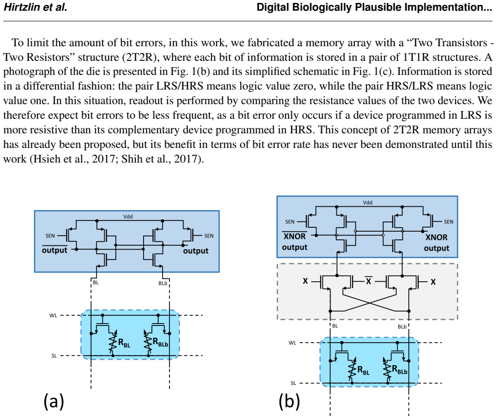
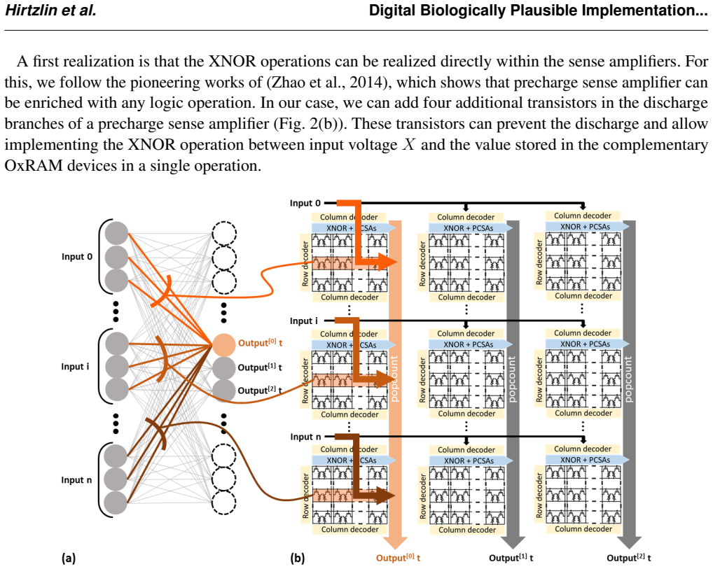
The load-bearing object is the 2T2R differential bit cell paired with a precharge sense amplifier (PCSA). Each bit is stored as a complementary pair of OxRAM devices, one in a low resistance state and one in a high resistance state, so a bit error occurs only if the low-resistance device reads more resistive than its high-resistance partner. The PCSA compares the two resistances through a precharge and discharge cycle, and four additional transistors in its discharge branches gate the discharge on the neuron input voltage; the sense operation itself therefore computes the XNOR of the stored weight and the input. This feeds a digital POPCOUNT circuit, which counts the ones in the XNOR results, and a threshold subtraction, implementing the binarized neuron equation $A_j = \mathrm{sign}(\mathrm{POPCOUNT}_i(\mathrm{XNOR}(W_{ji},X_i)) - T_j)$.
What would settle it
Program a fabricated 2T2R array with known weight patterns, drive the XNOR-enriched sense amplifiers with real neuron input voltages, and compare each output against the expected XNOR truth table; any error rate above the level explained by resistance variability would show that the in-memory XNOR operation is not working as simulated.
Extended reading notes
Core claim
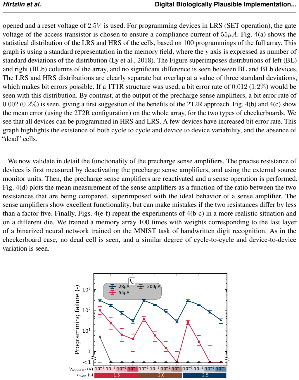
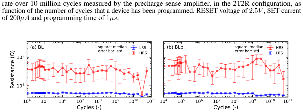
The central discovery is that the differential 2T2R memory structure, combined with the inherent error tolerance of binarized neural networks, makes formal error correction unnecessary for RRAM-based in-memory inference. In a fabricated 1-kilobit array of HfO2 OxRAM devices integrated in the back end of line of a 130 nm CMOS process, 2T2R readout through precharge sense amplifiers holds bit error rates below $10^{-3}$ over 700 million program/erase cycles under strong programming conditions, and below $10^{-4}$ over more than $10^{10}$ cycles under endurance-optimized conditions, while the same devices used as 1T1R cells exceed $10^{-3}$ after a few million cycles. The paper further shows that trained binarized networks keep full accuracy at weight error rates up to $10^{-4}$ and suffer only minimal degradation at $10^{-3}$ across four tasks, and that the read-plus-XNOR-add operation can be integrated into the sense amplifier, estimated at 14 fJ per operation in an advanced node.
Load-bearing premise
The fabricated array was only measured for differential readout of stored weights, not for the XNOR operation with applied neuron inputs; if the added discharge transistors introduce timing asymmetry, voltage-margin loss, or reliability effects, the in-memory computing claim and the 14 fJ per read-plus-add estimate would not transfer from simulation to silicon.
Editorial extensions
If this is right
- RRAM-based inference hardware can drop formal ECC: at weight error rates up to $10^{-3}$, binarized networks show essentially no accuracy loss, removing the area, energy, and latency of syndrome computation.
- Memory devices can be operated in low-energy programming regimes (as low as 20–30 pJ per bit) and high-endurance regimes (beyond $10^{10}$ cycles) while keeping the bit error rate below $10^{-3}$.
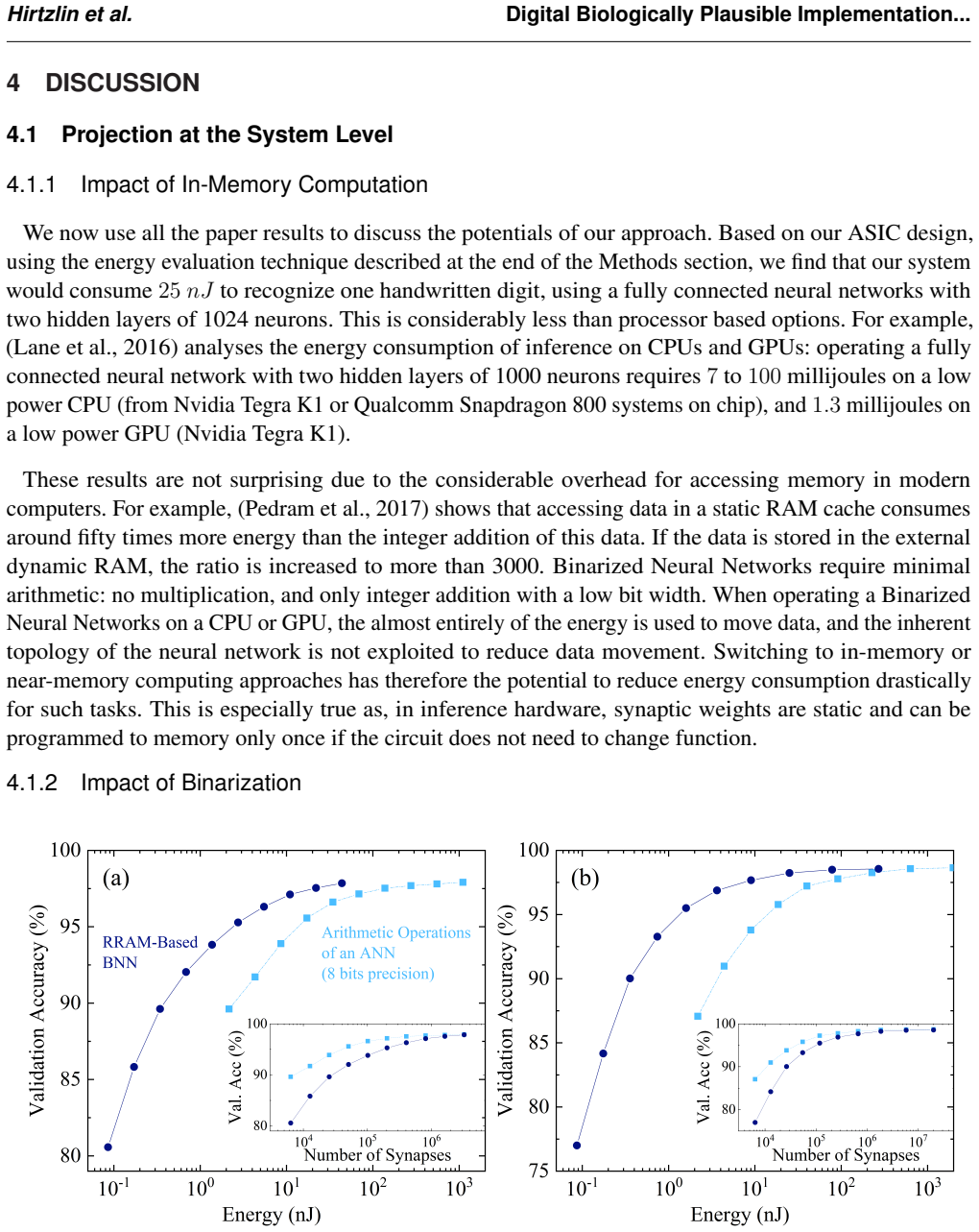
- A full MNIST inference with the proposed system is estimated at 25 nJ, compared with millijoules for CPU and GPU implementations.
- At equal redundancy, the 2T2R differential readout provides bit-error reduction comparable to a SECDED(8,4) Hamming code, but without any decoding logic.
- The energy advantage of binarization over 8-bit fixed-point arithmetic grows as the target accuracy decreases, reaching nearly a factor of ten at lower precision.
Reading between the lines
- If the XNOR-in-sense-amplifier works in silicon, the same differential readout trick could be carried over to other emerging memories such as phase-change or magnetic RAM, since the argument rests on the readout circuit, not on hafnium oxide specifically.
- The measured tolerance to $10^{-3}$ weight errors suggests that write-verify loops, which dominate programming energy in analog RRAM synapses, could be omitted for binary digital weights; a direct energy comparison with and without verify would test this.
- A silicon demonstration of the XNOR-enabled sense amplifier would settle whether the 14 fJ per read-plus-add estimate survives real timing and voltage margins; that figure currently comes from an advanced-node estimate, not from the fabricated 130 nm array.
Signed reviews
Editorial analysis
A structured set of objections, weighed in public.
Referee Report
Summary. This manuscript proposes a digital, biologically inspired implementation of binarized neural network inference using a differential 2T2R HfO2 OxRAM array with precharge sense amplifiers (PCSA) that are designed to perform XNOR operations during readout. The authors fabricated a 1-kb array in a 130 nm CMOS process and characterized its programming, bit-error-rate, and endurance behavior. They report that the 2T2R differential readout reduces synaptic bit error rates by up to four orders of magnitude relative to single-device 1T1R readout in the same programming conditions, and that the benefit is comparable to SEC/SECDED ECC at equivalent redundancy without decoding circuitry. Error-injection simulations on MNIST, CIFAR-10, ImageNet, and ECG tasks show that accuracy is maintained up to weight error rates around 10^-3. A synthesizable SystemVerilog system is described, with energy estimates of 25 nJ per MNIST digit and 14 fJ per read-and-add operation in an advanced node, enabling the use of low-programming-energy (20-30 pJ) and high-endurance (>10^10 cycles) regimes. The paper concludes that the differential architecture allows error-tolerant neural network hardware without formal ECC.
Significance. If fully validated, this would be a valuable demonstration of error-tolerant in-memory computing with emerging nonvolatile memories. The paper's main measured strengths are the direct experimental comparison of 2T2R against 1T1R bit error rates obtained from the same programmed distributions, the extensive endurance measurements over hundreds of millions and tens of billions of cycles, and the error-injection study on four tasks with five repetitions and error bars. These results give a quantitative, falsifiable basis for the claim that differential readout can replace formal ECC in binarized neural network hardware. The significance is partly bounded, however, because the XNOR-in-sense-amplifier operation is presented as a schematic and as part of a system-level simulation, not as a measured circuit function; the silicon data validate only the differential readout. The energy figures are projections, not measured silicon results. With those caveats addressed or the claims reframed, the work would be a solid contribution to the cs.ET / neuromorphic-hardware literature.
major comments (3)
- [Section 2.2, Fig. 2(b); Section 3.1] The manuscript never reports a measurement of the XNOR-augmented PCSA. All silicon data in Section 3.1 (Figs. 4-8) are obtained with the standard differential readout; no experiment applies a neuron input X during sensing and compares the sense-amplifier output against the XNOR truth table for the four (W,X) combinations. Since the four additional transistors lie in the discharge branches that determine the race, their on-resistance and timing can alter the voltage margin characterized in Fig. 4(d). The abstract's claim that the circuit 'allows performing the exclusive NOR operations ... directly within the sense amplifiers' is therefore supported only by schematic and system-level simulation. Please add a measured XNOR-mode characterization, or at minimum a post-layout simulation with the measured RRAM distributions, and adjust the claims accordingly.
- [Section 4.1.3] The 14 fJ per read-plus-addition estimate is an advanced-node projection, not a silicon result, and it assumes the XNOR-augmented PCSA works as drawn in Fig. 2(b). The text states 'in our estimates,' but the assumptions behind this number (technology node, supply voltage, activity factor, inclusion of the XNOR discharge transistors, and whether the RRAM distributions are modeled) are not fully specified. As a projection the figure is acceptable, but it should be clearly labeled as a design estimate for a future implementation rather than as a validated property of the fabricated array.
- [Section 3.2, Fig. 9] The error-tolerance simulations inject bit errors independently and uniformly with probability p, but Section 3.1 shows that hardware errors are not independent: Figs. 4(b)-4(c) and Fig. 5 report device-to-device and cycle-to-cycle variability, and Figs. 6-7 show aging trends. To support the 'without ECC' claim, the tolerance evaluation should also be performed with correlated error maps derived from the measured array (for example, using the per-device error rates of Figs. 4(e-f)) rather than only i.i.d. flips. This would directly test whether the system remains robust to the actual error structure of the fabricated memory.
minor comments (5)
- [Section 2.2] The sentence containing 'while perforning the XNOR operation' contains a typo: 'perforning' should be 'performing'.
- [Introduction, last paragraph] The word 'benckmarking' should be 'benchmarking'.
- [Fig. 5 caption] The caption says 'Number of errors' while the y-axis label appears to be 'Error rate (%)'; please unify these terms and state whether the plotted quantity is a count or a rate.
- [Table 1] The programming-energy ranges are reported without a methodological footnote; please state whether these values are measured from current/voltage waveforms, calculated from programming conditions, or obtained from the system-level simulator.
- [Section 4.1.1] The 25 nJ per digit figure should be explicitly tied to the synthesized system at the considered process node and to the fully connected MNIST network used; currently the sentence reads as a more general statement than the supporting method provides.
Circularity Check
No significant circularity: the 2T2R BER reduction is a direct measurement, BNN error tolerance comes from independent error injection, and the energy projection is from synthesis, not from the target results.
full rationale
The paper's derivation chain is not circular. The 2T2R BER reduction (Figs. 4-8, Section 3.1) is a direct experimental measurement of the fabricated array: the 1T1R BER is obtained from the same programmed resistance distributions via an ideal-threshold calculation, while the 2T2R BER is read by the on-chip precharge sense amplifier, so the comparison is an empirical benchmark rather than a fit. The BNN error-tolerance curves (Section 3.2, Fig. 9) are produced by randomly flipping trained network weights, independently of the measured device BER; they are not fitted to the array data. The system energy estimates (Section 4.1) come from a standard synthesizable SystemVerilog flow with VCD-based power evaluation, and the 14 fJ figure is explicitly stated as an estimate in an advanced node, not a back-fit. The XNOR-in-PCSA building block is imported from prior published work, including co-authored work ('we follow the pioneering works of (Zhao et al., 2014), which shows that precharge sense amplifier can be enriched with any logic operation'), but that prior work is an external circuit-design result and the paper's measured claims do not reduce to it; the absence of a direct measurement of the XNOR operation is a validation gap, not a circular definition. No fitted parameter is renamed as a prediction, and no result is equivalent to its own input by construction.
Assumptions & free parameters
assumptions (4)
- domain assumption Random independent bit flips in all weights represent OxRAM programming and read errors.
- domain assumption The XNOR-enriched PCSA behaves as the schematic in Fig. 2(b) without parasitic imbalance or reliability issues.
- domain assumption Cadence synthesis with VCD activity files gives representative energy for the full system.
- domain assumption Programming conditions in Table 1 satisfy BER below 10^-3 for all tasks because the networks tolerate that rate.
Cite this review
Pith. "Pith review of Digital Biologically Plausible Implementation of Binarized Neural Networks with Differential Hafnium Oxide Resistive Memory Arrays." pith.science (2026). https://pith.science/paper/JTLGGILK
@misc{pith2026190804066,
  author       = {Pith},
  title        = {Pith review of: Digital Biologically Plausible Implementation of Binarized Neural Networks with Differential Hafnium Oxide Resistive Memory Arrays},
  year         = {2026},
  howpublished = {\url{https://pith.science/paper/JTLGGILK}},
  note         = {Machine review of arXiv:1908.04066}
}
read the original abstract
The brain performs intelligent tasks with extremely low energy consumption. This work takes inspiration from two strategies used by the brain to achieve this energy efficiency: the absence of separation between computing and memory functions, and the reliance on low precision computation. The emergence of resistive memory technologies indeed provides an opportunity to co-integrate tightly logic and memory in hardware. In parallel, the recently proposed concept of Binarized Neural Network, where multiplications are replaced by exclusive NOR (XNOR) logic gates, offers a way to implement artificial intelligence using very low precision computation. In this work, we therefore propose a strategy to implement low energy Binarized Neural Networks, which employs brain-inspired concepts, while retaining energy benefits from digital electronics. We design, fabricate and test a memory array, including periphery and sensing circuits, optimized for this in-memory computing scheme. Our circuit employs hafnium oxide resistive memory integrated in the back end of line of a 130 nanometer CMOS process, in a two transistors - two resistors cell, which allows performing the exclusive NOR operations of the neural network directly within the sense amplifiers. We show, based on extensive electrical measurements, that our design allows reducing the amount of bit errors on the synaptic weights, without the use of formal error correcting codes. We design a whole system using this memory array. We show on standard machine learning tasks (MNIST, CIFAR-10, ImageNet and an ECG task) that the system has an inherent resilience to bit errors. We evidence that its energy consumption is attractive compared to more standard approaches, and that it can use the memory devices in regimes where they exhibit particularly low programming energy and high endurance.
Figures

Figures from the paper (7 more)




Reference graph
Works this paper leans on
-
[1]
M., Boybat, I., Nolfo, C., et al
Ambrogio, S., Narayanan, P., Tsai, H., Shelby, R. M., Boybat, I., Nolfo, C., et al. (2018). Equivalent-accuracy accelerated neural-network training using analogue memory. Nature 558, 60 ambrogio2018equivalent
work page 2018
-
[2]
Ando, K., Ueyoshi, K., Orimo, K., Yonekawa, H., Sato, S., Nakahara, H., et al. (2017). Brein memory: A 13-layer 4.2 k neuron/0.8 m synapse binary/ternary reconfigurable in-memory deep neural network accelerator in 65 nm cmos. In Proc. VLSI Symp. on Circuits (IEEE), C24--C25 ando2017brein
work page 2017
-
[3]
Bankman, D., Yang, L., Moons, B., Verhelst, M., and Murmann, B. (2018). An always-on 3.8muj/86 \ with all memory on chip in 28-nm cmos. IEEE Journal of Solid-State Circuits 54, 158--172 bankman2018always
work page 2018
-
[4]
Bocquet, M., Hirztlin, T., Klein, J.-O., Nowak, E., Vianello, E., Portal, J.-M., et al. (2018). In-memory and error-immune differential rram implementation of binarized deep neural networks. In IEDM Tech. Dig. (IEEE), 20.6.1 bocquet2018
work page 2018
-
[5]
Chen, A. (2016). A review of emerging non-volatile memory (nvm) technologies and applications. Solid-State Electronics 125, 25--38 chen2016review
work page 2016
-
[6]
Chen, W. H., Li, K. X., Lin, W. Y., Hsu, K. H., Li, P. Y., Yang, C. H., et al. (2018). A 65nm 1mb nonvolatile computing-in-memory ReRAM macro with sub-16ns multiply-and-accumulate for binary DNN AI edge processors. In Proc. ISSCC . 494--496. doi:10.1109/ISSCC.2018.8310400 chen_65nm_2018
arXiv 2018
-
[7]
Chen, W. H., Lin, W. J., Lai, L. Y., Li, S., Hsu, C. H., Lin, H. T., et al. (2017). A 16mb dual-mode ReRAM macro with sub-14ns computing-in-memory and memory functions enabled by self-write termination scheme. In IEDM Tech . Dig . 28.2.1--28.2.4. doi:10.1109/IEDM.2017.8268468 chen_16mb_2017
-
[8]
Courbariaux, M., Hubara, I., Soudry, D., El-Yaniv, R., and Bengio, Y. (2016). Binarized neural networks: Training deep neural networks with weights and activations constrained to+ 1 or-1. arXiv preprint arXiv:1602.02830 courbariaux2016binarized
arXiv 2016
Show all 53 references
-
[9]
Covi, E., Brivio, S., Serb, A., Prodromakis, T., Fanciulli, M., and Spiga, S. (2016). Analog memristive synapse in spiking networks implementing unsupervised learning. Frontiers in neuroscience 10, 482 covi2016analog
2016
-
[10]
Dong, Q., Kim, Y., Lee, I., Choi, M., Li, Z., Wang, J., et al. (2017). 11.2 a 1mb embedded nor flash memory with 39 w program power for mm-scale high-temperature sensor nodes. In 2017 IEEE International Solid-State Circuits Conference (ISSCC) (IEEE), 198--199 dong201711
2017
-
[11]
Big data needs a hardware revolution
Editorial (2018). Big data needs a hardware revolution. Nature 554, 145. doi:10.1038/d41586-018-01683-1 editorial_big_2018
2018 doi
-
[12]
A., Selen, L
Faisal, A. A., Selen, L. P., and Wolpert, D. M. (2008). Noise in the nervous system. Nature reviews neuroscience 9, 292 faisal2008noise
2008
-
[13]
Giacomin, E., Greenberg-Toledo, T., Kvatinsky, S., and Gaillardon, P.-E. (2019). A robust digital rram-based convolutional block for low-power image processing and learning applications. IEEE Transactions on Circuits and Systems I: Regular Papers 66, 643--654 giacomin2019robust
2019
-
[14]
Gregori, S., Cabrini, A., Khouri, O., and Torelli, G. (2003). On-chip error correcting techniques for new-generation flash memories. Proc. IEEE 91, 602--616 gregori2003chip
2003
-
[15]
Grossi, A., Nowak, E., Zambelli, C., Pellissier, C., Bernasconi, S., Cibrario, G., et al. (2016). Fundamental variability limits of filament-based rram. In IEDM Tech. Dig. (IEEE), 4--7 grossi2016fundamental
2016
-
[16]
Grossi, A., Vianello, E., Zambelli, C., Royer, P., Noel, J.-P., Giraud, B., et al. (2018). Experimental investigation of 4-kb rram arrays programming conditions suitable for tcam. IEEE Transactions on Very Large Scale Integration (VLSI) Systems 26, 2599--2607 grossi2018experimental
2018
-
[17]
Hsieh, W.-T., Chih, Y.-D., Chang, J., Lin, C.-J., and King, Y.-C. (2017). Differential Contact RRAM Pair for Advanced CMOS Logic NVM applications. Proc. SSDM , 171 hsieh_differential_2017
2017
-
[18]
and Wong, H.-S
Ielmini, D. and Wong, H.-S. P. (2018). In-memory computing with resistive switching devices. Nature Electronics 1, 333 ielmini2018memory
2018
-
[19]
and Liu, S.-C
Indiveri, G. and Liu, S.-C. (2015). Memory and information processing in neuromorphic systems. Proc. IEEE 103, 1379--1397 indiveri2015memory
2015
-
[20]
and Szegedy, C
Ioffe, S. and Szegedy, C. (2015). Batch normalization: Accelerating deep network training by reducing internal covariate shift. arXiv preprint arXiv:1502.03167 ioffe2015batch
2015 arXiv
-
[21]
P., Young, C., Patil, N., Patterson, D., Agrawal, G., Bajwa, R., et al
Jouppi, N. P., Young, C., Patil, N., Patterson, D., Agrawal, G., Bajwa, R., et al. (2017). In-datacenter performance analysis of a tensor processing unit. In Proc. ISCA (IEEE), 1--12 jouppi2017datacenter
2017
-
[22]
Kingma, D. P. and Ba, J. (2014). Adam: A method for stochastic optimization. arXiv preprint arXiv:1412.6980 kingma2014adam
2014 arXiv
-
[23]
and Bornholdt, S
Klemm, K. and Bornholdt, S. (2005). Topology of biological networks and reliability of information processing. Proceedings of the National Academy of Sciences 102, 18414--18419 klemm2005topology
2005
-
[24]
and Hinton, G
Krizhevsky, A. and Hinton, G. (2009). Learning multiple layers of features from tiny images. Tech. rep., Citeseer krizhevsky2009learning
2009
-
[25]
Krizhevsky, A., Sutskever, I., and Hinton, G. E. (2012). Imagenet classification with deep convolutional neural networks. In Advances in neural information processing systems. 1097--1105 krizhevsky2012imagenet
2012
-
[26]
D., Bhattacharya, S., Georgiev, P., Forlivesi, C., Jiao, L., Qendro, L., et al
Lane, N. D., Bhattacharya, S., Georgiev, P., Forlivesi, C., Jiao, L., Qendro, L., et al. (2016). Deepx: A software accelerator for low-power deep learning inference on mobile devices. In Proceedings of the 15th International Conference on Information Processing in Sensor Netwo...
2016
-
[27]
LeCun, Y., Bottou, L., Bengio, Y., and Haffner, P. (1998). Gradient-based learning applied to document recognition. Proc. IEEE 86, 2278--2324 lecun1998gradient
1998
-
[28]
Li, C., Belkin, D., Li, Y., Yan, P., Hu, M., Ge, N., et al. (2018). Efficient and self-adaptive in-situ learning in multilayer memristor neural networks. Nature communications 9, 2385 li2018efficient
2018
-
[29]
Lin, X., Zhao, C., and Pan, W. (2017). Towards accurate binary convolutional neural network. In Advances in Neural Information Processing Systems. 345--353 lin2017towards
2017
-
[30]
Ly, D. R. B., Grossi, A., Fenouillet-Beranger, C., Nowak, E., Querlioz, D., and Vianello, E. (2018). Role of synaptic variability in resistive memory-based spiking neural networks with unsupervised learning. J. Phys. D: Applied Physics ly2018role
2018
-
[31]
K., and Strukov, D
Merrikh-Bayat, F., Guo, X., Klachko, M., Prezioso, M., Likharev, K. K., and Strukov, D. B. (2017). High-performance mixed-signal neurocomputing with nanoscale floating-gate memory cell arrays. IEEE transactions on neural networks and learning systems 29, 4782--4790 merrikh2017high
2017
-
[32]
Natsui, M., Chiba, T., and Hanyu, T. (2018). Design of mtj-based nonvolatile logic gates for quantized neural networks. Microelectronics journal 82, 13--21 natsui2018design
2018
-
[33]
Pedram, A., Richardson, S., Horowitz, M., Galal, S., and Kvatinsky, S. (2017). Dark memory and accelerator-rich system optimization in the dark silicon era. IEEE Design & Test 34, 39--50 pedram2017dark
2017
-
[34]
C., Likharev, K
Prezioso, M., Merrikh-Bayat, F., Hoskins, B., Adam, G. C., Likharev, K. K., and Strukov, D. B. (2015). Training and operation of an integrated neuromorphic network based on metal-oxide memristors. Nature 521, 61 prezioso2015training
2015
-
[35]
F., and Gamrat, C
Querlioz, D., Bichler, O., Vincent, A. F., and Gamrat, C. (2015). Bioinspired programming of memory devices for implementing an inference engine. Proc. IEEE 103, 1398--1416 querlioz2015bioinspired
2015
-
[36]
Rastegari, M., Ordonez, V., Redmon, J., and Farhadi, A. (2016). Xnor-net: Imagenet classification using binary convolutional neural networks. In Proc. ECCV (Springer), 525--542 rastegari2016xnor
2016
-
[37]
G., Serrano-Gotarredona, T., Schmidt, H., Lecerf, G., Tomas, J., et al
Sa \" ghi, S., Mayr, C. G., Serrano-Gotarredona, T., Schmidt, H., Lecerf, G., Tomas, J., et al. (2015). Plasticity in memristive devices for spiking neural networks. Frontiers in neuroscience 9, 51 saighi2015plasticity
2015
-
[38]
Serb, A., Bill, J., Khiat, A., Berdan, R., Legenstein, R., and Prodromakis, T. (2016). Unsupervised learning in probabilistic neural networks with multi-state metal-oxide memristive synapses. Nature communications 7, 12611 serb2016unsupervised
2016
-
[39]
P., Hu, M., et al
Shafiee, A., Nag, A., Muralimanohar, N., Balasubramonian, R., Strachan, J. P., Hu, M., et al. (2016). Isaac: A convolutional neural network accelerator with in-situ analog arithmetic in crossbars. ACM SIGARCH Computer Architecture News 44, 14--26 shafiee2016isaac
2016
-
[40]
J., and King, Y.-C
Shih, Y.-H., Hsu, M.-Y., Lin, C. J., and King, Y.-C. (2017). Twin-bit Via RRAM in 16nm FinFET Logic Technologies . Proc. SSDM , 137 shih_twin-bit_2017
2017
-
[41]
(2018 a )
Sun, X., Peng, X., Chen, P.-Y., Liu, R., Seo, J.-s., and Yu, S. (2018 a ). Fully parallel rram synaptic array for implementing binary neural network with (+ 1,- 1) weights and (+ 1, 0) neurons. In Proc. ASP-DAC (IEEE Press), 574--579 sun2018fully
2018
-
[42]
(2018 b )
Sun, X., Yin, S., Peng, X., Liu, R., Seo, J.-s., and Yu, S. (2018 b ). Xnor-rram: A scalable and parallel resistive synaptic architecture for binary neural networks. algorithms 2, 3 sun2018xnor
2018
-
[43]
Tang, T., Xia, L., Li, B., Wang, Y., and Yang, H. (2017). Binary convolutional neural network on rram. In Proc. ASP-DAC (IEEE), 782--787 tang2017binary
2017
-
[44]
Wang, Z., Ambrogio, S., Balatti, S., and Ielmini, D. (2015). A 2-transistor/1-resistor artificial synapse capable of communication and stochastic learning in neuromorphic systems. Frontiers in neuroscience 8, 438 wang20152
2015
-
[45]
Wang, Z., Joshi, S., Savel’ev, S., Song, W., Midya, R., Li, Y., et al. (2018). Fully memristive neural networks for pattern classification with unsupervised learning. Nature Electronics 1, 137 wang2018fully
2018
-
[46]
Yu, S. (2018). Neuro-inspired computing with emerging nonvolatile memorys. Proc. IEEE 106, 260--285 yu2018neuro
2018
-
[47]
Yu, S., Li, Z., Chen, P.-Y., Wu, H., Gao, B., Wang, D., et al. (2016). Binary neural network with 16 mb rram macro chip for classification and online training. In IEDM Tech. Dig. (IEEE), 16--2 yu2016binary
2016
-
[48]
Zhao, W., Chappert, C., Javerliac, V., and Noziere, J.-P. (2009). High speed, high stability and low power sensing amplifier for mtj/cmos hybrid logic circuits. IEEE Transactions on Magnetics 45, 3784--3787 zhao2009high
2009
-
[49]
Zhao, W., Moreau, M., Deng, E., Zhang, Y., Portal, J.-M., Klein, J.-O., et al. (2014). Synchronous non-volatile logic gate design based on resistive switching memories. IEEE Transactions on Circuits and Systems I: Regular Papers 61, 443--454 zhao2014synchronous
2014
-
[50]
, " * write output.state after.block = add.period write newline
ENTRY address author booktitle chapter doi edition editor eid howpublished institution journal key language month note number organization pages publisher school series title type volume year label extra.label sort.label short.list INTEGERS output.state before.all mid.sentence...
-
[51]
write newline
" write newline "" before.all 'output.state := FUNCTION n.dashify 't := "" t empty not t #1 #1 substring "-" = t #1 #2 substring "--" = not "--" * t #2 global.max substring 't := t #1 #1 substring "-" = "-" * t #2 global.max substring 't := while if t #1 #1 substring * t #2 gl...
-
[52]
, " * write output.state after.block = add.period write newline
ENTRY address annote author booktitle chapter doi edition editor eid howpublished institution journal key language month note number organization pages publisher school series title type volume year label extra.label sort.label short.list INTEGERS output.state before.all mid.s...
-
[53]
write newline
" write newline "" before.all 'output.state := FUNCTION n.dashify 't := "" t empty not t #1 #1 substring "-" = t #1 #2 substring "--" = not "--" * t #2 global.max substring 't := t #1 #1 substring "-" = "-" * t #2 global.max substring 't := while if t #1 #1 substring * t #2 gl...
Reviewed August 14, 2026 · model on record in the stance chip above.
Discussion (0). Continue with ORCID to comment.