REVIEW 3 major objections 5 minor 47 references
Stability, efficiency, and mechanism of n-type doping by hydrogen adatoms in two-dimensional transition metal dichalcogenides
T0 review · 3 major / 5 minor · reviewed 2026-08-14 · deepseek-v4-flash
Pith's one-line read Interstitial hydrogen atoms dope TMDC monolayers with one electron each and create no in-gap states.
desk verdict Genuinely new DFT result with a plausible one-electron-per-H doping mechanism; the claim rests on PBE level ordering that deserves a hybrid-functional check before the strongest version is trusted. read the letter →
The pith
A machine-rendered reading of the paper's core claim, the machinery that carries it, and where it could break.
The reading
What carries the argument
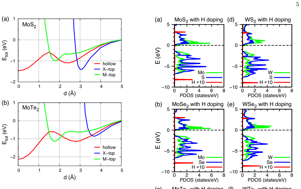
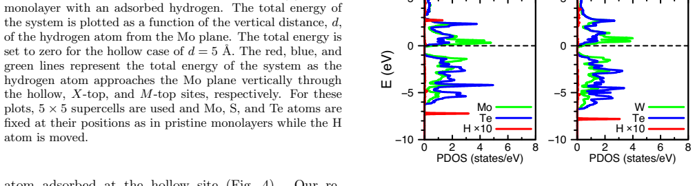
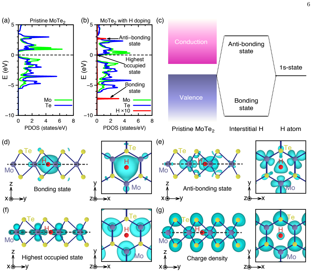
The load-bearing object is the hexagonal hollow site on the transition-metal plane, where interstitial H binds to three metal atoms. Its H 1s orbital hybridizes with metal 5s and 4d orbitals to produce a filled bonding state roughly 7–8 eV below the valence-band maximum and an empty antibonding state roughly 3 eV above the conduction-band minimum; because the antibonding state sits above the conduction-band minimum, the third electron (two from host valence states plus one from H) falls into the conduction band instead. Diffusion barriers are estimated from the binding-energy difference between the hollow site and the saddle-point sites (M-top or X-top), which is a lower bound on the maximum barrier along the path.
What would settle it
A hybrid-functional or many-body GW calculation of H at the hollow site in a selenide or telluride monolayer that places the H-metal antibonding state below the conduction-band minimum, or any state inside the band gap, would overturn the one-electron-per-H donor picture. In experiment, Hall measurements on H-doped monolayer MoTe$_2$ showing an electron density far below the hydrogen concentration, or a thermally activated carrier density, would contradict the claim.
Extended reading notes
Core claim
Hydrogen atoms adsorbed into 1H-phase monolayer TMDCs ($MX_2$ with $M = \mathrm{Mo}, \mathrm{W}$ and $X = \mathrm{S}, \mathrm{Se}, \mathrm{Te}$) are most stable at the center of the hexagonal hollow site lying directly on the transition-metal plane, where each H atom donates exactly one electron to the conduction bands and creates no defect state inside the band gap. The diffusion barrier for leaving that site grows from sulfides to selenides to tellurides, reaching 0.67–0.93 eV in the selenides and tellurides, so the dopants are effectively immobile at room temperature. The doping mechanism is the formation of a bonding state far below the valence-band maximum and an antibonding state about 3 eV above the conduction-band minimum from the H 1s orbital and metal orbitals; the antibonding state remains empty because it lies above the conduction band, and the electron that would occupy it instead goes into the conduction band. For comparison, H$_2$ molecules dope p-type, and H atoms at Te vacancies compensate the p-doping of the vacancy.
Load-bearing premise
The load-bearing premise is that the generalized-gradient-approximation functional places the hydrogen-metal bonding state about 7–8 eV below the valence-band maximum and the antibonding state about 3 eV above the conduction-band minimum, so its well-known band-gap underestimation cannot shift either state into the gap or bring the donor level below the conduction-band minimum.
Editorial extensions
If this is right
- Hydrogen atoms can locally convert p-type MoTe$_2$ to n-type, allowing p-n junctions or more complex circuits within a single TMDC nanosheet.
- In selenide and telluride monolayers, barriers of 0.67–0.93 eV mean patterned hydrogen doping will not blur by diffusion at room temperature.
- Because no defect state lies in the gap and the donor state is above the conduction-band minimum, conduction electrons see little added scattering and the carrier density equals the hydrogen density, independent of temperature.
- Hydrogen molecules, which form when two H atoms meet, dope p-type instead, so preserving the n-type effect requires keeping hydrogen atoms isolated from one another.
- Hydrogen atoms at tellurium vacancies neutralize the vacancy's hole doping, enabling net p-to-n conversion in realistic samples that contain such vacancies.
Reading between the lines
- The same orbital-counting argument implies a ceiling on useful hydrogen dose: once neighboring H atoms pair into H$_2$, the doping switches from n-type to p-type, so the maximum n-type carrier density is set by the H-pairing distance rather than by the adsorption site.
- Because the global minimum is reached only after passing a shallow local minimum a few ångströms off the metal plane, low-temperature deposition may leave hydrogen at the wrong site; an annealing step or elevated substrate temperature should be needed to realize the one-electron doping in practice.
- The donor mechanism should transfer to other two-dimensional semiconductors whose conduction band has strong metal-d character: an interstitial s-orbital impurity will dope efficiently when its antibonding partner lies above the conduction-band minimum. Testing hydrogen in other $MX_2$ compounds would map the scope of this design rule.
Signed reviews
Editorial analysis
A structured set of objections, weighed in public.
Referee Report
Summary. This paper reports first-principles DFT-PBE-D2 calculations of hydrogen in 1H-phase monolayer (and some bulk and bilayer) Mo/W dichalcogenides. It claims that H is most stable at the interstitial hollow site on the transition-metal plane, that diffusion barriers increase from sulfides to selenides to tellurides, and that each interstitial H donates exactly one electron to the conduction band while producing no in-gap defect state. The proposed mechanism is formation of bonding and antibonding states between the H 1s state and nearby metal s/d orbitals, with the antibonding state lying about 3 eV above the CBM, so that one electron transfers to the CBM. The paper also compares H2 adsorption and Te-vacancy-related defects, concluding that interstitial hydrogen is a promising stable n-type dopant for patterned TMDC devices.
Significance. If the one-electron-per-H doping and absence of in-gap states are correct, the result is a design-relevant and falsifiable prediction for n-type doping of TMDCs, with practical implications for ALD-based patterned doping. The paper has several genuine strengths: it carefully counts states and electrons; it estimates BSSE; it cross-checks the site preference with VASP for MoS2 and MoTe2; it uses large 5x5 supercells with a 100-angstrom vacuum; and it provides wavefunction and charge-density analysis of the doping mechanism. The main risks are the functional dependence of the donor-level position and the lack of true diffusion saddle-point calculations.
major comments (3)
- [Section III.B, Fig. 5(b)] The central one-electron-per-H conclusion rests on the PBE-D2 result that the H antibonding state lies about 3 eV above the PBE CBM. The paper argues that the well-known band-gap underestimation cannot affect this conclusion, but that argument is incomplete: Kohn-Sham eigenvalue errors from self-interaction and delocalization can shift a localized resonance relative to the host band edges by an amount that is not controlled by the gap error alone. A hybrid-functional (HSE) or G0W0 calculation for at least one representative compound, such as MoTe2 or MoS2, is needed to verify that the antibonding state remains above the true CBM and that no occupied defect state enters the gap. As written, the headline doping mechanism is supported by a single exchange-correlation approximation.
- [Section III.A, Table I] The quantity called the diffusion barrier, E_barr, is defined as the binding-energy difference between the hollow site and the M-top or X-top site; it is not a saddle-point barrier. Without nudged-elastic-band or equivalent minimum-energy-path calculations, the values 0.14-0.93 eV are only lower bounds, and for MoS2 and WS2 the reported lower bounds (0.143 and 0.353 eV) are below the room-temperature scale. The claim of substantial barriers and negligible diffusion should be supported by actual barrier calculations for at least the sulfides and one telluride.
- [Section II, Table I] The 5x5-supercell binding energies are obtained by transplanting atomic coordinates relaxed in a 3x3 supercell without a stated re-relaxation in the 5x5 cell. At hydrogen concentrations of 1/9 versus 1/25, the optimal local relaxation around H is not guaranteed to be the same, and the residual strain can bias binding-energy differences by amounts comparable to the reported MoS2 barrier. The authors should either fully relax the 5x5 supercell or demonstrate that the transplanted geometry and a fully relaxed one give the same energies.
minor comments (5)
- [Abstract and Introduction] The text uses 'adsorbed hydrogen atoms' for the lowest-energy configuration, but that configuration is an interstitial site on the transition-metal plane; consider using 'interstitial hydrogen' to avoid confusion with surface adatoms.
- [Table IV and Fig. 8] The notation 'h doping' should be replaced by 'hole doping' or 'p-type doping' for consistency with the rest of the text.
- [Section III.A] The term 'diffusion barrier height' for E_barr should be replaced by 'site-energy difference' or an explicit lower-bound qualifier until true minimum-energy-path barriers are computed.
- [Footnote 45] The VASP cross-check is useful but should be expanded in the main text with the functional, supercell size, and the computed site-energy differences so that its scope is clear.
- [Section II] The manuscript does not state explicitly whether spin polarization was allowed in the DFT calculations; since a neutral H impurity introduces an unpaired electron if localized, this choice should be stated and checked.
Circularity Check
No significant circularity: the one-electron-per-H doping claim is obtained from DFT state counting and wavefunction analysis, not from a fitted parameter or self-citation chain.
full rationale
The central claims are computed from first-principles DFT: binding energies, diffusion barriers, projected density of states, and wavefunctions. The 'one electron per hydrogen atom' result is extracted in Section III.B and Figs. 4 and 5 by counting occupied states below the VBM before and after H adsorption and by locating the H-induced bonding and antibonding resonances well outside the band gap. This is a derived output, not an input assumption: no parameter is fitted to reproduce the doping rate, and the conclusion would fail if the calculated level ordering placed an antibonding state inside the gap. The self-citations (Refs. 41 and 42 for methodology, Ref. 28 for hydrogen release in ALD) are background and do not carry the derivation. The VASP cross-check in footnote 45 independently reproduces the site preference. The reliance on PBE without hybrid or GW validation is a correctness and robustness concern about the level ordering, not a circularity: the paper explicitly argues that the large separations of the defect states from the band edges make the conclusion insensitive to band-gap underestimation. Whether that error-magnitude argument is quantitatively sufficient is an open scientific question, but it does not reduce the prediction to its inputs.
Assumptions & free parameters
assumptions (3)
- domain assumption PBE-GGA with DFT-D2 gives accurate relative adsorption energies and diffusion barriers for hydrogen in TMDC monolayers.
- ad hoc to paper PBE band-gap underestimation is too small, relative to the defect-state distances of 7-8 eV below VBM and about 3 eV above CBM, to create an in-gap defect state or to move the donor level below the conduction band minimum.
- domain assumption One hydrogen in a 5x5 supercell is dilute enough that hydrogen-hydrogen image interactions and finite-size effects do not change the qualitative doping conclusions.
Cite this review
Pith. "Pith review of Stability, efficiency, and mechanism of n-type doping by hydrogen adatoms in two-dimensional transition metal dichalcogenides." pith.science (2026). https://pith.science/paper/DIIZ7MV3
@misc{pith2026190804360,
  author       = {Pith},
  title        = {Pith review of: Stability, efficiency, and mechanism of n-type doping by hydrogen adatoms in two-dimensional transition metal dichalcogenides},
  year         = {2026},
  howpublished = {\url{https://pith.science/paper/DIIZ7MV3}},
  note         = {Machine review of arXiv:1908.04360}
}
read the original abstract
Mono- and few-layer transition-metal dichalcogenides (TMDCs) provide opportunities for ideal two-dimensional semiconductors for electronic and optoelectronic devices. For electronic devices on TMDCs, it is essential to incorporate n- and/or p-type dopants which are stable in positions after patterned doping. Here we investigate hydrogen doping for TMDC (MX2 with M = Mo, W and X = S, Se, Te) nanosheets by first-principles calculations to address diffusion and doping properties. We find that adsorbed hydrogen atoms in TMDCs are energetically most stable at the interstitial site right on the Mo or W plane and have substantial energy barriers against diffusion that increase in the order of sulfides, selenides, and tellurides. Located at the most stable interstitial site on the Mo or W plane, the hydrogen atoms produce electrons in the conduction bands in the extremely high rate of one electron per hydrogen atom, without any defect state inside the band gap remarkably. We analyze the chemical bonding character around the dopant and the mechanism for such high efficiency of electron doping. We also consider properties of hydrogen molecules and Te vacancies for comparison. Our work shows that hydrogen doping is the promising pathway to development of highly integrated electronic devices on TMDCs
Figures


Figures from the paper (4 more)


Reference graph
Works this paper leans on
-
[1]
B. Radisavljevic, A. Radenovic, J. Brivio, V. Giacometti, and A. Kis, Nat. Nanotech. 6, 147 (2011)
work page 2011
-
[2]
H. Wang, L. Yu, Y.-H. Lee, Y. Shi, A. Hsu, M. L. Chin, L.-J. Li, M. Dubey, J. Kong, and T. Palacios, Nano Lett. 12, 4674 (2012)
work page 2012
-
[3]
Q. H. Wang, K. Kalantar-Zadeh, A. Kis, J. N. Coleman, and M. S. Strano, Nat. Nanotech. 7, 699 (2012)
work page 2012
-
[4]
D. H. Keum, S. Cho, J. H. Kim, D.-H. Choe, H.-J. Sung, M. Kan, H. Kang, J.-Y. Hwang, S. W. Kim, H. Yang, K. J. Chang, and Y. H. Lee, Nat. Phys. 11, 482 (2015)
work page 2015
-
[5]
H. S. Lee, S. S. Baik, K. Lee, S.-W. Min, P. J. Jeon, J. S. Kim, K. Choi, H. J. Choi, J. H. Kim, and S. Im, ACS Nano 9, 8312 (2015)
work page 2015
- [6]
-
[7]
H. Fang, M. Tosun, G. Seol, T. C. Chang, K. Takei, J. Guo, and A. Javey, Nano Lett. 13, 1991 (2013)
work page 2013
-
[8]
Y.-C. Lin, D. O. Dumcenco, H.-P. Komsa, Y. Niimi, A. V. Krasheninnikov, Y.-S. Huang, and K. Suenaga, Adv. Mater. 26, 2857 (2014)
work page 2014
Show all 47 references
-
[9]
Suh, T.-E
J. Suh, T.-E. Park, D.-Y. Lin, D. Fu, J. Park, H. J. Jung, Y. Chen, C. Ko, C. Jang, Y. Sun, R. Sinclair, J. Chang, S. Tongay, and J. Wu, Nano Lett. 14, 6976 (2014)
2014
-
[10]
B. Chen, H. Sahin, A. Suslu, L. Ding, M. I. Bertoni, F. M. Peeters, and S. Tongay, ACS Nano 9, 5326 (2015)
2015
-
[11]
Lee, G.-H
C.-H. Lee, G.-H. Lee, A. M. van der Zande, W. Chen, Y. Li, M. Han, X. Cui, G. Arefe, C. Nuckolls, T. F. Heinz, J. Guo, J. Hone, and P. Kim, Nat. Nanotech. 9, 676 (2014)
2014
-
[12]
Pezeshki, S
A. Pezeshki, S. H. H. Shokouh, P. J. Jeon, I. Shackery, J. S. Kim, I.-K. Oh, S. C. Jun, H. Kim, and S. Im, ACS Nano 10, 1118 (2016)
2016
-
[13]
Z. Lin, B. R. Carvalho, E. Kahn, R. Lv, R. Rao, H. Terrones, M. A. Pimenta, and M. Terrones, 2D Mater.3, 022002 (2016)
2016
-
[14]
J. G. He, K. C. Wu, R. J. Sa, Q. H. Li, and Y. Q. Wei, Appl. Phys. Lett. 96, 082504 (2010)
2010
-
[15]
Y. Ma, Y. Dai, M. Guo, C. Niu, J. Lu, and B. Huang, Phys. Chem. Chem. Phys. 13, 15546 (2011). 10
2011
-
[16]
Voiry, R
D. Voiry, R. Fullon, J. Yang, C. C. C. Silva, R. Kappera, I. Bozkurt, D. Kaplan, M. J. Lagos, P. E. Batson, G. Gupta, A. D. Mohite, L. Dong, D. Er, V. B. Shenoy, T. Asefa, and M. Chhowalla, Nat. Mater. 15, 1003 (2016)
2016
-
[17]
Y. Kim, Y. I. Jhon, J. Park, C. Kim, S. Lee, and Y. M. Jhon, Sci. Rep. 6, 21405 (2016)
2016
-
[18]
L. K. Li, Y. J. Yu, G. J. Ye, Q. Q. Ge, X. D. Ou, H. Wu, D. L. Feng, X. H. Chen, and Y. B. Zhang, Nat. Nanotech. 9, 372 (2014)
2014
-
[19]
J. Kim, S. S. Baik, S. H. Ryu, Y. Sohn, S. Park, B.-G. Park, J. Denlinger, Y. Yi, H. J. Choi, and K. S. Kim, Science 349, 723 (2015)
2015
-
[20]
S. S. Baik, K. S. Kim, Y. Yi, and H. J. Choi, Nano Lett. 15, 7788 (2015)
2015
-
[21]
Doh and H
H. Doh and H. J. Choi, 2D Mater. 4, 025071 (2017)
2017
-
[22]
Y. Yan, B. Xia, Z. Xu, and X. Wang, ACS Catal. 4, 1693 (2014)
2014
-
[23]
Qi, Y.-W
J. Qi, Y.-W. Lan, A. Z. Stieg, J.-H. Chen, Y.-L. Zhong, L.-J. Li, C.-D. Chen, Y. Zhang, and K. L. Wang, Nat. Commun. 6, 7430 (2015)
2015
-
[24]
M. M. Aly¨ or¨ uk, Y. Aierken, D. C ¸ akir, F. M. Peeters, and C. Sevik, J. Phys. Chem. C 119, 23231 (2015)
2015
-
[25]
Z. Yin, H. Li, H. Li, L. Jiang, Y. Shi, Y. Sun, G. Lu, Q. Zhang, X. Chen, and H. Zhang, ACS Nano 6, 74 (2012)
2012
-
[26]
Lopez-Sanchez, D
O. Lopez-Sanchez, D. Lembke, M. Kayci, A. Radenovic, and A. Kis, Nat. Nanotech. 8, 497 (2013)
2013
-
[27]
X. Xu, W. Yao, D. Xiao, and T. F. Heinz, Nat. Phys. 10, 343 (2014)
2014
-
[28]
J. Y. Lim, A. Pezeshki, S. Oh, J. S. Kim, Y. T. Lee, S. Yu, D. K. Hwang, G.-H. Lee, H. J. Choi, and S. Im, Adv. Mater 29, 1701798 (2017)
2017
-
[29]
R. C. Newman, Rep. Prog. Phys. 45, 1163 (1982)
1982
-
[30]
C. G. van de Walle and J. Neugebauer, Annu. Rev. Mater. Res. 36, 179 (2006)
2006
-
[31]
U. M. Gosele, Annu. Rev. Mater. Sci. 18, 257 (1988)
1988
-
[32]
S. J. Pearton, J. W. Corbett, and T. S. Shi, Appl. Phys. A 43, 153 (1987)
1987
-
[33]
C. G. Van de Walle, Phys. Rev. Lett. 85, 1012 (2000)
2000
-
[34]
K. J. Chang and D. J. Chadi, Phys. Rev. B 40, 11644 (1989)
1989
-
[35]
J. P. Perdew, K. Burke, and M. Ernzerhof, Phys. Rev. Lett. 77, 3865 (1996)
1996
-
[36]
Troullier and J
N. Troullier and J. L. Martins, Phys. Rev. B 43, 1993 (1991)
1991
-
[37]
J. M. Soler, E. Artacho, J. D. Gale, A. Garcia, J. Jun- quera, P. Ordej´ on, and D. S´ anchez-Protal, J. Phys.: Con- dens. Matter 14, 2745 (2002)
2002
-
[38]
Kleinman, Phys
L. Kleinman, Phys. Rev. B 21, 2630 (1980)
1980
-
[39]
Theurich and N
G. Theurich and N. A. Hill, Phys. Rev. B 64, 073106 (2001)
2001
-
[40]
Kleinman and D
L. Kleinman and D. M. Bylander, Phys. Rev. Lett. 48, 1425 (1982)
1982
-
[41]
C.-Y. Moon, J. Han, H. Lee, and H. J. Choi, Phys. Rev. B 84, 195425 (2011)
2011
-
[42]
Oh and H
S. Oh and H. J. Choi, Sci. Rep. 7, 2024 (2017)
2017
-
[43]
Kresse and J
G. Kresse and J. Hafner, Phys. Rev. B 47, 558 (1993)
1993
-
[44]
Kresse and J
G. Kresse and J. Furthm¨ uller, Phys. Rev. B 54, 11169 (1996)
1996
-
[45]
Our VASP results also show the hy- drogen atom adsorbed at the hollow site on the metal plane is the lowest energy configuration, confirming our SIESTA results
By using VASP, we obtained the binding energy of the hydrogen atom adsorbed at various sites in monolayer MoS2 and MoTe2. Our VASP results also show the hy- drogen atom adsorbed at the hollow site on the metal plane is the lowest energy configuration, confirming our SIESTA results
-
[46]
The Fermi-Dirac occupation number of each state is summed for the band indexn and the wave vector k, divided by the number of k points
We used the standard method to count the number of electrons. The Fermi-Dirac occupation number of each state is summed for the band indexn and the wave vector k, divided by the number of k points
-
[47]
Here kB is Boltzmann constant and T is the temperature of the system
When a system has a finite energy difference (∆ E) be- tween highest occupied states ( E1) and lowest unoc- cupied states ( E2), the chemical potential determined by the Fermi-Dirac distribution can deviate by the or- der of kBT from ( E1 + E2)/2. Here kB is Boltzmann constant a...
Reviewed August 14, 2026 · model on record in the stance chip above.
Discussion (0). Continue with ORCID to comment.