REVIEW 3 major objections 5 minor 27 references
Point group symmetry of cadmium arsenide thin films determined by convergent beam electron diffraction
T0 review · 3 major / 5 minor · reviewed 2026-08-14 · deepseek-v4-flash
Pith's one-line read Convergent beam electron diffraction shows that molecular-beam-epitaxy-grown Cd3As2 thin films belong to the centrosymmetric tetragonal point group 4/mmm, making them Dirac semimetals.
desk verdict Careful CBED work that convincingly places MBE-grown Cd3As2 in the centrosymmetric 4/mmm point group, with the caveat that the crucial symmetry call is visual. read the letter →
The pith
A machine-rendered reading of the paper's core claim, the machinery that carries it, and where it could break.
The reading
What carries the argument
The central object is whole-pattern CBED symmetry, specifically the presence of two perpendicular mirror planes in the $[\bar{1}10]$ whole pattern including the higher-order Laue zone rings. Because dynamical electron diffraction breaks the usual centrosymmetric intensity relation, the whole-pattern symmetry directly reports the three-dimensional point group. The paper pairs this with the diffraction-group classification tables and with Bloch wave simulations of both candidate structures; the simulation shows that the non-centrosymmetric I41cd model gives only one mirror in the $[\bar{1}10]$ whole pattern, while the centrosymmetric I41/acd model gives 2mm.
What would settle it
Re-record the $[\bar{1}10]$ whole-pattern CBED under controlled thickness and tilt and compute a quantitative mirror-symmetry score, for example the correlation between the pattern and its reflection across each candidate mirror. If either mirror score is not clearly above the noise level, or if a Bloch wave calculation for I41cd with the same absorption and thickness parameters as the experiment also shows 2mm whole-pattern symmetry, the paper's central claim is falsified.
Extended reading notes
Core claim
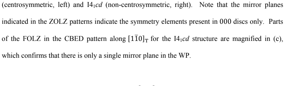
The paper reports that MBE-grown Cd3As2 films are centrosymmetric with point group 4/mmm, the same point group as the bulk I41/acd structure. The decisive evidence is the $[\bar{1}10]$ zone-axis CBED pattern, where both the bright-field disc and the whole pattern show 2mm symmetry. According to the diffraction-group tables, that combination is compatible with 4/mmm and incompatible with the non-centrosymmetric 4mm point group, for which the whole pattern would show only one mirror. Bloch wave simulations for the two reported structures reproduce this difference, and HAADF-STEM images show the systematically ordered Cd vacancies of the I41/acd structure. Along $[001]$, the pattern shows 4mm symmetry; combined with the other zone axes this narrows the point group to 4/mmm rather than m3m.
Load-bearing premise
The conclusion depends on the visual judgment that the experimental $[\bar{1}10]$ whole-pattern CBED has two perpendicular mirrors, and on Bloch wave simulations that reproduce the difference between the two structures; if beam tilt, specimen bending, thickness, or absorption effects changed the apparent symmetry, or if the simulation parameters favored one structure, the 4/mmm assignment would fail.
Editorial extensions
If this is right
- Because the films belong to 4/mmm, electronic-structure predictions based on the centrosymmetric bulk structure apply directly to MBE-grown films.
- The film structure is not altered by residual strain or low growth temperature, so the symmetry-protected Dirac nodes should survive in the thin-film geometry.
- Whole-pattern CBED symmetry, particularly the $[\bar{1}10]$ 2mm pattern, discriminates between I41/acd and I41cd in cases where x-ray diffraction cannot.
- The intermediate-temperature P42/nmc phase is excluded for these films; HAADF-STEM identifies the vacancy arrangement as that of I41/acd.
Reading between the lines
- A quantitative check would be to apply a pixel-level mirror-symmetry statistic to the recorded $[\bar{1}10]$ whole pattern; the paper reports no such metric and relies on visual inspection.
- If the assignment is correct, angle-resolved photoemission and magnetotransport on these films should show one Dirac node pair and no chiral surface Fermi arcs; looking for the absence of Fermi arcs is a testable consequence the paper does not pursue.
- The same diffraction-group strategy could settle inversion-center debates in other vacancy-ordered topological materials where x-ray diffraction is ambiguous.
- A caveat implicit in the paper is that the intermediate-temperature P42/nmc phase also belongs to 4/mmm, so CBED alone cannot distinguish it from I41/acd; the HAADF-STEM vacancy pattern is what breaks that tie.
Signed reviews
Editorial analysis
A structured set of objections, weighed in public.
Referee Report
Summary. The manuscript reports a convergent beam electron diffraction (CBED) study of molecular-beam-epitaxy-grown Cd3As2 thin films. From the symmetries of the bright-field discs and whole patterns recorded along [2-01], [021], [1-10] and [001], together with HAADF-STEM imaging and Bloch wave simulations, the authors conclude that the films belong to the centrosymmetric tetragonal point group 4/mmm (space group I41/acd), and therefore are Dirac semimetals. The key differentiating observation is the claimed 2mm symmetry in the [1-10] whole pattern, which is expected for 4/mmm but not for the noncentrosymmetric 4mm (I41cd) structure.
Significance. If the conclusion is correct, the paper resolves an important structural ambiguity for thin-film Cd3As2: it assigns the centrosymmetric structure, aligning the films with the Dirac-semimetal description and showing that MBE growth and strain relaxation do not alter the bulk vacancy ordering. The multiple-zone-axis strategy, use of the Buxton tables, and comparison with Bloch wave simulations of both candidate structures are appropriate and give the argument a coherent internal logic. The paper's usefulness would be enhanced by making the symmetry evaluation quantitative and by reporting simulation parameters; in its present form the decisive step rests on visual inspection of a small number of patterns.
major comments (3)
- [Results and Discussion, Fig. 3] The central claim that the films have 4/mmm rather than 4mm rests on the assignment of 2mm symmetry to the experimental [1-10] whole pattern (WP), but this assignment is made by eye from a single false-colored pattern and no quantitative symmetry metric is reported. A pattern with one mirror plus noise can easily be read as having two mirrors, and the second mirror is the only feature that distinguishes 4/mmm from 4mm in this zone axis; as the authors themselves note, the bright-field disc along [1-10] cannot discriminate between the two point groups. Please provide a quantitative symmetry measure (for example, intensity residuals after imposing the candidate mirror operations, or a correlation coefficient against symmetrized versions), and show the unprocessed or minimally processed patterns, so that the 2mm-versus-m decision can be checked independently.
- [Results and Discussion, Fig. 4] The Bloch wave simulations are used as confirmation of the Buxton-table analysis, but the manuscript gives no simulation parameters (thickness, absorption parameters, Debye-Waller factors, accelerating voltage, orientation or beam tilt) and no quantitative comparison between simulated and experimental patterns. Without these, the reader cannot assess whether the simulated I41cd [1-10] WP is representative of the experimental scattering conditions or whether the absence of the second mirror in that simulation is robust. Please include the input parameters and a direct side-by-side comparison with the experimental pattern, ideally using the same symmetry metric applied to the data.
- [Results and Discussion, Table I and Fig. 5] The final discrimination between 4/mmm and m3m in Table I relies on the HAADF-STEM evidence for ordered Cd vacancies and on the observed differences in HOLZ ring diameters between zones A, B and C. This reasoning is reasonable, but the paper does not show the supplementary <100> WP that is cited in the text as additional confirmation; please show that pattern or explicitly describe how it enters the point-group intersection. Without it, the argument that the additional zone axis rules out m3m is not fully documented in the main text.
minor comments (5)
- [Abstract and Introduction] The phrase 'reported room temperature crystal structures of Cd3As2 reported differ' is redundant; please rephrase for clarity.
- [Fig. 3 caption] Figure 3(b) is described as a magnification of parts of the FOLZ in the [1-10] WP, but the caption does not state the exact region or the magnification; a dashed box in Fig. 3(a) would help the reader locate the magnified area.
- [References] Reference [26] gives 'A. Pietrasz' and 'K. Lukaszew', but the same authors appear as 'Pietraszko' and 'Lukaszewicz' in Reference [17]; please check and correct these names.
- [Table I] Table I is difficult to read because all possible point groups are concatenated in a single column; a properly formatted table with separate rows for each zone axis and each candidate point group would improve clarity.
- [Results and Discussion] The statement that 'additional confirmation' comes from a <100> WP refers to the Supplemental Material but does not cite a specific supplementary figure; please add the figure number.
Circularity Check
No significant circularity: the point group conclusion is derived from measured CBED symmetries against external Buxton tables and literature-structure simulations.
full rationale
No circular step is present. The paper's central claim that MBE-grown Cd3As2 films belong to the centrosymmetric point group 4/mmm is derived from experimentally observed CBED pattern symmetries (m in [201] and [021] BPs/WPs; 2mm in the [110] BP and WP; 4mm in [001]) compared with the published Buxton et al. diffraction-group tables [19]. The Bloch wave simulations for the I41/acd and I41cd structures are not fitted to the target conclusion: they are parameter-free symmetry calculations for the two published literature structures, and the discriminating difference (2mm vs m in the [110] whole pattern) is a consequence of the known point groups, not a fitted output. The zone-axis indexing is geometric, based on the FOLZ ring radius. Self-citations [22,23] concern film growth and twin suppression, not the symmetry determination; the citation to Zuo's CBED simulation code [21,24] is a methods citation, not load-bearing. The paper is self-contained against external benchmarks: the Buxton tables and the literature structures. A possible concern about the visual assignment of 2mm symmetry in the experimental [110] WP is an experimental reliability issue, not a circularity issue, because the paper does not fit a parameter to that pattern and then re-predict it. Therefore the derivation chain does not reduce to its own inputs.
Assumptions & free parameters
assumptions (3)
- standard math Buxton et al. diffraction group to point group tables are correct and applicable to the observed CBED patterns
- domain assumption Dynamical Bloch wave simulations faithfully reproduce CBED symmetries of the two proposed Cd3As2 structures
- domain assumption The MBE films are relaxed and bulk-like, so the thin film symmetry reflects the intrinsic crystal structure
Cite this review
Pith. "Pith review of Point group symmetry of cadmium arsenide thin films determined by convergent beam electron diffraction." pith.science (2026). https://pith.science/paper/W5JDKKJX
@misc{pith2026190805734,
  author       = {Pith},
  title        = {Pith review of: Point group symmetry of cadmium arsenide thin films determined by convergent beam electron diffraction},
  year         = {2026},
  howpublished = {\url{https://pith.science/paper/W5JDKKJX}},
  note         = {Machine review of arXiv:1908.05734}
}
read the original abstract
Cadmium arsenide (Cd3As2) is one of the first materials to be discovered to belong to the class of three-dimensional topological semimetals. Reported room temperature crystal structures of Cd3As2 reported differ subtly in the way the Cd vacancies are arranged within its antifluorite-derived structure, which determines if an inversion center is present and if Cd3As2 is a Dirac or Weyl semimetal. Here, we apply convergent beam electron diffraction (CBED) to determine the point group of Cd3As2 thin films grown by molecular beam epitaxy. Using CBED patterns from multiple zone axes, high-angle annular dark-field images acquired in scanning transmission electron microscopy, and Bloch wave simulations, we show that Cd3As2 belongs to the tetragonal 4/mmm point group, which is centrosymmetric. The results show that CBED can distinguish very subtle differences in the crystal structure of a topological semimetal, a capability that will be useful for designing materials and thin film heterostructures with topological states that depend on the presence of certain crystal symmetries.
Figures


Figures from the paper (3 more)


Reference graph
Works this paper leans on
-
[1]
T. O. Wehling, A. M. Black-Schaffer, and A. V. Balatsky, Adv. Phys. 63, 1 (2014)
work page 2014
-
[21]
J. C. H. Spence, and J. M. Zuo, Electron Microdiffraction (Plenum Press, New York, 1992)
work page 1992
- [2]
-
[3]
N. P. Armitage, E. J. Mele, and A. Vishwanath, Rev. Mod. Phys. 90, 015001 (2018)
2018
-
[4]
M. Kargarian, M. Randeria, and Y. M. Lu, Proc. Natl. Acad. Sci. 113, 8648 (2016)
work page 2016
-
[5]
Z. J. Wang, H. M. Weng, Q. S. Wu, X. Dai, and Z. Fang, Phys. Rev. B 88, 125427 (2013)
work page 2013
-
[6]
M. Neupane, S. Y. Xu, R. Sankar, N. Ali doust, G. Bian, C. Liu, I. Belopolski, T. R. Chang, H. T. Jeng, H. Lin, A. Bansil, F. Chou, and M. Z. Hasan, Nat. Comm. 5, 3786 (2014)
work page 2014
-
[7]
S. Jeon, B. B. Zhou, A. Gyenis, B. E. Feldma n, I. Kimchi, A. C. Potter, Q. D. Gibson, R. J. Cava, A. Vishwanath, and A. Yazdani, Nat. Mater. 13, 851 (2014)
work page 2014
Show all 27 references
-
[8]
Liang, Q
T. Liang, Q. Gibson, M. N. Ali, M. H. Li u, R. J. Cava, and N. P. Ong, Nat. Mater. 14, 280 (2015)
2015
-
[9]
Borisenko, Q
S. Borisenko, Q. Gibson, D. Evtushinsky, V. Zabolotnyy, B. Buchner, and R. J. Cava, Phys. Rev. Lett. 113, 165109 (2014)
2014
-
[10]
Z. K. Liu, J. Jiang, B. Zhou, Z. J. Wa ng, Y. Zhang, H. M. Weng, D. Prabhakaran, S.-K. Mo, H. Peng, P. Dudin, T. Kim, M. Hoesch, Z. Fang, X. Dai, Z. X. Shen, D. L. Feng, Z. Hussain, and Y. L. Chen, Nat. Mater. 13, 677 (2014)
2014
-
[11]
Crassee, R
I. Crassee, R. Sankar, W.-L. Lee, A. Akrap, and M. Orlita, Phys. Rev. Mater. 2, 120302 (2018)
2018
-
[12]
G. A. Steigmann, and J. Goodyear, Acta Cryst. B24, 1062 (1968). 12
1968
-
[13]
Sankar, M
R. Sankar, M. Neupane, S. Y. Xu, C. J. Bu tler, I. Zeljkovic, I. P. Muthuselvam, F. T. Huang, S. T. Guo, S. K. Karna, M. W. Chu, W. L. Lee, M. T. Lin, R. Jayavel, V. Madhavan, M. Z. Hasan, and F. C. Chou, Sci. Rep. 5, 12966 (2015)
2015
-
[14]
H. M. Yi, Z. J. Wang, C. Y. Chen, Y. G. Shi, Y. Feng, A. J. Liang, Z. J. Xie, S. L. He, J. F. He, Y. Y. Peng, X. Liu, Y. Liu, L. Zha o, G. D. Liu, X. L. Dong, J. Zhang, M. Nakatake, M. Arita, K. Shimada, H. Namatame , M. Taniguchi, Z. Y. Xu, C. T. Chen, X. Dai, Z. Fang, and X....
2014
-
[15]
M. N. Ali, Q. Gibson, S. Jeon, B. B. Z hou, A. Yazdani, and R. J. Cava, Inorg. Chem. 53, 4062−4067 (2014)
2014
-
[16]
Friedel, C.R
G. Friedel, C.R. Acad. Sci. Paris 157, 1533 (1913)
1913
-
[17]
Pietraszko, and K
A. Pietraszko, and K. Lukaszewicz, Acta Cryst. B B 25, 988 (1969)
1969
-
[18]
Goodman, and G
P. Goodman, and G. Lehmpfuhl, Acta Cryst. A 24, 339 (1968)
1968
-
[19]
B. F. Buxton, J. A. Eades, J. W. Steeds, and G. M. Rackham, Philos. Trans. R. Soc. A 281, 171 (1976)
1976
-
[20]
Tanaka, R
M. Tanaka, R. Saito, and H. Sekii, Acta Crystallogr. Sect. A 39, 357 (1983)
1983
-
[22]
Schumann, M
T. Schumann, M. Goyal, H. Ki m, and S. Stemmer, APL Mater. 4, 126110 (2016)
2016
-
[23]
Goyal, L
M. Goyal, L. Galletti, S. Salmani-R ezaie, T. Schumann, D. A. Kealhofer, and S. Stemmer, APL Mater. 6, 026105 (2018)
2018
-
[24]
J. M. Zuo, and J. C. Mabon, Microscopy and Microanalysis 10, 1000 (2004). 13
2004
-
[25]
See Supplemental Material at [link by publisher] for CBED along [010] T, HAADF- STEM images along [001]T and [010]T, respectively, and a discussion of the intermediate temperature structure
-
[26]
Pietrasz, and K
A. Pietrasz, and K. L ukaszew, Phys. Stat. Sol. A 18, 723 (1973)
1973
-
[27]
Goyal, H
M. Goyal, H. Kim, T. Schumann, L. Gallett i, A. A. Burkov, and S. Stemmer, Phys. Rev. Mater. (in press) (2019). 14 Table I. Diffraction groups and point groups in zone axis CBED patterns Zone axis BP WP Possible diffraction groups Possible point groups ሾ2ത01ሿT, m m m, 2RmmR m,...
2019
Reviewed August 14, 2026 · model on record in the stance chip above.
Discussion (0). Continue with ORCID to comment.