REVIEW 2 major objections 5 minor 19 references
A clock-less ultra-low power bit-serial LVDS link for Address-Event multi-chip systems
T0 review · 2 major / 5 minor · reviewed 2026-08-14 · deepseek-v4-flash
Pith's one-line read A clock-less LVDS link for neuromorphic chips achieves 35.7 million events per second at 1.5 Gbps, with power that scales linearly down to nanowatt idle levels.
desk verdict A credible measured demonstration of a clock-less LVDS link with event-rate-proportional power; the architecture is sound, but the missing bit-error-rate and timing-margin data leave the 1.5 Gbps reliability claim unquantified. read the letter →
The pith
A machine-rendered reading of the paper's core claim, the machinery that carries it, and where it could break.
The reading
What carries the argument
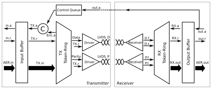
The central mechanism is LEDR (Level-Encoded Dual-Rail) encoding combined with token-ring serializers on both transmitter and receiver. LEDR sends each bit on a data rail and a parity rail, alternating phases so that the receiver can tell bit boundaries by whether the two rails are equal; this makes the protocol delay-insensitive and removes the need for a forwarded clock. The transmitter token-ring encodes parallel event bits into LEDR order, the receiver token-ring decodes them back, and a tunable delay in the transmitter token-ring enforces the timing assumption that the receiver ring can consume each bit within one transmitter bit cycle. Instant on/off is achieved by pulling the LVDS common-mode voltage to ground between events, which switches off the receiver amplifier, and restoring it to a reference voltage at the start of an event.
What would settle it
Measure the bit-error rate of the link while sweeping the tunable delay and the supply voltage and temperature, and observe at what margin bits start being dropped, especially at the wake-up edge when the common-mode voltage is still recovering; a failure at a specific delay would show that the RX-token-ring throughput assumption is not robust.
Extended reading notes
Core claim
The central claim is that a clock-less LEDR-based bit-serial LVDS link can deliver high event throughput while making power strictly event-rate-dependent. Using two LVDS pairs (data and parity) with four-phase handshaking and token-ring serializers, the design avoids any CDR, PLL, or DLL: bit boundaries are recovered from the D=P versus D≠P relation of LEDR. The paper reports measured results from a 0.18 µm CMOS test chip: 1.5 Gbps bit rate, 35.7 MEvents/s for 32-bit events, 31 ns chip-to-chip latency, sub-0.5 ns wake-up/sleep, 0.14 mm² area, and a leakage-dominated idle current floor of 80 nA on the transmitter and 42 nA on the receiver, with linear power scaling down to a sub-µA level around 1k events/s.
Load-bearing premise
The design assumes the receiver token-ring can always absorb each transmitted bit within the transmitter's bit cycle, and this is guaranteed only by a tunable delay in the transmitter; the paper does not measure how much timing margin remains across supply voltage, temperature, and process corners.
Editorial extensions
If this is right
- Multi-chip neuromorphic systems could replace wide parallel AER buses with a single bit-serial link, cutting pin count and I/O area.
- Because power scales with event rate, sparse event traffic—the typical case in neural systems—costs almost nothing, with idle current in the tens of nanoamps.
- The 31 ns chip-to-chip latency and sub-0.5 ns wake-up mean there is no lock-recovery wait for each event burst.
- The compact 0.14 mm² block could be tiled as a building block in core-to-core or chip-to-chip routers.
- The full-rate, non-return-to-zero nature of LEDR allows 1.5 Gbps without a clock, higher than the 0.64 Gbps of a comparable previous AER bit-serial link under test.
Reading between the lines
- If the timing margin of the token-ring handoffs is the real constraint, the same architecture should scale to smaller CMOS nodes only if the tunable delay can track process variations; this can be tested by measuring bit-error rate versus the delay setting.
- The common-mode instant on/off trick could be reused in other low-duty-cycle serial links beyond AER, such as wireline sensor networks, since it converts standby power into leakage only.
- A direct comparison against a clocked CDR link at equal bit rate and same process would quantify how much area and power the CDR actually costs; the paper notes such figures are missing from the prior designs it compares against.
- One could extend the design to variable bit widths or flit-level control flow by adding more token-cells, without changing the encoding.
Signed reviews
Editorial analysis
A structured set of objections, weighed in public.
Referee Report
Summary. The paper presents a clock-less, fully asynchronous bit-serial LVDS link for Address-Event Representation (AER) multi-chip systems. The link is built on Level-Encoded Dual-Rail (LEDR) encoding and token-ring transmitter/receiver architectures, and it avoids conventional CDR blocks with PLL/DLL circuits. A prototype fabricated in 0.18 um CMOS occupies 0.14 mm^2. The authors report a 1.5 Gbps bit rate, an event rate of 35.7 MEvents/s for 32-bit events, and rate-dependent power consumption with a low-rate floor of 80 nA for the transmitter and 42 nA for the receiver. The central claim is that the proposed link is the first such AER bit-serial LVDS interface with no CDR/PLL/DLL, instant on/off, and power that scales linearly with event rate.
Significance. If the timing robustness is established, this is a significant contribution to neuromorphic multi-chip interfacing: it demonstrates a compact 0.14 mm^2, fully asynchronous bit-serial LVDS link without CDR/PLL/DLL, with measured sub-uA idle power and a large dynamic power range. The power-versus-rate curve is a designed architectural property and is verified by measurement, not extracted as a fit to the data, so there is no circularity in the power claim. However, the headline data-rate and event-rate claims are not yet backed by a direct measure of data integrity, and one internal inconsistency in the headline current numbers needs to be resolved before the results can be fully trusted.
major comments (2)
- [II.D and IV] The headline rate claim rests on the unverified assumption stated in Section II.D that the RX token-ring always has higher throughput than the TX token-ring, enforced only by the tunable delay td. The paper reports no bit-error-rate (BER) measurement, no sweep of td around the nominal 0.67 ns bit cycle, no jitter or eye-diagram data, and no process/voltage/temperature corner characterization. The acknowledge signal out.a is a per-word handshake and does not verify that every bit was sampled with the correct value, so the 1.5 Gbps / 35.7 MEvents/s claim is not yet backed by an end-to-end data-integrity metric. Please add a BER measurement over a statistically meaningful number of bits, a td margin sweep, and at least a statement of the measured timing margin.
- [Abstract and Section IV] The two most prominent numerical claims are internally inconsistent: the abstract assigns 19.3 mA to the receiver and 3.57 mA to the transmitter, while Section IV states the opposite. Table I's Pmax value of 22.9 mA is the sum of the two and does not disambiguate the assignment. Please correct the order and ensure that the abstract, Section IV, and Table I all report the same block-level current consumption.
minor comments (5)
- [II.A] The displayed equations for the LEDR encoding are printed with the odd-phase and even-phase cases identical because the overbars are missing; as printed they contradict the prose that specifies the parity rail as the inverted bit value in the even phase. Please restore the overbars so the definition is unambiguous.
- [I and IV] The introduction claims 'Sub-nW (220nW) static power consumption', but 220 nW is sub-uW, not sub-nW. The measured 80 nA plus 42 nA at 1.8 V gives approximately 220 nW, so the label should be corrected to sub-uW.
- [IV] The measurement methodology for the current/power values in Figure 16 is not described. Please state how the supply currents were measured, which blocks were included, the averaging window, and the number of measurements, and add error bars or measurement precision.
- [IV] The paper states that the peak event rate is 'the peak event rate that can be achieved in our experimental setup'; please clarify whether the link itself or the test setup (neural array, router, or pipelining control queue) is the limiting element, and how the 28 ns event period relates to the 25.6 ns active transmission time for a 32-bit event.
- [Table I and II] The relationship between the 1.5 Gbps bit rate, 32-bit events, and 35.7 MEvents/s event rate is not explicitly defined. A 32-bit payload at 1.5 Gbps would nominally take about 21.3 ns, while the measured period is 28 ns; the difference should be explained in terms of protocol overhead, wake-up time, and handshake timing.
Circularity Check
No significant circularity: the central claims are supported by direct chip measurements, with self-citations confined to background context.
full rationale
The paper's central claims are empirical demonstrations on a fabricated 0.18 µm CMOS chip: a 1.5 Gbps bit rate, a 35.7 MEvents/s event rate, and rate-dependent power consumption with sub-µA floors. These numbers come from oscilloscope captures and power measurements, not from a derivation that fits the target. The LEDR encoding and token-ring architecture are adopted from prior work ([15] and [16]), and self-citations to the authors' earlier systems appear only as background motivation or application context, not as load-bearing justification for the new link's performance. The statement that the RX token-ring is required to have the highest throughput and that a tunable delay Td enforces this timing assumption is a design constraint, not a circular reduction. The power-versus-rate curve is a designed property of the clock-less architecture and is verified by measurement; no fitted parameter is renamed as a prediction. The absence of a BER measurement or PVT corner sweep is a robustness concern, but it is a correctness/validation gap, not circularity. The comparison against external implementations in Table I is independent evidence. Overall, no step in the paper reduces by construction to its own inputs.
Assumptions & free parameters
free parameters (2)
- bit cycle delay td =
0.67 ns
- LVDS common-mode reference Vref =
about 1 V
assumptions (4)
- domain assumption LEDR is a delay-insensitive protocol: bit boundaries are recoverable from D=P versus D≠P on two rails.
- ad hoc to paper The RX token-ring is always faster than the TX token-ring, enforced by tunable delay Td.
- domain assumption When common-mode voltage returns to Vref with D=P, the NMOS-input LVDS receiver is fully turned on and ignores spurious repeated LSBs.
- domain assumption Token cells are mutually exclusive and each cell is disabled only by its successor.
Cite this review
Pith. "Pith review of A clock-less ultra-low power bit-serial LVDS link for Address-Event multi-chip systems." pith.science (2026). https://pith.science/paper/2ENDY3VC
@misc{pith2026190806532,
  author       = {Pith},
  title        = {Pith review of: A clock-less ultra-low power bit-serial LVDS link for Address-Event multi-chip systems},
  year         = {2026},
  howpublished = {\url{https://pith.science/paper/2ENDY3VC}},
  note         = {Machine review of arXiv:1908.06532}
}
read the original abstract
We present a power efficient clock-less fully asynchronous bit-serial Low Voltage Differential Signaling (LVDS) link with event-driven instant wake-up and self-sleep features, optimized for high speed inter-chip communication of asynchronous address-events between neuromorphic chips. The proposed LVDS link makes use of the Level-Encoded Dual-Rail (LEDR) representation and a token-ring architecture to encode and transmit data, avoiding the use of conventional large ClockData Recovery (CDR) modules with power-hungry DLL or PLL circuits. We implemented the LVDS circuits in a device fabricated with a standard 0.18 um CMOS process. The total silicon area used for such block is of 0.14 mm^2. We present experimental measurement results to demonstrate that, with a bit rate of 1.5 Gbps and an event width of 32-bit, the proposed LVDS link can achieve transmission event rates of 35.7 M Events/second with current consumption of 19.3 mA and 3.57 mA for receiver and transmitter blocks, respectively. Given the clock-less and instant on/off design choices made, the power consumption of the whole link depends linearly on the data transmission rate. We show that the current consumption can go down to sub-uA for low event rates (e.g., <1k Events/second), with a floor of 80 nA for transmitter and 42 nA for receiver, determined mainly by static off-leakage currents.
Figures


Figures from the paper (11 more)


Reference graph
Works this paper leans on
-
[1]
S. Moradi, N. Qiao, F. Stefanini, and G. Indiveri, “A scalable multicore architecture with heterogeneous memory structures for dynamic neuromorphic asynchronous processors (DYNAPs),”Biomedical Circuits and Systems, IEEE Transactions on, pp. 1–17, 2017
work page 2017
-
[2]
Hierarchical address event routing for reconfigurable large-scale neuromorphic sys- tems,
J. Park, T. Yu, S. Joshi, C. Maier, and G. Cauwenberghs, “Hierarchical address event routing for reconfigurable large-scale neuromorphic sys- tems,”IEEE Transactions on Neural Networks and Learning Systems, pp. 1–15, 2016
work page 2016
-
[3]
A million spiking-neuron integrated circuit with a scalable communication network and interface,
P. A. Merolla, J. V. Arthur, R. Alvarez-Icaza, A. S. Cassidy, J. Sawada, F. Akopyan, B. L. Jackson, N. Imam, C. Guo, Y. Nakamura, B. Brezzo, I. Vo, S. K. Esser, R. Appuswamy, B. Taba, A. Amir, M. D. Flickner, W. P. Risk, R. Manohar, and D. S. Modha, “A million spiking-neuron integrated circuit with a scalable communication network and interface,” Science,...
work page 2014
-
[4]
The SpiNNaker project,
S. Furber, F. Galluppi, S. Temple, and L. Plana, “The SpiNNaker project,” Proceedings of the IEEE, vol. 102, no. 5, pp. 652–665, May 2014
2014
-
[5]
Neurogrid: A mixed-analog-digital multichip system for large-scale neural simulations,
B. V. Benjamin, P. Gao, E. McQuinn, S. Choudhary, A. R. Chan- drasekaran, J. Bussat, R. Alvarez-Icaza, J. Arthur, P. Merolla, and K. Boahen, “Neurogrid: A mixed-analog-digital multichip system for large-scale neural simulations,”Proceedings of the IEEE, vol. 102, no. 5, pp. 699–716, 2014
2014
-
[6]
S.-C. Liu, T. Delbruck, G. Indiveri, A. Whatley, and R. Douglas,Event- based neuromorphic systems. Wiley, 2014
work page 2014
-
[7]
S.-C. Liu and T. Delbruck, “Neuromorphic sensory systems,”Current Opinion in Neurobiology, vol. 20, no. 3, pp. 288–295, 2010
work page 2010
-
[8]
N. Qiao, H. Mostafa, F. Corradi, M. Osswald, F. Stefanini, D. Sumislawska, and G. Indiveri, “A re-configurable on-line learning spiking neuromorphic processor comprising 256 neurons and 128k synapses,”Frontiers in Neuroscience, vol. 9, no. 141, 2015
work page 2015
Show all 19 references
-
[9]
Robust working memory in an asynchronously spiking neural network realized in neuromorphic VLSI,
M. Giulioni, P. Camilleri, M. Mattia, V. Dante, J. Braun, and P. D. Giudice, “Robust working memory in an asynchronously spiking neural network realized in neuromorphic VLSI,”Frontiers in Neuroscience, vol. 5, no. 149, 2012
2012
-
[10]
Synthesizing cognition in neuromorphic electronic systems,
E. Neftci, J. Binas, U. Rutishauser, E. Chicca, G. Indiveri, and R. Douglas, “Synthesizing cognition in neuromorphic electronic systems,” Proceedings of the National Academy of Sciences, vol. 110, no. 37, pp. E3468–E3476, 2013
2013
-
[11]
CAVIAR: A 45k neuron, 5M synapse, 12G connects/s aer hardware sensory– processing– learning–actuating system for high-speed visual object recognition and tracking,
R. Serrano-Gotarredona, M. Oster, P. Lichtsteiner, A. Linares- Barranco, R. Paz-Vicente, F. Gómez-Rodriguez, L. Camunas-Mesa, R. Berner, M. Rivas-Perez, T. Delbruck, S.-C. Liu, R. Douglas, P. Häfliger, G. Jimenez-Moreno, A. Civit-Ballcels, T. Serrano- Gotarredona, A. Acosta-Jim...
2009
-
[12]
A multi-chip pulse-based neuromorphic infrastructure and its application to a model of orientation selectivity,
E. Chicca, A. Whatley, P. Lichtsteiner, V. Dante, T. Delbruck, P. Del Giudice, R. Douglas, and G. Indiveri, “A multi-chip pulse-based neuromorphic infrastructure and its application to a model of orientation selectivity,”IEEE Transactions on Circuits and Systems I, vol. 5, no....
2007
-
[13]
A 240×180 130 dB 3µs latency global shutter spatiotemporal vision sensor,
C. Brandli, R. Berner, M. Yang, S.-C. Liu, and T. Delbruck, “A 240×180 130 dB 3µs latency global shutter spatiotemporal vision sensor,”IEEE Journal of Solid-State Circuits, vol. 49, no. 10, pp. 2333–2341, 2014
2014
-
[14]
A 1.5ns OFF/ON switching-time voltage-mode LVDS driver/receiver pair for asynchronous AER bit-serial chip grid links with up to 40 times event-rate dependent power savings,
C. Zamarreño-Ramos, R. Kulkarni, J. Silva-Martínez, T. Serrano- Gotarredona, and B. Linares-Barranco, “A 1.5ns OFF/ON switching-time voltage-mode LVDS driver/receiver pair for asynchronous AER bit-serial chip grid links with up to 40 times event-rate dependent power savings,” ...
2013
-
[15]
Efficient self-timing with level-encoded 2-phase dual-rail (LEDR),
M. E. Dean, T. E. Williams, and D. L. Dill, “Efficient self-timing with level-encoded 2-phase dual-rail (LEDR),” inProceedings of the 1991 University of California/Santa Cruz conference on Advanced research in VLSI. MIT Press, 1991, pp. 55–70
1991
-
[16]
A high-speed clockless serial link transceiver,
J. Teifel and R. Manohar, “A high-speed clockless serial link transceiver,” in Asynchronous Circuits and Systems, 2003. Proceedings. Ninth Inter- national Symposium on. IEEE, 2003, pp. 151–161
2003
-
[17]
A0.35 µm sub-ns wake-up time ON-OFF switchable LVDS driver- receiver chip I/O pad pair for rate-dependent power saving in AER bit-serial links,
C. Zamarreno-Ramos, T. Serrano-Gotarredona, and B. Linares-Barranco, “A0.35 µm sub-ns wake-up time ON-OFF switchable LVDS driver- receiver chip I/O pad pair for rate-dependent power saving in AER bit-serial links,”Biomedical Circuits and Systems, IEEE Transactions on, vol. 6, ...
2012
-
[18]
LVDS interface for aer links with burst mode operation capability,
C. Zamarreno-Ramos, R. Serrano-Gotarredona, T. Serrano-Gotarredona, and B. Linares-Barranco, “LVDS interface for aer links with burst mode operation capability,” inCircuits and Systems, 2008. ISCAS 2008. IEEE International Symposium on. IEEE, 2008, pp. 644–647
2008
-
[19]
Memory and information processing in neuromorphic systems,
G. Indiveri, and S.-C. Liu, “Memory and information processing in neuromorphic systems,” inProceedings of IEEE, vol. 103, no. 8, pp. 1379–1397, 2015
2015
Reviewed August 14, 2026 · model on record in the stance chip above.
Discussion (0). Continue with ORCID to comment.