REVIEW 5 major objections 4 minor 45 references
Tunable Giant Rashba-type Spin Splitting in PtSe$_2$/MoSe$_2$ Heterostructure
T0 review · 5 major / 4 minor · reviewed 2026-08-14 · deepseek-v4-flash
Pith's one-line read Stacking PtSe2 on MoSe2 creates a 110 meV Rashba spin splitting that strain and an electric field can tune.
desk verdict Solid DFT prediction of a large tunable Rashba splitting in a PtSe2/MoSe2 heterostructure, but the headline numbers rest on one idealized stacking geometry that the paper does not test. read the letter →
The pith
A machine-rendered reading of the paper's core claim, the machinery that carries it, and where it could break.
The reading
What carries the argument
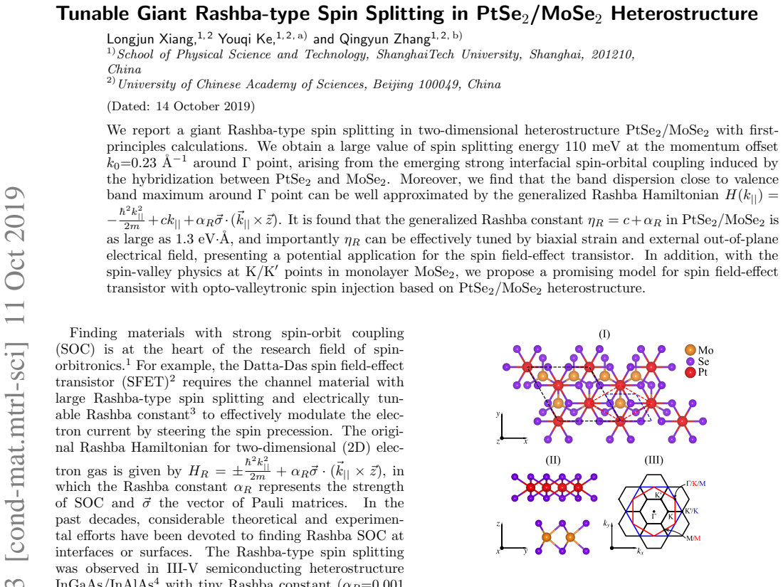
The load-bearing object is the commensurate heterostructure supercell: a $\sqrt{3}\times\sqrt{3}$ PtSe2 layer stacked on a $2\times2$ MoSe2 layer, an interface that breaks inversion symmetry. The microscopic generator of the effect is the interlayer hybridization near the valence-band edge at Γ between Mo-d orbitals of MoSe2, mainly $d_{z^2}$, and Se-p orbitals of PtSe2, mainly $p_z$; this hybridization makes the vertical charge distribution asymmetric and produces an effective electric field that activates strong spin-orbit coupling. The analytic carrier of the argument is the generalized Rashba Hamiltonian, in which the linear term $c k_{\parallel}$ captures the spin-independent 'sombrero hat' crystal-field dispersion and the term $\alpha_R \vec{\sigma}\cdot(\vec{k}_{\parallel}\times\vec{z})$ captures the Rashba coupling. Their sum, $\eta_R=c+\alpha_R$, enters the differential spin-precession phase $\Delta\theta = 2m\eta_R L/\hbar^2$, connecting the fitted band parameter directly to the proposed transistor's operation.
What would settle it
Spin- and angle-resolved photoemission on a PtSe2/MoSe2 stack would settle the claim: if no in-plane helical spin-split band appears around Γ with a splitting near 110 meV at $k_0\approx0.23$ Å$^{-1}$, and if the band parameter $\eta_R$ does not shift by roughly 24% under an applied out-of-plane field of ±1.5 V/nm, the central prediction is contradicted.
Extended reading notes
Core claim
The central claim is that the PtSe2/MoSe2 van der Waals heterostructure hosts a tunable, large Rashba-type spin splitting that neither constituent monolayer exhibits on its own. In the density-functional band structure with spin-orbit coupling, the two highest valence bands around Γ take a 'sombrero hat' form that is well described by the generalized Rashba Hamiltonian $H(k_{\parallel})=-\frac{\hbar^2 k_{\parallel}^2}{2m}+c k_{\parallel}+\alpha_R \vec{\sigma}\cdot(\vec{k}_{\parallel}\times \vec{z})$. The fit gives a momentum offset $k_0=0.23$ Å$^{-1}$, a generalized Rashba energy $E_R=150$ meV, a spin splitting of 110 meV at $k_0$, and $\eta_R=c+\alpha_R=1.3$ eV·Å, estimated as $2E_R/k_0$. The in-plane helical spin texture confirms the Rashba character. Biaxial strain from −1.5% to +1.5% changes $\eta_R$ from 1.62 to 1.00 eV·Å, and an out-of-plane electric field of ±1.5 V/nm changes it from 1.46 to 1.18 eV·Å, a change of about 24%. Tensile strain can also raise the Γ valence-band maximum above the K-point one by about 0.1 eV, creating an energy window populated only by Rashba-type states. The authors conclude that the system is a promising platform for a spin field-effect transistor, with a minimum channel length of about 7.1 nm estimated from the field-induced change in $\eta_R$.
Load-bearing premise
The calculation assumes the idealized commensurate stacking of the two monolayers, with its relaxed interlayer spacing, faithfully represents a real PtSe2/MoSe2 interface, and that the chosen density functional correctly places the Γ and K valence states relative to one another; a different twist, spacing, or strain could weaken the hybridization and shrink the predicted splitting.
Editorial extensions
If this is right
- Light hole doping in the energy window from 0 to −0.1 eV around Γ gives access to a single upper Rashba-split band, so transport can pass through one helical spin channel without competing valley states.
- Because the differential precession phase $\Delta\theta=2m\eta_R L/\hbar^2$ does not depend on carrier energy within this window, a spin transistor built on this band would not be broadened by the energy spread of the injected carriers.
- Applying +1.5% tensile strain raises the Γ valence-band maximum relative to the K-point maximum by about 0.1 eV, producing an operating window in which only the Rashba-type states are available.
- The out-of-plane electric field changes $\eta_R$ by about 24% over the range ±1.5 V/nm, providing a gate-voltage handle on spin precession, and the estimated channel length for full spin flip under that tuning is about 7.1 nm.
Reading between the lines
- The paper tests one commensurate registry; the same Mo-d/Se-p hybridization mechanism suggests that twisted or Janus-engineered interfaces would shift $k_0$ and $\eta_R$ continuously, possibly yielding even larger tunability.
- Since $\eta_R$ mixes a crystal-field term $c$ with the spin-orbit term $\alpha_R$, an experiment that measures the band-minimum shift and the spin splitting separately could separate the two and reveal whether electric-field tuning acts mainly on $c$ through interlayer distance or on $\alpha_R$.
- The clean-window claim, that 0 to −0.1 eV is free of K-point states, is the most sensitive prediction; recomputing the band edges with a higher-level electronic-structure method would show whether the proposed operating window survives beyond the density-functional approximation used here.
- If spin-resolved photoemission confirms the 110 meV splitting, the same interface could be tested in a two-terminal spin-precession device before a full three-terminal transistor is attempted.
Signed reviews
Editorial analysis
A structured set of objections, weighed in public.
Referee Report
Summary. The paper reports first-principles DFT calculations on a PtSe2/MoSe2 van der Waals heterostructure, claiming a giant Rashba-type spin splitting of 110 meV at momentum offset k0=0.23 Å^-1 around the Γ point. The authors introduce a generalized Rashba Hamiltonian, extract a generalized Rashba constant η_R = c + α_R ≈ 1.3 eV·Å, and show that η_R can be tuned by biaxial strain and an external out-of-plane electric field. They further propose a spin field-effect transistor based on this heterostructure, using the valley physics of MoSe2 for spin injection and estimating a minimum channel length of 7.1 nm.
Significance. If validated, the predicted large, electrically tunable Rashba-like splitting near the valence band edge in a TMDC heterostructure would be a significant advance for spin-orbitronics, and the proposed SFET is a concrete application. The paper benefits from a clear spin-texture analysis (in-plane helical polarization), a family-wide comparison in the supplement (PtX2/MX2 with M=Mo,W and X=S,Se,Te), and a transparent derivation of the generalized Rashba model. However, the quantitative claims rest on parameters extracted by visual inspection and on a single idealised interface geometry, so the significance is conditional on robustness checks that are not currently provided.
major comments (5)
- [Supplementary Sections II and IV; Eqs. (S6)-(S8)] The channel-length estimate uses m = 0.81 m_e, but the generalized Rashba dispersion E = -ℏ²k²/(2m) + η_R k has its extremum at k0 = mη_R/ℏ². With the reported k0 = 0.23 Å⁻¹ and η_R = 1.3 eV·Å, one obtains m ≈ 1.35 m_e, not 0.81 m_e. This internal inconsistency directly affects the predicted L = 7.1 nm (Supplementary Section IV). Please recalculate with a consistent set of parameters or clarify how m was obtained.
- [Fig. 3(I) and Supplementary Fig. S1(II)] ER = 150 meV and k0 = 0.23 Å⁻¹, and hence η_R = 1.3 eV·Å, are extracted by visual inspection of a band plot, and the agreement between the generalized Rashba Hamiltonian and the DFT bands is only shown graphically. A quantitative least-squares fit with residuals and uncertainty estimates is needed to support the quantitative claims, especially since the model parameters are used for the device estimate.
- [Abstract and text after Eq. (1)] The spin splitting at k0 is 110 meV, which for k0 = 0.23 Å⁻¹ yields α_R = ΔE/(2k0) ≈ 0.24 eV·Å. The reported η_R = c + α_R ≈ 1.3 eV·Å is therefore dominated by the spin-independent crystal-field term c. Comparing η_R with literature Rashba constants (e.g., BiTeI, GeTe) is misleading. The authors should report α_R and c separately and qualify the 'one of the largest' statement.
- [Fig. 2(VII) and Supplementary Fig. S3] The giant splitting is attributed to Mo-d/Se-p interfacial hybridization, which is exponentially sensitive to interlayer distance and lateral stacking. The supplement shows that PtTe2/MoTe2, with a larger interlayer distance, exhibits essentially no p-d hybridization or splitting. Since only a single commensurate stacking is studied for PtSe2/MoSe2, the robustness of the 110 meV and 1.3 eV·Å values to realistic interface variations is untested. Alternative stackings and a range of interlayer distances should be examined or justified.
- [Fig. 4 and the proposed SFET] The SFET proposal relies on a ~0.1 eV energy window where the Γ-point Rashba-split band lies above the K-point valence states. The relative Γ/K ordering and ΔE are computed with PBE-D3, which is known to have sizable errors for TMDC band alignments. Since Fig. 4 shows ΔE close to zero for several strain/electric-field conditions, small functional errors could change the device operation. A check with a more accurate functional (e.g., HSE06 or GW) for the key configurations would strengthen the device claim.
minor comments (4)
- [Eq. (1)] The term c k_|| should be written as c |k_||| to make the rotational invariance explicit; as written, c k_|| is ambiguous.
- [Fig. 3(I)] The caption of Fig. 3(I) should define ER, k0, and the constant-energy cut in the panel.
- [Supplementary Eq. (S5)] The spinors in Eq. (S5) are not normalized; please add the 1/√2 factor or state explicitly that they are unnormalized.
- [Abstract and Fig. 3(I)] The relation between the 110 meV spin splitting at k0 and ER = 150 meV should be stated explicitly, since for a reader familiar with standard Rashba models the two numbers may appear inconsistent.
Circularity Check
No significant circularity: the reported Rashba parameters are read from DFT band structures, and the SFET estimate is an explicit application, not an independent prediction.
full rationale
The central derivation is a DFT calculation: the authors build a commensurate PtSe2/MoSe2 supercell, relax it with PBE-D3, and compute band structures with SOC. The giant spin splitting (110 meV, k0=0.23 Å^-1) is read directly from those bands. The generalized Rashba Hamiltonian H(k||) = -hbar^2 k||^2/2m + c k|| + alpha_R sigma dot (k|| x z) is introduced as a two-parameter fit to the two valence bands near Gamma, with c and alpha_R chosen to reproduce the DFT dispersion; eta_R = 2E_R/k0 is then simply the ratio read from the same band structure. This is parameter extraction from first-principles data, not a prediction derived from the fit and then compared back to the same data. The tunability under strain and electric field is obtained by recomputing the DFT bands at different geometries and fields; each eta_R value is again read from the corresponding band structure, so there is no fitted-input-called-prediction loop. The SFET channel length estimate uses the extracted eta_R values in the standard Datta-Das formula, and the paper explicitly labels it as an estimate rather than an independent validation. The only potentially self-referential citation, Q. Zhang and U. Schwingenschlögl, Phys. Rev. B 97, 155415 (2018), appears in the introduction as one example among several previous Rashba predictions and is not load-bearing for the present derivation. No uniqueness theorem is invoked, and no ansatz is imported solely from the authors' prior work. Therefore no circular step is present.
Assumptions & free parameters
free parameters (6)
- ηR (generalized Rashba constant) =
1.3 eV·Å (equilibrium); varies from 1.00 to 1.62 eV·Å under strain
- ER (generalized Rashba energy) =
150 meV
- k0 (momentum offset) =
0.23 Å^-1
- c (linear spin-independent coefficient) =
not given separately; c = ηR - αR
- αR (Rashba coefficient) =
inferred ≈0.24 eV·Å (since 2αR k0 = 110 meV at k0=0.23 Å^-1)
- effective mass m =
0.81 me (average)
assumptions (3)
- domain assumption PBE-GGA DFT with PAW and DFT-D3 yields quantitatively reliable band structures and spin splittings for PtSe2/MoSe2.
- domain assumption The single commensurate supercell (√3×√3 PtSe2 on 2×2 MoSe2) accurately represents the physical heterostructure.
- ad hoc to paper The generalized Rashba Hamiltonian (Eq. 1) is a valid effective description of the valence band edge from about -0.1 eV to 0 eV.
Cite this review
Pith. "Pith review of Tunable Giant Rashba-type Spin Splitting in PtSe$_2$/MoSe$_2$ Heterostructure." pith.science (2026). https://pith.science/paper/25V4CRN2
@misc{pith2026190806689,
  author       = {Pith},
  title        = {Pith review of: Tunable Giant Rashba-type Spin Splitting in PtSe$_2$/MoSe$_2$ Heterostructure},
  year         = {2026},
  howpublished = {\url{https://pith.science/paper/25V4CRN2}},
  note         = {Machine review of arXiv:1908.06689}
}
abstract
We report a giant Rashba-type spin splitting in two-dimensional heterostructure PtSe$_2$/MoSe$_2$ with first-principles calculations. We obtain a large value of spin splitting energy 110 meV at the momentum offset $k_0$=0.23 \AA$^{-1}$ around $\mathrm{\Gamma}$ point, arising from the emerging strong interfacial spin-orbital coupling induced by the hybridization between PtSe$_2$ and MoSe$_2$. Moreover, we find that the band dispersion close to valence band maximum around $\Gamma$ point can be well approximated by the generalized Rashba Hamiltonian $H(k_{||})=-\frac{\hbar^2 k_{||}^2}{2m}+c k_{||}+\alpha_R \vec{\sigma}\cdot(\vec{k}_{||} \times \vec{z})$. It is found that the generalized Rashba constant $\eta_R=c+\alpha_R$ in PtSe$_2$/MoSe$_2$ is as large as 1.3 eV$\cdot\text{\AA}$, and importantly $\eta_R$ can be effectively tuned by biaxial strain and external out-of-plane electrical field, presenting a potential application for the spin field-effect transistor. In addition, with the spin-valley physics at $\mathrm{K}/\mathrm{K}'$ points in monolayer MoSe$_2$, we propose a promising model for spin field-effect transistor with opto-valleytronic spin injection based on PtSe$_2$/MoSe$_2$ heterostructure.
Figures


Figures from the paper (1 more)

Reference graph
Works this paper leans on
-
[1]
author author A. Manchon , author H. C. \ Koo , author J. Nitta , author S. Frolov , \ and\ author R. Duine ,\ title title New perspectives for Rashba spin-orbit coupling , \ @noop journal journal Nature materials \ volume 14 ,\ pages 871 ( year 2015 ) NoStop
work page 2015
-
[2]
author author S. Datta \ and\ author B. Das ,\ title title Electronic analog of the electro‐optic modulator , \ @noop journal journal Applied Physics Letters \ volume 56 ,\ pages 665--667 ( year 1990 ) NoStop
work page 1990
-
[3]
author author Y. A. \ Bychkov \ and\ author \'E . I. \ Rashba ,\ title title Properties of a 2D electron gas with lifted spectral degeneracy , \ @noop journal journal JETP lett \ volume 39 ,\ pages 78 ( year 1984 ) NoStop
work page 1984
-
[4]
author author J. Nitta , author T. Akazaki , author H. Takayanagi , \ and\ author T. Enoki ,\ title title Gate control of spin-orbit interaction in an inverted In _ 0.53 Ga _ 0.47 As / In _ 0.52 Al _ 0.48 As heterostructure , \ @noop journal journal Phys. Rev. Lett. \ volume 78 ,\ pages 1335--1338 ( year 1997 ) NoStop
work page 1997
-
[5]
author author S. LaShell , author B. A. \ McDougall , \ and\ author E. Jensen ,\ title title Spin splitting of an Au (111) surface state band observed with angle resolved photoelectron spectroscopy , \ @noop journal journal Phys. Rev. Lett. \ volume 77 ,\ pages 3419--3422 ( year 1996 ) NoStop
work page 1996
-
[6]
author author Y. M. \ Koroteev , author G. Bihlmayer , author J. E. \ Gayone , author E. V. \ Chulkov , author S. Bl\"ugel , author P. M. \ Echenique , \ and\ author P. Hofmann ,\ title title Strong spin-orbit splitting on Bi surfaces , \ @noop journal journal Phys. Rev. Lett. \ volume 93 ,\ pages 046403 ( year 2004 ) NoStop
work page 2004
-
[7]
author author T. Hirahara , author T. Nagao , author I. Matsuda , author G. Bihlmayer , author E. V. \ Chulkov , author Y. M. \ Koroteev , author P. M. \ Echenique , author M. Saito , \ and\ author S. Hasegawa ,\ title title Role of spin-orbit coupling and hybridization effects in the electronic structure of ultrathin Bi films , \ @noop journal journal Ph...
work page 2006
-
[8]
author author A. Varykhalov , author D. Marchenko , author M. R. \ Scholz , author E. D. L. \ Rienks , author T. K. \ Kim , author G. Bihlmayer , author J. S\'anchez-Barriga , \ and\ author O. Rader ,\ title title Ir (111) surface state with giant Rashba splitting persists under graphene in air , \ @noop journal journal Phys. Rev. Lett. \ volume 108 ,\ pa...
work page 2012
Show all 45 references
-
[9]
author author J. H. \ Dil , author F. Meier , author J. Lobo-Checa , author L. Patthey , author G. Bihlmayer , \ and\ author J. Osterwalder ,\ title title Rashba-type spin-orbit splitting of quantum well states in ultrathin Pb films , \ @noop journal journal Phys. Rev. Lett. \...
2008
-
[10]
author author P. D. C. \ King , author R. C. \ Hatch , author M. Bianchi , author R. Ovsyannikov , author C. Lupulescu , author G. Landolt , author B. Slomski , author J. H. \ Dil , author D. Guan , author J. L. \ Mi , author E. D. L. \ Rienks , author J. Fink , author A. Lind...
2011
-
[11]
\ Zhu , author G
author author Z.-H. \ Zhu , author G. Levy , author B. Ludbrook , author C. N. \ Veenstra , author J. A. \ Rosen , author R. Comin , author D. Wong , author P. Dosanjh , author A. Ubaldini , author P. Syers , author N. P. \ Butch , author J. Paglione , author I. S. \ Elfimov ,...
2011
-
[12]
author author C. R. \ Ast , author J. Henk , author A. Ernst , author L. Moreschini , author M. C. \ Falub , author D. Pacil\'e , author P. Bruno , author K. Kern , \ and\ author M. Grioni ,\ title title Giant spin splitting through surface alloying , \ @noop journal journal P...
2007
-
[13]
Gierz , author T
author author I. Gierz , author T. Suzuki , author E. Frantzeskakis , author S. Pons , author S. Ostanin , author A. Ernst , author J. Henk , author M. Grioni , author K. Kern , \ and\ author C. R. \ Ast ,\ title title Silicon surface with giant spin splitting , \ @noop journa...
2009
-
[14]
author author J. R. \ Bindel , author M. Pezzotta , author J. Ulrich , author M. Liebmann , author E. Y. \ Sherman , \ and\ author M. Morgenstern ,\ title title Probing variations of the Rashba spin--orbit coupling at the nanometre scale , \ @noop journal journal Nature Physic...
2016
-
[15]
Ishizaka , author M
author author K. Ishizaka , author M. S. \ Bahramy , author H. Murakawa , author M. Sakano , author T. Shimojima , author T. Sonobe , author K. Koizumi , author S. Shin , author H. Miyahara , author A. Kimura , author K. Miyamoto , author T. Okuda , author H. Namatame , author...
2011
-
[16]
Di Sante , author P
author author D. Di Sante , author P. Barone , author R. Bertacco , \ and\ author S. Picozzi ,\ title title Electric control of the giant Rashba effect in bulk GeTe , \ @noop journal journal Advanced Materials \ volume 25 ,\ pages 509--513 ( year 2013 ) NoStop
2013
-
[17]
Liebmann , author C
author author M. Liebmann , author C. Rinaldi , author D. Di Sante , author J. Kellner , author C. Pauly , author R. N. \ Wang , author J. E. \ Boschker , author A. Giussani , author S. Bertoli , author M. Cantoni , et al. ,\ title title Giant Rashba -type spin splitting in fe...
2016
-
[18]
Ma , author Y
author author Y. Ma , author Y. Dai , author W. Wei , author X. Li , \ and\ author B. Huang ,\ title title Emergence of electric polarity in BiTeX ( X = Br and I ) monolayers and the giant Rashba spin splitting , \ @noop journal journal Physical Chemistry Chemical Physics \ vo...
2014
-
[19]
Ajayan , author P
author author P. Ajayan , author P. Kim , \ and\ author K. Banerjee ,\ title title Two-dimensional van der Waals materials , \ @noop journal journal Physics Today \ volume 69 ,\ pages 38--44 ( year 2016 ) NoStop
2016
-
[20]
author author K. S. \ Novoselov , author A. Mishchenko , author A. Carvalho , \ and\ author A. H. \ Castro Neto ,\ title title 2D materials and van der Waals heterostructures , \ @noop journal journal Science \ volume 353 ,\ pages aac9439 ( year 2016 ) NoStop
2016
-
[21]
Kasai , author K
author author H. Kasai , author K. Tolborg , author M. Sist , author J. Zhang , author V. R. \ Hathwar , author M. . \ Fils , author S. Cenedese , author K. Sugimoto , author J. Overgaard , author E. Nishibori , et al. ,\ title title X-ray electron density investigation of che...
2018
-
[22]
Liu , author Y
author author Q. Liu , author Y. Guo , \ and\ author A. J. \ Freeman ,\ title title Tunable Rashba effect in two-dimensional LaOBiS _2 films: Ultrathin candidates for spin field effect transistors , \ @noop journal journal Nano letters \ volume 13 ,\ pages 5264--5270 ( year 20...
2013
-
[23]
Singh \ and\ author A
author author S. Singh \ and\ author A. H. \ Romero ,\ title title Giant tunable rashba spin splitting in a two-dimensional BiSb monolayer and in BiSb / AlN heterostructures , \ @noop journal journal Phys. Rev. B \ volume 95 ,\ pages 165444 ( year 2017 ) NoStop
2017
-
[24]
\ Wang \ and\ author H.-T
author author T.-H. \ Wang \ and\ author H.-T. \ Jeng ,\ title title Wide-range ideal 2D Rashba electron gas with large spin splitting in Bi _2 Se _3 / MoTe _2 heterostructure , \ @noop journal journal npj Comput. Mater. \ volume 3 ,\ pages 5--10 ( year 2017 ) NoStop
2017
-
[25]
Zhang \ and\ author U
author author Q. Zhang \ and\ author U. Schwingenschl\"ogl ,\ title title Rashba effect and enriched spin-valley coupling in GaX / MX _2 ( M = Mo , W ; X = S , Se , Te ) heterostructures , \ @noop journal journal Phys. Rev. B \ volume 97 ,\ pages 155415 ( year 2018 ) NoStop
2018
-
[26]
Wang , author L
author author Y. Wang , author L. Li , author W. Yao , author S. Song , author J. T. \ Sun , author J. Pan , author X. Ren , author C. Li , author E. Okunishi , author Y.-Q. \ Wang , author E. Wang , author Y. Shao , author Y. Y. \ Zhang , author H.-t. \ Yang , author E. F. \ ...
2015
-
[27]
Zhao , author J
author author Y. Zhao , author J. Qiao , author Z. Yu , author P. Yu , author K. Xu , author S. P. \ Lau , author W. Zhou , author Z. Liu , author X. Wang , author W. Ji , et al. ,\ title title High-electron-mobility and air-stable 2D layered PtSe _2 FET s , \ @noop journal jo...
2017
-
[28]
Yao , author E
author author W. Yao , author E. Wang , author H. Huang , author K. Deng , author M. Yan , author K. Zhang , author K. Miyamoto , author T. Okuda , author L. Li , author Y. Wang , et al. ,\ title title Direct observation of spin-layer locking by local Rashba effect in monolaye...
2017
-
[29]
Zhang , author Q
author author X. Zhang , author Q. Liu , author J.-W. \ Luo , author A. J. \ Freeman , \ and\ author A. Zunger ,\ title title Hidden spin polarization in inversion-symmetric bulk crystals , \ @noop journal journal Nature Physics \ volume 10 ,\ pages 387 ( year 2014 ) NoStop
2014
-
[30]
Yuan , author Q
author author L. Yuan , author Q. Liu , author X. Zhang , author J.-W. \ Luo , author S.-S. \ Li , \ and\ author A. Zunger ,\ title title Uncovering and tailoring hidden Rashba spin--orbit splitting in centrosymmetric crystals , \ @noop journal journal Nature communications \ ...
2019
-
[31]
author author M. A. U. \ Absor , author I. Santoso , author Harsojo , author K. Abraha , author H. Kotaka , author F. Ishii , \ and\ author M. Saito ,\ title title Strong Rashba effect in the localized impurity states of halogen-doped monolayer PtSe _ 2 , \ @noop journal journ...
2018
-
[32]
\ Chang , author W
author author Y.-H. \ Chang , author W. Zhang , author Y. Zhu , author Y. Han , author J. Pu , author J.-K. \ Chang , author W.-T. \ Hsu , author J.-K. \ Huang , author C.-L. \ Hsu , author M.-H. \ Chiu , et al. ,\ title title Monolayer MoSe _2 grown by chemical vapor depositi...
2014
-
[33]
Reyes-Retana \ and\ author F
author author J. Reyes-Retana \ and\ author F. Cervantes-Sodi ,\ title title Spin-orbital effects in metal-dichalcogenide semiconducting monolayers , \ @noop journal journal Scientific reports \ volume 6 ,\ pages 24093 ( year 2016 ) NoStop
2016
-
[34]
Kresse \ and\ author D
author author G. Kresse \ and\ author D. Joubert ,\ title title From ultrasoft pseudopotentials to the projector augmented-wave method , \ @noop journal journal Phys. Rev. B \ volume 59 ,\ pages 1758--1775 ( year 1999 ) NoStop
1999
-
[35]
author author J. P. \ Perdew , author K. Burke , \ and\ author M. Ernzerhof ,\ title title Generalized gradient approximation made simple , \ @noop journal journal Phys. Rev. Lett. \ volume 77 ,\ pages 3865--3868 ( year 1996 ) NoStop
1996
-
[36]
Grimme , author J
author author S. Grimme , author J. Antony , author S. Ehrlich , \ and\ author H. Krieg ,\ title title A consistent and accurate ab initio parametrization of density functional dispersion correction ( DFT-D ) for the 94 elements H - Pu , \ @noop journal journal The Journal of ...
2010
-
[37]
author author Z. Y. \ Zhu , author Y. C. \ Cheng , \ and\ author U. Schwingenschl\"ogl ,\ title title Giant spin-orbit-induced spin splitting in two-dimensional transition-metal dichalcogenide semiconductors , \ @noop journal journal Phys. Rev. B \ volume 84 ,\ pages 153402 ( ...
2011
-
[38]
Kang , author J
author author J. Kang , author J. Li , author S.-S. \ Li , author J.-B. \ Xia , \ and\ author L.-W. \ Wang ,\ title title Electronic structural moir\' e pattern effects on MoS _2 / MoSe _2 2 D heterostructures , \ @noop journal journal Nano Lett. \ volume 13 ( year 2013 ) NoStop
2013
-
[39]
\ Komsa \ and\ author A
author author H.-P. \ Komsa \ and\ author A. V. \ Krasheninnikov ,\ title title Electronic structures and optical properties of realistic transition metal dichalcogenide heterostructures from first principles , \ @noop journal journal Phys. Rev. B \ volume 88 ,\ pages 085318 (...
2013
-
[40]
Su , author W
author author X. Su , author W. Ju , author R. Zhang , author C. Guo , author J. Zheng , author Y. Yong , \ and\ author X. Li ,\ title title Bandgap engineering of MoS _2 / MX _2 ( MX _2 = WS _2 , MoSe _2 and WSe _2 ) heterobilayers subjected to biaxial strain and normal compr...
2016
-
[41]
author author D. V. \ Rybkovskiy , author A. V. \ Osadchy , \ and\ author E. D. \ Obraztsova ,\ title title Transition from parabolic to ring-shaped valence band maximum in few-layer gas, gase, and inse , \ 10.1103/PhysRevB.90.235302 journal journal Phys. Rev. B \ volume 90 ,\...
-
[42]
Chuang , author S.-C
author author P. Chuang , author S.-C. \ Ho , author L. W. \ Smith , author F. Sfigakis , author M. Pepper , author C.-H. \ Chen , author J.-C. \ Fan , author J. P. \ Griffiths , author I. Farrer , author H. E. \ Beere , author G. A. C. \ Jones , author D. A. \ Ritchie , \ and...
2015
-
[43]
author author Y. K. \ Luo , author J. Xu , author T. Zhu , author G. Wu , author E. J. \ McCormick , author W. Zhan , author M. R. \ Neupane , \ and\ author R. K. \ Kawakami ,\ title title Opto-valleytronic spin injection in monolayer MoS _2 /few-layer graphene hybrid spin val...
2017
-
[44]
note The change of the effective mass m is minor, we use the average value m=0.81 m_e in our estimation. Stop
-
[45]
D. V. Rybkovskiy, A. V. Osadchy, and E. D. Obraztsova, Phys. Rev. B\ 90, 235302 (2014)
2014
Reviewed August 14, 2026 · model on record in the stance chip above.
Discussion (0). Continue with ORCID to comment.