REVIEW 2 major objections 4 minor 32 references
Thermal generation of shift electric current
T0 review · 2 major / 4 minor · reviewed 2026-08-14 · deepseek-v4-flash
Pith's one-line read Cooling a hot electron gas in a low-symmetry quantum well can produce a direct electric current.
desk verdict A plausible new phonogalvanic shift current with a real technical flaw in the central approximation; worth refereeing, but the quantitative result needs an equipartition caveat. read the letter →
The pith
A machine-rendered reading of the paper's core claim, the machinery that carries it, and where it could break.
The reading
What carries the argument
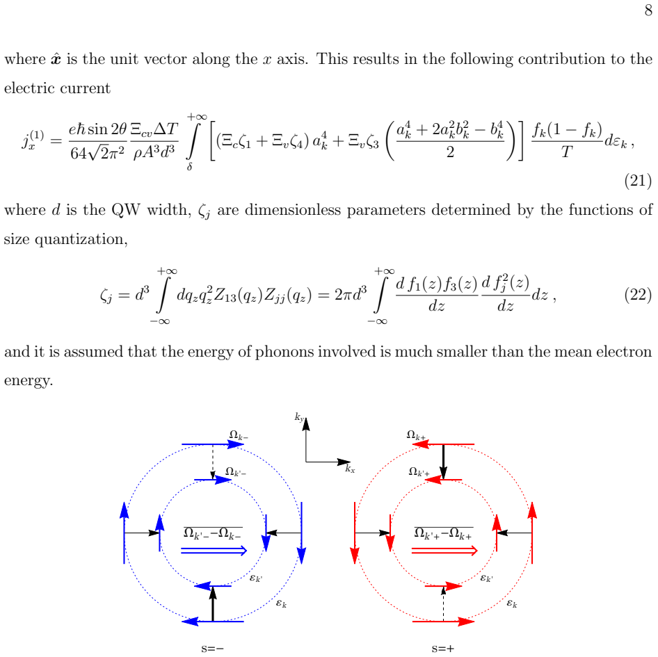
The engine of the effect is the shift vector $\mathbf{R}_{\nu'\nu} = -(\nabla_{\mathbf{k}'}+\nabla_{\mathbf{k}})\Phi_{\nu'\nu} + \boldsymbol{\Omega}_{\mathbf{k}'s'} - \boldsymbol{\Omega}_{\mathbf{k}s}$, the real-space displacement of a Bloch electron in a transition from state $\nu$ to $\nu'$. It combines a phase-gradient term and a Berry-connection term, here $\boldsymbol{\Omega}_{\mathbf{k}s} = s\, b_k^2/(2k)\, \hat{\mathbf{z}}\times\hat{\mathbf{k}}$, and only their sum is gauge invariant. The asymmetry that makes the shifts add up comes from the electron-phonon matrix elements: an interband deformation-potential term proportional to $\Xi_{cv}\sin 2\theta$ mixes the $\Gamma_6$ and $\Gamma_8$ bands, making phonon emission and absorption rates asymmetric in momentum and spin. This mechanism, combined with a Fermi-Dirac electron distribution at temperature $T_e$ and a Bose-Einstein phonon distribution at lattice temperature $T$, produces the current.
What would settle it
Grow a (013)-oriented HgTe/CdHgTe quantum well, heat its electron gas with a short THz pulse while the lattice stays at base temperature, and record the DC current along the in-plane polar axis: the formula predicts a current linear in the electron-lattice temperature difference that reverses between n-type and p-type structures and disappears for [001]- and [111]-grown wells, so an experiment seeing none of these features would refute the claim.
Extended reading notes
Core claim
The paper claims that energy relaxation of a heated two-dimensional electron gas in a non-centrosymmetric zinc-blende quantum well drives a direct electric current through a real-space shift of Bloch-electron wave packets at each phonon scattering event. The main result, Eq. (25), gives the shift current as $$j_x = \frac{e\hbar \sin 2\$\theta$ \, \Xi_{cv}\, \$\Delta$ T}{32\sqrt{2}\$pi^{2}$ \rho $A^{3}$ $d^{3}$ T} \int_\delta^\infty \left[(\Xi_c\zeta_1+\Xi_v\zeta_4)\left(2+\frac{\delta}{\varepsilon_k}\right)+\Xi_v\zeta_3\left(2-\frac{\delta}{\varepsilon_k}\right)\right] \frac{\delta}{\varepsilon_k}\, f_k(1-f_k)\, d\varepsilon_k ,$$ where the integral runs over the conduction subband and an analogous expression holds for holes. The current vanishes in equilibrium, is linear in the electron-lattice temperature difference, disappears in high-symmetry [001]- and [111]-grown wells, and changes sign between n-type and p-type structures. This is a new application of the shift mechanism previously studied in photogalvanic effects, transferred to purely thermal driving.
Load-bearing premise
The calculation assumes the hot electron gas stays internally thermalized at one effective temperature while the phonons stay at the lattice temperature, so that the emission-absorption imbalance is simply proportional to $\Delta T/T$; if phonon heating or a nonthermal electron distribution sets in, the linear current law changes.
Editorial extensions
If this is right
- A temperature imbalance alone acts as a source of DC current in (0lh)-oriented zinc-blende quantum wells, with no voltage, illumination, or magnetic field required.
- The current reverses direction when the chemical potential moves from the electron to the hole subband, so n-type and p-type structures conduct in opposite directions.
- The current is linear in $\Delta T/T$ and in $\sin 2\theta$, so it vanishes in [001]- and [111]-grown wells and can be tuned by choosing the growth orientation.
- For HgTe/CdHgTe parameters and $\Delta T = 10$ K the current is of order nA/cm; under pulsed THz or optical heating, where the energy relaxation rate is orders of magnitude larger, the current should be correspondingly larger.
- The current magnitude is proportional to the electron-lattice energy transfer rate, making the effect a direct electrical readout of how fast hot carriers cool.
Reading between the lines
- The same shift mechanism should generalize beyond zinc-blende quantum wells to any non-centrosymmetric conductor with inelastic phonon scattering, so ferroelectric thin films or wurtzite heterostructures are natural places to look.
- Cooling the electron gas below the lattice temperature should reverse the current, turning the effect into a sensitive probe of hot-carrier cooling dynamics in low-dimensional systems.
- In optical experiments on the same materials, the phonogalvanic current may coexist with the photogalvanic shift current; separating them would require comparing continuous-wave illumination with pulsed-heating conditions.
- Because $\Xi_{cv}$ enters the current linearly and the paper notes its value for HgTe is not known, a measured shift current would provide a way to determine this interband deformation-potential constant.
Signed reviews
Editorial analysis
A structured set of objections, weighed in public.
Referee Report
Summary. The manuscript proposes a phonogalvanic effect in low-symmetry zinc-blende quantum wells: a heated (or cooled) two-dimensional electron gas emits (or absorbs) acoustic phonons while relaxing toward the lattice temperature, and the accompanying real-space shift of Bloch electrons produces a direct electric current. The authors derive the shift for transitions between BHZ-type subband states, compute the deformation-potential scattering matrix elements, and obtain Eq. (25) for the shift current, together with the degenerate-limit expression Eq. (26). They argue that the current vanishes at equilibrium, is proportional to sin 2θ with the QW orientation angle, changes sign between n-type and p-type structures, and is of order nA/cm for ΔT = 10 K in HgTe/CdHgTe quantum wells.
Significance. The proposed phonogalvanic effect is conceptually interesting and connects two well-studied phenomena, energy relaxation of hot carriers and shift currents, in a way that has not, to my knowledge, been put forward before. The derivation is largely self-contained: the shift formula, the model wave functions, the deformation-potential matrix elements, and the current formula are presented in a clear sequence, and the symmetry argument for the orientation dependence sin 2θ is compelling. The explicit analytic result Eq. (25) and its sign reversal between electron and hole doping provide falsifiable predictions that could be tested in gated HgTe/CdHgTe structures. At the same time, the quantitative claim rests on an occupation-factor approximation that is not uniformly valid, as detailed below, and the numerical estimate uses an interband deformation-potential ratio borrowed from GaAs; these issues affect the magnitude but not the existence of the effect.
major comments (2)
- [Sec. III.D, Eq. (18)] The small-ΔT expansion of the emission-minus-absorption bracket in Eq. (18) is incomplete. For a transition with ε_ν' − ε_ν = ℏω_q, the exact bracket is f_ν(1−f_ν') N_q [e^{ℏω_q(β−β_e)} − 1] with β = 1/k_B T and β_e = 1/k_B T_e. For ΔT = T_e − T ≪ T this expands to f_ν(1−f_ν') N_q (ℏω_q/k_B T)(ΔT/T), or equivalently f_ν'(1−f_ν) (N_q+1)(ℏω_q/k_B T)(ΔT/T). Equation (18) omits the factor (N_q+1)ℏω_q/k_B T, which equals unity only in the equipartition limit ℏω_q ≪ k_B T. This condition is not stated in Sec. III.D, and the later comment below Eq. (22) that the phonon energy is much smaller than the mean electron energy is a different requirement. Since Eq. (18) feeds directly into Eqs. (21), (24), and (25), the predicted magnitude and the lattice-temperature dependence of the shift current are affected; the apparent absence of an explicit T dependence in Eq. (26) is an artifact of this approximation.
- [Sec. IV, Eq. (26) and Fig. 3] The numerical estimates in Fig. 3 are obtained from Eq. (26), which is derived under the same incomplete occupation-factor expansion. For HgTe/CdHgTe quantum wells with d ~ 5 nm and low lattice temperatures, the dominant phonon wave vectors have q_z ~ 1/d, giving ℏω_q/k_B T of order unity or larger, so the equipartition condition ℏω_q ≪ k_B T is likely violated in the plotted regime. The caption specifies ΔT = 10 K but does not state the lattice temperature T. The authors should either restrict the quantitative claims to the equipartition regime, carry the corrected (N_q+1)ℏω_q/k_B T factor through the k-integration, or clearly label the numbers in Fig. 3 as illustrative estimates. The existence and sign reversal of the current are likely robust, but the central quantitative claim is not established by the present calculation.
minor comments (4)
- [Sec. III.D] In the sentence after Eq. (18), 'the difference between the rates of photon emission and absorption' should read 'phonon emission and absorption'.
- [Reference [2]] The author name 'Firdkin' should be 'Fridkin' (V. M. Fridkin).
- [Sec. IV, last paragraph] The phrase 'If fact' should be 'In fact'.
- [Fig. 3 caption] The caption should state the lattice temperature T and explicitly note that the ratio Ξ_cv/Ξ_c is taken from GaAs rather than determined for HgTe.
Circularity Check
No significant circularity: Eq. (25) is a new microscopic formula; the derivation is self-contained and the self-citations are not load-bearing.
full rationale
The central result Eq. (25) is obtained by combining a standard shift formula (Eq. (5), attributed to Luttinger and to Belinicher, Ivchenko, and Sturman), a BHZ-type k·p model (Eqs. (7)-(12)), deformation-potential electron-phonon matrix elements (Eqs. (13)-(15)), and Fermi's golden rule with a quasi-equilibrium difference-of-rates approximation (Eqs. (16)-(18)). None of these inputs contains the target shift current: the temperature difference ΔT, the deformation-potential constants, and the band parameters enter as independent parameters, and no parameter is fitted to the predicted current. The authors' own earlier work is cited only for the interband deformation matrix elements [30] and for numerical k·p band parameters [32]; these are material-specific inputs, not the phonogalvanic current, so the derivation does not reduce to its own conclusion. The quasi-equilibrium approximation in Eq. (18) is a quantitative validity condition rather than a circular step, and the noted uncertainty in the ratio Ξcv/Ξc is an empirical parameter transfer from GaAs to HgTe, not a re-use of the target result. Overall, no equation or asserted prediction is identical by construction to an input or to a fitted value.
Assumptions & free parameters
free parameters (1)
- Ξcv/Ξc ratio =
1/3
assumptions (5)
- standard math The electron displacement at a quantum transition is given by Eq. (5): R = -(∇k' + ∇k)Φ + Ωk's' - Ωks, based on the wave-packet picture.
- domain assumption The 6-band k·p Hamiltonian (BHZ, Eq. 7) describes the electron and hole subbands in narrow-gap (0lh)-oriented QWs with a gap 2δ and a single parameter A; excited subbands and zero-field spin splitting are neglected.
- domain assumption The deformation-potential interaction with acoustic phonons is given by Eqs. (13)-(14), with a single Γ8 constant Ξv = a + (5/4)b and an interband constant Ξcv that couples Γ6 and Γ8 states.
- domain assumption The electron gas is internally thermalized and described by a Fermi-Dirac distribution with effective temperature Te, while phonons are at lattice temperature T, and the applied temperature difference ΔT = Te - T is small compared with T (Sec. III.D, Eq. 18).
- domain assumption Scattering of confined electrons by bulk acoustic phonons is dominated by longitudinal (LA) phonons with out-of-plane wavevector qz much larger than the in-plane component q||, and spin is conserved during scattering (Sec. III.C).
Cite this review
Pith. "Pith review of Thermal generation of shift electric current." pith.science (2026). https://pith.science/paper/EQ553KIT
@misc{pith2026190807252,
  author       = {Pith},
  title        = {Pith review of: Thermal generation of shift electric current},
  year         = {2026},
  howpublished = {\url{https://pith.science/paper/EQ553KIT}},
  note         = {Machine review of arXiv:1908.07252}
}
read the original abstract
It is shown that the dissipation of energy in an electron gas confined in a quantum well made of non-centrosymmetric crystal leads to a direct electric current. The current originates from the real-space shift of the wavepackets of Bloch electrons at the electron scattering by phonons, which tends to restore thermal equilibrium between the electron and phonon subsystems. We develop a microscopic theory of such a phonogalvanic effect for narrow band gap zinc-blende quantum wells.
Figures


Reference graph
Works this paper leans on
-
[1]
The feynman lectures on physics vol 1,
R. P. Feynman, R. B. Leighton, and M. Sands, “The feynman lectures on physics vol 1,” (San Francisco, CA: Pearson, 2006) Chap. 46
work page 2006
-
[2]
P. Sturman and V. Firdkin, Photovoltaic and Photo-refractive Effects in Noncentrosymmetric Materials, Ferroelectricity and related phenomena (Taylor & Francis, 1992)
work page 1992
-
[3]
Reimann, Physics Reports 361, 57 (2002)
P. Reimann, Physics Reports 361, 57 (2002)
2002
-
[4]
P. H¨ anggi and F. Marchesoni, Reviews of Modern Physics 81, 387 (2009)
work page 2009
-
[5]
J. Bang, R. Pan, T. M. Hoang, J. Ahn, C. Jarzynski, H. T. Quan, and T. Li, New Journal of Physics 20, 103032 (2018)
work page 2018
-
[6]
E. M. H¨ ohberger, A. Lorke, W. Wegscheider, and M. Bichler, Applied Physics Letters 78, 2905 (2001)
work page 2001
-
[7]
E. L. Ivchenko and S. D. Ganichev, JETP Letters 93, 673 (2011)
work page 2011
-
[8]
A. D. Chepelianskii, M. V. Entin, L. I. Magarill, and D. L. Shepelyansky, Physical Review E 78 (2008), 10.1103/physreve.78.041127
Show all 32 references
-
[9]
S. A. Tarasenko, Physical Review B 83 (2011), 10.1103/physrevb.83.035313
2011 doi
-
[10]
Drexler, S
C. Drexler, S. A. Tarasenko, P. Olbrich, J. Karch, M. Hirmer, F. M¨ uller, M. Gmitra, J. Fabian, 13 R. Yakimova, S. Lara-Avila, S. Kubatkin, M. Wang, R. Vajtai, P. M. Ajayan, J. Kono, and S. D. Ganichev, Nature Nanotechnology 8, 104 (2013)
2013
-
[11]
G. V. Budkin and S. A. Tarasenko, Phys. Rev. B 93, 075306 (2016)
2016
-
[12]
S. D. Ganichev, E. L. Ivchenko, V. V. Bel’kov, S. A. Tarasenko, M. Sollinger, D. Weiss, W. Wegscheider, and W. Prettl, Nature 417, 153 (2002)
2002
-
[13]
Seibold, S
G. Seibold, S. Caprara, M. Grilli, and R. Raimondi, Physical Review Letters 119 (2017), 10.1103/physrevlett.119.256801
2017 doi
-
[14]
Smirnov and L
D. Smirnov and L. Golub, Physical Review Letters 118 (2017), 10.1103/phys- revlett.118.116801
2017 doi
-
[15]
J. M. Luttinger, Physical Review 112, 739 (1958)
1958
-
[16]
N. A. Sinitsyn, Journal of Physics: Condensed Matter 20, 023201 (2007)
2007
-
[17]
Nagaosa, J
N. Nagaosa, J. Sinova, S. Onoda, A. H. MacDonald, and N. P. Ong, Rev. Mod. Phys. 82, 1539 (2010)
2010
-
[18]
L. N. Oveshnikov, V. A. Kulbachinskii, A. B. Davydov, B. A. Aronzon, I. V. Rozhansky, N. S. Averkiev, K. I. Kugel, and V. Tripathi, Scientific Reports 5 (2015), 10.1038/srep17158
2015 doi
-
[19]
I. A. Ado, I. A. Dmitriev, P. M. Ostrovsky, and M. Titov, Phys. Rev. B 96, 235148 (2017)
2017
-
[20]
C. Xiao, Y. Liu, M. Xie, S. A. Yang, and Q. Niu, Phys. Rev. B 99, 245418 (2019)
2019
-
[21]
V. I. Belinicher, E. L. Ivchenko, and B. I. Sturman, Sov. Phys. JETP 56, 359 (1982)
1982
-
[22]
L. E. Golub and E. L. Ivchenko, JETP 112, 152 (2011)
2011
-
[23]
E. M. Baskin, L. I. Magarill, and M. V. Entin, Fizika Tverdogo Tela 20, 2432 (1978)
1978
-
[24]
B. A. Bernevig, T. L. Hughes, and S.-C. Zhang, Science 314, 1757 (2006)
2006
-
[25]
Winkler, L
R. Winkler, L. Wang, Y. Lin, and C. Chu, Solid State Communications 152, 2096 (2012)
2012
-
[26]
S. A. Tarasenko, M. V. Durnev, M. O. Nestoklon, E. L. Ivchenko, J.-W. Luo, and A. Zunger, Phys. Rev. B 91, 081302 (2015)
2015
-
[27]
Gantmakher and I
V. Gantmakher and I. Levinson, Carrier scattering in metals and semiconductors , Modern problems in condensed matter sciences (North-Holland, 1987)
1987
-
[28]
Bir and G
G. Bir and G. Pikus, Symmetry and Strain-induced Effects in Semiconductors , A Halsted Press book (Wiley, 1974)
1974
-
[29]
G. E. Pikus, V. A. Marushchak, and A. N. Titkov, Sov. Phys. Semicond. 22, 115 (1988)
1988
-
[30]
Olbrich, C
P. Olbrich, C. Zoth, P. Vierling, K.-M. Dantscher, G. V. Budkin, S. A. Tarasenko, V. V. Bel’kov, D. A. Kozlov, Z. D. Kvon, N. N. Mikhailov, S. A. Dvoretsky, and S. D. Ganichev, 14 Phys. Rev. B 87, 235439 (2013)
2013
-
[31]
Adachi, Handbook on Physical Properties of Semiconductors
S. Adachi, Handbook on Physical Properties of Semiconductors. Volume 3: II—VI Compound Semiconductorst (Kluwer Academic Publishers, 2004)
2004
-
[32]
Dantscher, D
K.-M. Dantscher, D. A. Kozlov, P. Olbrich, C. Zoth, P. Faltermeier, M. Lindner, G. V. Budkin, S. A. Tarasenko, V. V. Bel’kov, Z. D. Kvon, N. N. Mikhailov, S. A. Dvoretsky, D. Weiss, B. Jenichen, and S. D. Ganichev, Phys. Rev. B 92, 165314 (2015)
2015
Reviewed August 14, 2026 · model on record in the stance chip above.
Discussion (0). Continue with ORCID to comment.