REVIEW 2 major objections 4 minor 26 references
Nano-Fabricated Free-Standing Wire-Scanners with Sub-Micrometer Resolution
T0 review · 2 major / 4 minor · reviewed 2026-08-14 · deepseek-v4-flash
Pith's one-line read Nano stripes give wire scanners 250-nm resolution.
desk verdict A credible first demonstration of free-standing sub-micrometer wire scanners for electron beams; the missing encoder/vibration calibration is a moderate, fixable weakness. read the letter →
The pith
A machine-rendered reading of the paper's core claim, the machinery that carries it, and where it could break.
The reading
What carries the argument
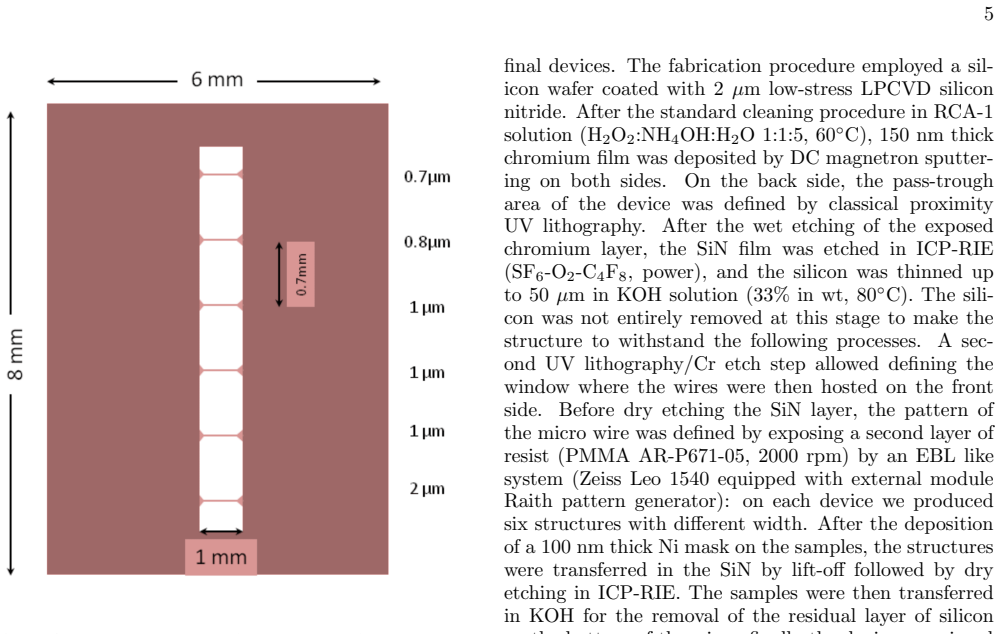
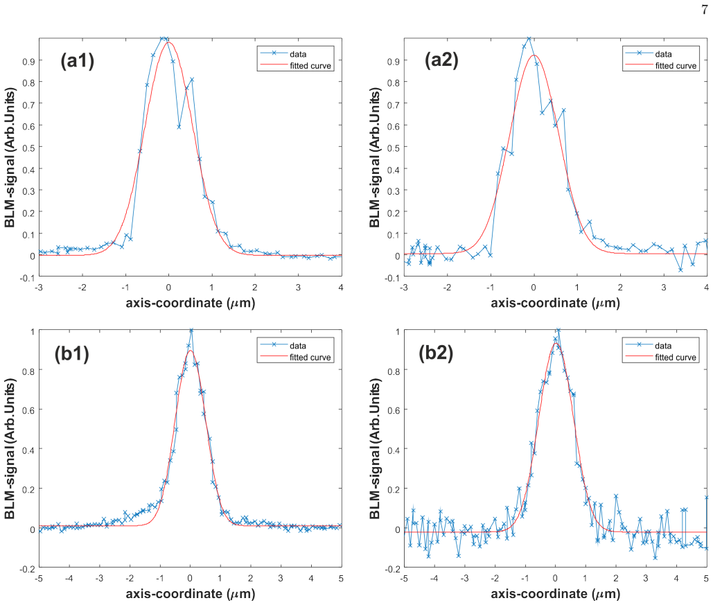
The central object is the free-standing nano-fabricated stripe, a lithographically defined rectangular beam probe suspended across a window in a silicon frame, replacing the drawn metallic wire of a conventional scanner. Its nominal geometric resolution is the rms width of a rectangular distribution, $\sigma_{\rm rms} = w/\sqrt{12}$, which is about 250 nm for the tested 800–900 nm stripes; the measured profile is reconstructed by correlating the encoder-reported stripe position with the signal of a beam-loss monitor about 2 m downstream. The analysis separates beam size from stripe width by fitting the data to a Gaussian distribution convolved with a rectangle, expressed through error functions in Eq. (1), with the stripe width $w$ fixed. This separation is what allows the authors to claim that a measured 400–500 nm vertical beam size is real rather than a convolution artifact.
What would settle it
Scan a beam whose size is known independently—for example by a quadrupole-scan emittance measurement or by a second stripe much narrower than 800 nm—and compare the fitted vertical size: if the fitted size grows with stripe width, unaccounted encoder error or wire vibration is inflating the reported 400–500 nm values. The same check could be made directly by measuring stripe vibration with an optical vibrometer during a scan and looking for amplitudes comparable to 250 nm.
Extended reading notes
Core claim
On the paper's own terms, the discovery is that a free-standing sub-micrometer wire scanner is not just fabricable but operational: a 900 nm wide, 2 mm long bulk-gold stripe and an 800 nm wide, 0.8 mm long Au/Si3N4/Au sandwich stripe, each nano-fabricated directly onto a silicon frame, reach geometric resolutions of 260 nm and 230 nm respectively (stripe width divided by $\sqrt{12}$). In low-charge, low-emittance runs at 300 MeV with a vertical emittance near 55 nm and $\beta$ function $\beta_y = 2.61\times 10^{-3}$ m, the expected vertical beam size was about 480 nm, and both stripes fitted the measured profiles—using the error-function convolution of Eq. (1)—to vertical sizes of $488\pm20$ nm and $477\pm70$ nm in one session and $434\pm7$ nm and $443\pm33$ nm in another. The same devices were then scanned repeatedly at 200 pC bunch charge without observable heat damage. The conclusion the authors draw is that nano-fabricated free-standing stripes extend wire-scanner diagnostics into the sub-micrometer regime while reducing the surface of impact on the beam, and that the remaining step for routine FEL use is increasing the 2 mm beam clearance by a factor of 4–5.
Load-bearing premise
The measurement assumes that the stripe position reported by the encoder matches the stripe's position in the beam to far better than 250 nm, with wire vibrations and positioning errors negligible at that scale.
Editorial extensions
If this is right
- Wire-scanner resolution in FELs can be improved from the micrometer scale to a few hundred nanometers, limited mainly by the stripe width.
- The smaller impact surface reduces beam losses and the energy and angular spread imparted to scanned electrons, improving transparency to lasing.
- Both fabrication routes—bulk gold and Au/Si3N4/Au sandwich—yield working devices, so the choice of stripe material can be traded between signal-to-noise and radiation length.
- Nominal-charge heat loading at 200 pC did not damage either stripe, supporting use during routine machine operation.
- For routine deployment the 2 mm beam clearance must be enlarged by a factor of 4–5, as the paper states.
Reading between the lines
- If encoder positioning and stripe vibration are indeed negligible at the 250 nm scale, the same devices could resolve even smaller beams by narrowing the stripe further; the practical limit would shift from fabrication to mechanical stability and readout precision.
- The paper does not quantify encoder accuracy or vibration, but a straightforward extension would be to scan a beam of known size through a focus waist and compare the stripe result with an independent emittance or optical-diffraction measurement.
- Because the stripes are produced by standard lithography on a chip, arrays of different widths on one holder could serve as self-calibrating diagnostics, checking resolution by comparing fits at different stripe widths.
Signed reviews
Editorial analysis
A structured set of objections, weighed in public.
Referee Report
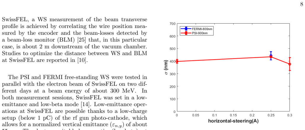
Summary. The paper reports the fabrication and beam-test results of free-standing nano-fabricated wire scanners (WS) developed independently at PSI and FERMI. The devices consist of sub-micrometer-wide gold (PSI) or Au/Si3N4/Au sandwich (FERMI) stripes, 900 nm and 800 nm wide respectively, with a nominal geometric resolution of about 250 nm (w/sqrt(12)). The scanners were tested at SwissFEL in low-charge, low-emittance mode, where they measured vertical beam sizes of 400-500 nm, consistent with the expected size from emittance and beta function, and they were also exposed to 200 pC beams to test heat-loading resilience. The data analysis uses an error-function convolution fit, Eq. (1), that deconvolves the rectangular stripe response. The paper also presents a horizontal-steering reproducibility test and comparative signal-to-noise observations for the two scanner types.
Significance. If the results hold, this work demonstrates a practical route to extending wire-scanner diagnostics from the micrometer into the sub-micrometer regime, which is directly relevant to low-emittance FEL operation and to plasma- and laser-driven accelerator beam diagnostics. The strength of the paper is its dual independent fabrication routes and the cross-checked experimental campaign: two facilities, two measurement sessions, consistency with the emittance-based expectation, and a horizontal-steering reproducibility test. The analysis formula is standard and the fit parameters are outputs, not forced inputs, so there is no circularity concern. The main weakness is that the measurement accuracy of the wire position relative to the beam is not quantified, which is critical for the central resolution claim.
major comments (2)
- [Sec. IV, Eq. (1), Table I] The central measurement claim requires that the encoder readout accurately represents the vertical position of the free-standing stripe during the scan, but the manuscript never quantifies the encoder resolution or accuracy, the mechanical repeatability/backlash of the sample holder, or possible vibration of the 2 mm (PSI) and 0.8 mm (FERMI) free-standing stripes. Section I itself lists "measurement resolution of the wire positioning" and "possible wire vibrations" as components of the spatial resolution, yet neither is bounded in Section IV. Since Eq. (1) deconvolves only the known rectangular width w, any additional position jitter or scale error is absorbed into the fitted sigma; with fitted sigmas of 434-488 nm and a geometric term of 230-260 nm, an unquantified position uncertainty of 50-100 nm is not negligible. The horizontal-steering test in Fig. 7 checks reproducibility versus horizontal beam position but does not validate the vertical position scale. I request an explicit uncertainty budget for the encoder-to-stripe coordinate link, or a demonstration that its contribution is small compared with w/sqrt(12).
- [Sec. IV, heat-loading test] The heat-loading resilience claim ("No damage ... after several and repeated series of measurements at a beam charge of 200 pC") is purely qualitative: no inspection criterion is defined, no number of scans or accumulated charge is reported, and no before/after comparison of the stripe integrity is shown. Since resilience at nominal charge is part of the abstract's central claim, the authors should either quantify the test (number of shots, total dose, SEM verification) or soften the claim to "no damage observed in a limited test."
minor comments (4)
- [Header] The line "PACS numbers:" is left empty; either provide PACS codes or remove the line.
- [Table I and Sec. IV] The column "beam size" is not explicitly labeled as the rms beam size σ; please state this in the table caption or text to avoid confusion with peak-to-peak values.
- [Eq. (1)] The stripe width w is treated as a known constant without a tolerance; although a ±50 nm width uncertainty would change the deconvolved σ by only about 14 nm, stating the measured width and its uncertainty would improve the rigor of the deconvolution.
- [Sec. IV] The sentence "The FERMI WS stripe being a sandwich structure ... is characterized by a radiation length about two times longer than the PSI WS" should clarify whether the effective radiation length per unit thickness or the total energy loss is meant, since the two are different for a multilayer structure.
Circularity Check
No circularity found: the central result is an experimental measurement, and the only formulas used are standard definitions or fits whose free parameters are outputs.
full rationale
The paper's load-bearing claims are the fabrication of 900/800 nm free-standing stripes and the SwissFEL measurements of a 400–500 nm vertical beam size. The geometric resolution w/sqrt(12) is a standard definition supplied in Eq. (A3), not a derived prediction. The expected beam size is computed independently from the machine optics (beta_y = 2.61e-3 m, normalized emittance 55 nm, gamma at 300 MeV), and the measured size is obtained by fitting Eq. (1) with w predefined from the stripe width and a, b, c, sigma free; no fitted input is renamed as a prediction. The self-citations (Refs. 10, 14, 15, 19, 20, 24) are experimental antecedents or hardware descriptions, and none is used to forbid alternatives or to supply the uniqueness of the measured beam size. The unquantified encoder accuracy and possible stripe vibration are experimental limitations that could bias the measurements, but they are not circular reductions of the derivation; the paper's analysis does not define the measured quantity in terms of itself.
Assumptions & free parameters
assumptions (5)
- domain assumption The electron beam transverse profile is well approximated by a Gaussian distribution with standard deviation sigma.
- standard math The rms geometric resolution of a rectangular wire of width w is w/sqrt(12).
- domain assumption The vertical beam size at the interaction point is sigma_y = sqrt(beta_y * epsilon_n,y / gamma).
- standard math The energy radiated by an ultrarelativistic electron crossing material is dE/E = dX/L_R.
- domain assumption The wire position as read by the encoder corresponds to the actual position of the stripe in the beam, with negligible vibration.
Cite this review
Pith. "Pith review of Nano-Fabricated Free-Standing Wire-Scanners with Sub-Micrometer Resolution." pith.science (2026). https://pith.science/paper/2UFBVEGJ
@misc{pith2026190807468,
  author       = {Pith},
  title        = {Pith review of: Nano-Fabricated Free-Standing Wire-Scanners with Sub-Micrometer Resolution},
  year         = {2026},
  howpublished = {\url{https://pith.science/paper/2UFBVEGJ}},
  note         = {Machine review of arXiv:1908.07468}
}
read the original abstract
Diagnostics of the beam transverse profile with ever more demanding spatial resolution is required by the progress on novel particle accelerators - such as laser and plasma driven accelerators - and by the stringent beam specifications of the new generation of X-ray facilities. In a linac driven Free-Electron-Laser (FEL), the spatial resolution constraint joins with the further requirement for the diagnostics to be minimally invasive in order to protect radiation sensitive components - such as the undulators - and to preserve the lasing mechanism. As for high resolution measurements of the beam transverse profile in a FEL, wire-scanners (WS) are the top-ranked diagnostics. Nevertheless, conventional WS consisting of a metallic wire (beam-probe) stretched onto a frame (fork) can provide at best a rms spatial resolution at the micrometer scale along with an equivalent surface of impact on the electron beam. In order to improve the spatial resolution of a WS beyond the micrometer scale along with the transparency to the lasing, PSI and FERMI are independently pursuing the technique of the nano-lithography to fabricate a free-standing and sub-micrometer wide WS beam-probe fully integrated into a fork. Free-standing WS with a geometrical resolution of about 250 nm have been successfully tested at SwissFEL where low charge electron beams with a vertical size of 400-500 nm have been characterized. Further experimental tests carried out at SwissFEL at the nominal beam charge of 200 pC confirmed the resilience to the heat-loading of the nano-fabricated WS. In this work, details on the nano-fabrication of free-standing WS as well as results of the electron-beam characterization are presented.
Figures


Figures from the paper (4 more)


Reference graph
Works this paper leans on
- [1]
-
[2]
M.C. Ross, J. T. Seeman, E. Bong, L. Hendrickson, D. McCormick, L. Sanchez-Chopitea, Particle Accelerator Conference (PAC) 1991
work page 1991
- [3]
-
[4]
P. Tenenbaum and T. Shintake, Annu. Rev. Nucl. Part. Sci. 1999. 49:12562
work page 1999
- [5]
-
[6]
H. Loos, R. Akre, A. Brachmann, R. Coffee, F.-J. Decker, Y. Ding, D. Dowell, S. Edstrom, P. Emma, A. Fisher, J. Frisch, S. Gilevich, G. Hays, Ph. Hering, Z. Huang, R. Iverson, M. Messerschmidt, A. Miahnahri, S. Moeller, H.-D. Nuhn, D. Ratner, J. Rzepiela, T. Smith, P. Stefan, H. Tompkins, J. Turner, J. Welch, W. White, J. Wu, G. Yocky, Operational Performa...
-
[7]
J. Wu, P. Emma, and R.C. Field Electron Signal De- tection for the Beam-Finder Wire of the Linac Coher- ent Light Source Undulator , SLAC-PUB-12120 LCLS- TN-06-7, April 2006
work page 2006
- [8]
Show all 26 references
-
[9]
Hahn, N.v
U. Hahn, N.v. Bargen, P. Castro, O. Hensler, S. Karstensen, M. Sachwitz, H. Thom, Nuclear Instruments and Methods in Physics Research A 592 (2008) 189196
2008
-
[10]
Orlandi, P
G.L. Orlandi, P. Heimgartner, R. Ischebeck, C. Ozkan Loch, S. Trovati, P. Valitutti, V. Schlott, M. Ferianis, G. Penco, Design and experimental tests of free electron laser wire scanners , Phys. Rev. Accel. Beams 19, 092802 (2016)
2016
-
[11]
Huang, H
Y.C. Huang, H. Wang, R.H. Pantell, J.F. Schmerge, J.W. Lewellen, J. Feinstein, Electron Beam Characterization for a Compact Far-Infrared Free-Electron-Laser , IEEE Journal of Quantum Electronics,31, 9, (1995) 1637-1641
1995
-
[12]
They were experimentally tested at SwissFEL both in the nominal- and low-charge regime (bunch charge of 200 pC and below 1 pC, respectively)
of about 250 nm (see [23] for the formal definition of the rms geometric resolution in the case of a rectangular wire). They were experimentally tested at SwissFEL both in the nominal- and low-charge regime (bunch charge of 200 pC and below 1 pC, respectively). The electron bea...
2000
-
[13]
Veronese, A
M. Veronese, A. Abrami, E. Allaria, T. Borden, M. Bossi, A. Bucconi, F. Cianciosi, M. De Marco, M. Ferianis, L. Fr¨ ohlich, L. Giannessi, S. Grulja, R. Sauro, C. Spezzani, M. Tudor, Intra undulator screen diagnostic for the FERMI@Elettra FEL , Pro- ceedings of IBIC2012, Tsukub...
2012
-
[14]
Ischebeck, E
R. Ischebeck, E. Prat, V. Thominet, C. Ozkan Loch, Phys. Rev. ST Accel. Beams 18, 082802 (2015)
2015
-
[15]
Borrelli, G.L
S. Borrelli, G.L. Orlandi, M. Bednarzik, C. David, E. Ferrari, V. A. Guzenko, C. Ozkan-Loch, E. Prat, R Ischebeck, Generation and Measurement of Sub- Micrometer Relativistic Electron Beams , Communica- tions Physics-Nature, 1, 52 (2018)
2018
-
[16]
Veronese, S
M. Veronese, S. Grulja, G. Penco, M. Ferianis, L. Fr¨ ohlich, S. Dal Zilio, S. Greco, M. Lazzarino,A nanofab- ricated wirescanner with free standing wires: Design, fab- rication and experimental results , Nuclear Instruments and Methods in Physics Research Section A: Acceler- ...
2018
-
[17]
10-04 April 2012
SwissFEL Conceptual Design Report, PSI Bericht Nr. 10-04 April 2012
2012
-
[18]
Schietinger, et al., Commissioning experience and beam physics measurements at the SwissFEL Injector Test Facility, Physical Review Accelerators and Beams 19, 100702 (2016)
T. Schietinger, et al., Commissioning experience and beam physics measurements at the SwissFEL Injector Test Facility, Physical Review Accelerators and Beams 19, 100702 (2016)
2016
-
[19]
Milne, et al., SwissFEL: The Swiss X-ray Free Elec- tron Laser, Appl
C.J. Milne, et al., SwissFEL: The Swiss X-ray Free Elec- tron Laser, Appl. Sci. 2017, 7(7), 720
2017
-
[20]
Orlandi, A
G.L. Orlandi, A. Alarcon, S. Borrelli, A. Gobbo, P. Heimgartner, R. Ischebeck, D. Llorente, F. L¨ ohl, C. Ozkan Loch, P. Pollet, B. Rippstein, V. Schlott, R. Vintar First Experimental Results of the Commis- sioning of the SwissFEL wire-scanners , Proceedings of IBIC2017 Confer...
2017
-
[21]
E. Prat, P. Dijkstal, M. Aiba, S. Bettoni, P. Craievich, E. Ferrari, R. Ischebeck, F. L¨ ohl, A. Malyzhenkov, G.L. Orlandi, S. Reiche, and T. Schietinger, Measurements of ultra-low emittance electron-beams for compact X-ray free-electron-lasers, to be submitted for publication
-
[22]
Jurani´ c, J
P. Jurani´ c, J. Rehanek, C. A. Arrell, C. Pradervand, R. Ischebeck, C. Erny, P. Heimgartner, I. Gorgisyan, V. Thominet, K. Tiedtke, A. Sorokin, R. Follath, M. Makita, G. Seniutinas, C. David, C. J. Milne, H. Lemke, M. Radovic, C. P. Hauri and L. Patthey, SwissFEL Aramis beaml...
2018
-
[23]
Fernow, Introduction to Experimental Particle Physics, Cambridge University Press (1986)
R.C. Fernow, Introduction to Experimental Particle Physics, Cambridge University Press (1986)
1986
-
[24]
For a rectangular stripe having a 1-dimensional normal- ized spatial distribution ( −w/2,w/ 2), the square of the rms geometric resolution reads: σ2 rms = (1/w) ∫ w/2 −w/2 x2dx =w2/12 (A3)
-
[25]
Ferrari, R
E. Ferrari, R. Ischebeck, M. Bednarzik, S. Bettoni, S. Borrelli, H.-H. Braun, M. Calvi, C. David, M. Dehler, F. Frei, T. Garvey, V.A. Guzenko, N. Hiller, P. Hom- melhoff, J. McNeur, G.L. Orlandi, C. Ozkan-Loch, E. Prat, S. Reiche, A. Romann, B. Sarafinov, L. Rivkin, The ACHIP ex...
2018
-
[26]
Ozkan Loch, D
C. Ozkan Loch, D. Llorente Sancho, P. Pollet, G. Marinkovic, R. Ischebeck, V. Schlott, Proceedings of IBIC2015, Melbourne, Australia, September 2015 (MOPB051)
2015
Reviewed August 14, 2026 · model on record in the stance chip above.
Discussion (0). Continue with ORCID to comment.