REVIEW 4 major objections 4 minor 33 references
Molecular characterization of macroscopic aerogels of single-walled carbon nanotubes
T0 review · 4 major / 4 minor · reviewed 2026-08-14 · deepseek-v4-flash
Pith's one-line read This paper finds that FCCVD-grown SWCNT fibers contain a mix of semiconducting and metallic nanotubes, and that the semiconducting fraction becomes visible when the aerogel is examined before densification.
desk verdict A genuinely useful observation about semiconducting tubes being masked in densified SWCNT fibers, wrapped in an overclaimed (n,m) distribution that the limited Raman data cannot fully support. read the letter →
The pith
A machine-rendered reading of the paper's core claim, the machinery that carries it, and where it could break.
The reading
What carries the argument
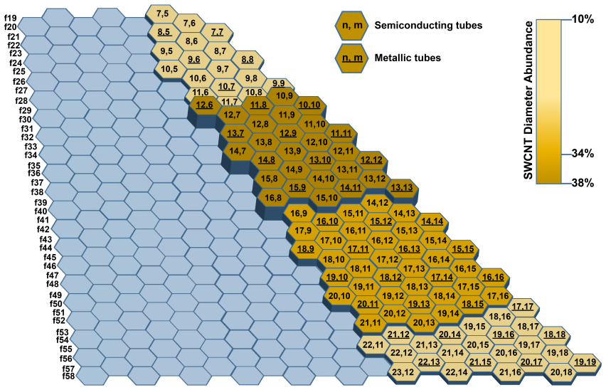
The key machinery is the open aerogel network, which leaves bundles separated by 1.5 to 2 µm, larger than the roughly 1 µm Raman laser spot, so each spectrum can come from an individual bundle. The G- lineshape (Lorentzian versus Breit-Wigner-Fano) then tags each bundle's metallicity, anchoring the radial breathing mode peaks onto the Kataura plot for family assignment within a ±50 meV resonance window.
What would settle it
Measure the same aerogel with a tunable laser spanning the S33 and S44 transition energies of 1.5–2 nm tubes; if the resulting family assignments differ from those reported with the fixed 532, 633, and 785 nm lines, the reported distribution is wrong. A simpler check: pick a bundle whose G- band is purely Lorentzian (semiconducting) and obtain its electron diffraction pattern; if the pattern indexes to a metallic (n,m), the G- lineshape criterion fails.
Extended reading notes
Core claim
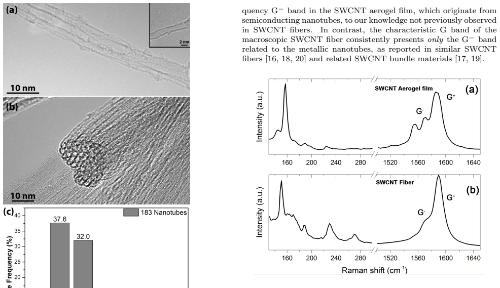
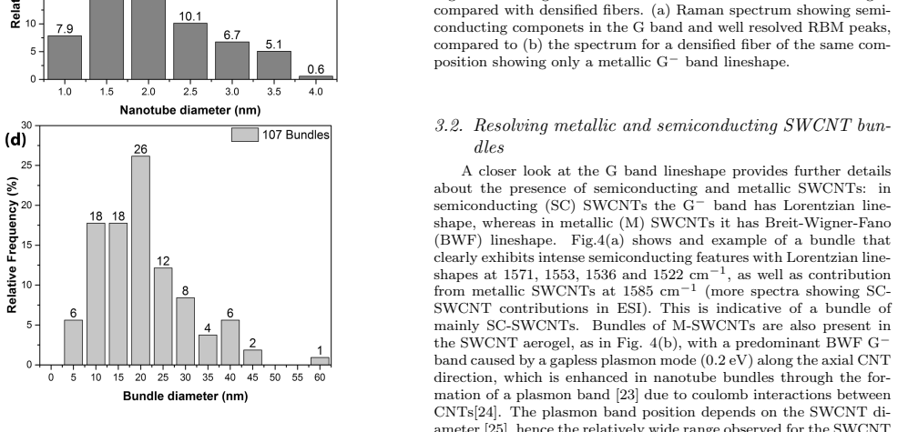
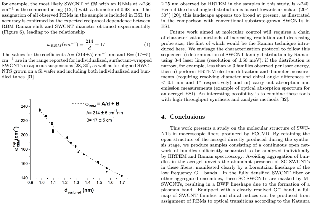
The central discovery is that the apparent metallicity of FCCVD-grown SWCNT fibers is an artifact of bundling: the dense fiber shows only a metallic Breit-Wigner-Fano G- band, but the same material in its open aerogel state shows well-resolved Lorentzian G- components from semiconducting nanotubes. Approximately 20% of the bundles probed show semiconducting features, and the RBM peaks from individual bundles can be assigned to (n,m) families grouped by optical transitions, yielding a full family distribution consistent with HRTEM diameter measurements and electron diffraction chiral angles. The empirical relation ω_RBM = 214/d + 17 cm⁻¹ confirms the assignment consistency, with coefficients in the range reported for surfactant-wrapped and aligned SWCNTs.
Load-bearing premise
The assignment of (n,m) families relies on the Kataura plot with a fixed ±50 meV resonance window, but for the largest and most abundant tubes (1.5–2 nm) the relevant third- and fourth-order optical transitions are expected to deviate from that plot, so the family distribution is uncertain precisely where it matters most.
Editorial extensions
If this is right
- Densified SWCNT fibers from FCCVD contain a substantial semiconducting population that standard Raman measurements miss, so conductivity models for these fibers must account for the true metallicity mix.
- The aerogel protocol gives a rapid, large-area screen for chiral family distributions, replacing slow statistical electron diffraction for routine fiber optimization.
- The empirical RBM–diameter relation ω_RBM = 214/d + 17 holds for bundled aerogel SWCNTs, matching surfactant-wrapped and aligned samples, so family assignment is on firm ground.
- The observed family distribution overlapping the electron-diffraction chiral angle distribution means Raman and diffraction now agree on the molecular structure of these fibers.
- Future synthesis of narrower-diameter SWCNTs would reduce the ~240 possible chiral indices, and the Raman screen would be able to detect such narrowing.
Reading between the lines
- If the aerogel reveals the true semiconducting fraction, then prior Raman studies reporting 'metallic' fibers from FCCVD may have systematically misread the metallicity; other aggregated CNT materials (films, yarns) examined by Raman alone could harbor similarly hidden semiconductor populations.
- The acknowledged S33/S44 deviation from the Kataura plot for 1.5–2 nm tubes suggests that a tunable-laser Raman sweep would refine or correct the (n,m) assignments; the paper's reported family distribution is best read as provisional until such a sweep is done.
- The open aerogel format could be paired with four-probe transport or Kelvin probe measurements on the same individual bundles, linking the G- lineshape classification to bundle-level conductivity and testing whether semiconducting bundles indeed conduct poorly.
- A testable extension: measuring the same aerogel with a tunable laser across the S33/S44 range would either confirm the reported families or shift them, and the corrected distribution could then be compared against the electron diffraction map to quantify how much of the assignment uncertainty matters.
Signed reviews
Editorial analysis
A structured set of objections, weighed in public.
Referee Report
Summary. This manuscript reports a Raman spectroscopy and HRTEM study of SWCNT aerogels produced by the floating-catalyst CVD direct spinning method. The key observation is that, by retaining the open aerogel network rather than densifying it into a fiber, the authors resolve semiconducting SWCNT features—particularly Lorentzian G− components and well-resolved RBM peaks—that are masked in the densified fiber. From RBM assignments using a Kataura-plot approach, the authors claim a full distribution of (n,m) families and a relative metallic-to-semiconducting ratio, and they compare this distribution with TEM diameter statistics and prior electron diffraction chiral-angle data. They also discuss the role of bundling in the G-band lineshape and propose the aerogel format as a rapid molecular screening tool.
Significance. If the central qualitative claim holds, the paper is significant: it demonstrates that semiconducting SWCNTs are present in FCCVD fibers but are spectroscopically hidden in the aggregated fiber, and it offers a practical sample format for Raman-based screening of molecular features in macroscopic CNT assemblies. The strength of the work is the direct aerogel-versus-fiber comparison on chemically identical material, the support from HRTEM diameter distributions over 100+ images, and the explicit acknowledgment of assignment challenges. However, the quantitative claims of a full family distribution and a metallic-to-semiconducting ratio are not supported at the same level as the qualitative presence claim, and the paper would need to either temper those claims or provide additional validation.
major comments (4)
- [§3.3, Fig. 5] The full (n,m) family distribution rests on assigning RBM peaks to transitions within a fixed ±50 meV window on a standard Kataura plot. For the dominant diameters of 1.5–2 nm, the relevant transitions are S33/S44 and higher-order metallic transitions, which the authors themselves note (citing Araujo et al.) are more likely to deviate from the single-particle Kataura energies. With only three fixed laser lines, multiple candidate (n,m) tubes will fall inside the resonance window, so the derived family distribution is underdetermined. I request a sensitivity analysis: for each assigned RBM peak, report how many (n,m) candidates fall within the window and whether the assignments survive plausible shifts of the transition energies; alternatively, state explicitly that the family distribution is tentative for these diameters.
- [§3.3, Eq. (1) and Fig. 6] The RBM frequency–diameter relation ω_RBM = 214/d + 17 is fitted from diameters that were themselves inferred from the Kataura assignments, and this same relation is then presented as confirmation of those assignments. This is a circular consistency check rather than an independent validation. The agreement with literature coefficients is suggestive, but it cannot break degeneracies among candidate (n,m) assignments. Please rephrase the claim so that Eq. (1) is presented as an internal consistency check, or provide independent diameter measurements (e.g., from TEM statistics constrained to the same tubes) to support the assignments.
- [§3.2, Fig. 4(c)] The introduction promises a 'relative ratio of metallic to semiconducting tubes', but the operationalized result in §3.2 is that 'semiconducting SWCNTs are present in 20% of the bundles probed' based on about 30 spectra. This is a bundle-level count with a small sample, not a tube-level ratio. The text should be corrected to state what was actually measured, and the statistical uncertainty of the 20% fraction should be given; otherwise the M/S ratio claim is misleading.
- [Fig. 7 and Conclusions] The agreement between the Raman-derived families and the HRTEM/electron-diffraction distribution is presented as a validation of a 'full map' or 'full distribution'. However, the Raman data only cover families accessible with three laser lines and the comparison in Fig. 7 is qualitative, using the authors' own prior electron diffraction results. The claim of a full distribution should be softened to 'a partial family distribution consistent with TEM/ED data' unless all families expected from the diameter distribution are actually observed or a quantitative overlap metric is provided.
minor comments (4)
- [§2.2] There are several typos: 'not that all spectra' should read 'note that all spectra', 'waveleght' should be 'wavelength', and 'electon diffraction' should be 'electron diffraction'.
- [Fig. 2(c-d)] The histograms for SWCNT and bundle diameters should state whether they are number-weighted or length-weighted, and the number of measured nanotubes and bundles used for each histogram should be given in the caption.
- [§3.1] The D/G ratio of 0.06 ± 0.02 is reported without the number of spectra or the standard deviation source; please specify the statistics and the laser wavelength used for this value.
- [§3.3] The procedure of Maultzsch et al. is cited, but the paper should explicitly state which environment corrections (e.g., Van der Waals downshifts) were applied and what parameter values were used for the Kataura plot, since the resonance window of ±50 meV is one of the free parameters of the method.
Circularity Check
RBM-diameter fit is used to confirm its own input assignments; the central semiconducting/metallic presence claim remains independently supported.
-
fitted input called prediction
[Section 3.3 (SWCNT assignation), Eq. (1) and Fig. 6]
"Its accuracy is confirmed by the expected reciprocal dependence between RBM Raman shift and SWCNT diameter obtained experimentally (Figure 6), leading to the relationship ωRBM (cm−1) = 214/d + 17 (1). The values for the coefficients A= (214±5) cm−1·nm and B= (17±5) cm−1 are in the range reported for individualized, surfactant-wrapped SWCNTs in aqueous suspensions [28,30]."
The diameters used to fit Eq. (1) come from the same (n,m) assignments whose accuracy Eq. (1) is then said to confirm. In the assignment step, observed RBM frequencies are placed on the Kataura plot and matched to family branches and ±50 meV resonances; the 'corresponding assigned nanotube diameter' in Fig. 6 is therefore derived from the RBM peaks and Kataura assignments, not measured independently. Fitting ω_RBM = A/d + B to those derived diameters and presenting the resulting reciprocal dependence as confirmation of the assignments is a self-consistency check, not an independent test; any internally consistent mapping of the assigned diameters would reproduce the input relation.
full rationale
The paper's principal qualitative claim—that semiconducting and metallic SWCNTs are both present in the open aerogel and that semiconducting features are masked in densified fibers—is supported by the Lorentzian versus Breit-Wigner-Fano G− line-shape comparison in Section 3.2, which does not depend on (n,m) assignment. The identified circular step is confined to the validation of the (n,m) assignments via Eq. (1): the fitted RBM-frequency-versus-diameter relation is derived from diameters assigned through the very RBM/Kataura procedure it is then used to confirm, so it is a consistency check rather than independent evidence. The comparison in Figure 7 with the chiral angle distribution from Ref. [20] is a self-citation, but it uses electron diffraction data from an independent measurement technique and is therefore not circular. The acknowledged difficulty of assigning S33/S44 transitions for the dominant 1.5–2 nm diameters is a real uncertainty in the quantitative family distribution, but it is a correctness risk rather than a circularity. Taking these together, the central presence claim stands independently while the quantitative distribution claim is only partially anchored by an independent check, giving a moderate score of 4.
Assumptions & free parameters
free parameters (3)
- A coefficient in RBM diameter relation =
214 ± 5 cm^-1·nm
- B coefficient in RBM diameter relation =
17 ± 5 cm^-1
- Resonance energy window =
±50 meV
assumptions (4)
- domain assumption Kataura plot relation between optical transition energies, diameter, and chiral family, with environmental downshifts as per Maultzsch et al. [28].
- domain assumption Lorentzian G^- lineshape indicates semiconducting tubes and BWF lineshape indicates metallic tubes.
- domain assumption The aerogel sample is chemically identical to the densified fiber, so observations on the aerogel represent the fiber's molecular composition.
- domain assumption RBM frequency is inversely proportional to diameter with constant coefficients (Eq. 1).
Cite this review
Pith. "Pith review of Molecular characterization of macroscopic aerogels of single-walled carbon nanotubes." pith.science (2026). https://pith.science/paper/7VMN3CN3
@misc{pith2026190808230,
  author       = {Pith},
  title        = {Pith review of: Molecular characterization of macroscopic aerogels of single-walled carbon nanotubes},
  year         = {2026},
  howpublished = {\url{https://pith.science/paper/7VMN3CN3}},
  note         = {Machine review of arXiv:1908.08230}
}
read the original abstract
Single-walled carbon nanotubes (SWCNT) can be assembled into various macroscopic architectures, most notably continuous fibers and films, produced currently on a kilometer per day scale by floating catalyst chemical vapor depositionand spinning from an aerogel of CNTs. An attractive challenge is to produce continuous fibers with controlled molecular structure with respect to the diameter, chiral angle and ultimately(n,m)indices of the constituent SWCNT molecules. This work presents an extensive Raman spectroscopy and high resolution transmission electron microscopy study of SWCNT aerogels produced by the direct spinning method. By retaining the open structure of the SWCNT aerogel, we reveal the presence of both semiconducting and metallic SWCNTs and determine a full distribution of families of SWCNT grouped by optical transitions. The resulting distribution matches the chiral angle distribution obtained by electron microscopy and electron diffraction. The effect of SWCNT bundling on the Raman spectra, such as the G line shape due to plasmons activated in the far-infrared and semiconductor quenching, are also discussed. By avoiding full aggregation of the aerogel and applying the methodology introduced, rapid screening of molecular features can be achieved in large samples, making this protocol a useful analysis tool for engineered SWCNT fibers and related systems.
Figures

Figures from the paper (3 more)

Reference graph
Works this paper leans on
-
[1]
L. Liu, W. Ma, Z. Zhang, Macroscopic Carbon Nanotube As- semblies: Preparation, Properties, and Potential Applications, Small 7 (11) (2011) 1504–1520
work page 2011
-
[2]
R. Rao, C. L. Pint, A. E. Islam, R. S. Weatherup, S. Hof- mann, E. R. Meshot, F. Wu, C. Zhou, N. Dee, P. B. Amama, J. Carpena-Nu˜ nez, W. Shi, D. L. Plata, E. S. Penev, B. I. Yakobson, P. B. Balbuena, C. Bichara, D. N. Futaba, S. Noda, H. Shin, K. S. Kim, B. Simard, F. Mirri, M. Pasquali, F. For- nasiero, E. I. Kauppinen, M. Arnold, B. A. Cola, P. Niko- l...
work page 2018
- [3]
-
[4]
H. Cho, H. Lee, E. Oh, S.-H. Lee, J. Park, H. J. Park, S.-B. Yoon, C.-H. Lee, G.-H. Kwak, W. J. Lee, J. Kim, J. E. Kim, K.-H. Lee, Hierarchical structure of carbon nanotube fibers, and the change of structure during densification by wet stretching, Carbon 136 (2018) 409 – 416
work page 2018
-
[5]
T. W. . Y. C. J. N. Wang, X. G. Luo, High-strength carbon nanotube fibre-like ribbon with high ductility and high electrical conductivity, Nature Communications 5 (2014) 3848
work page 2014
-
[6]
T. S. Gspann, S. M. Juckes, J. F. Niven, M. B. Johnson, J. A. Elliott, M. A. White, A. H. Windle, High thermal conductivities of carbon nanotube films and micro-fibres and their dependence on morphology, Carbon 114 (2017) 160 – 168
work page 2017
-
[7]
N. Behabtu, C. C. Young, D. E. Tsentalovich, O. Kleinerman, X. Wang, A. W. K. Ma, E. A. Bengio, R. F. ter Waarbeek, J. J. de Jong, R. E. Hoogerwerf, S. B. Fairchild, J. B. Fergu- son, B. Maruyama, J. Kono, Y. Talmon, Y. Cohen, M. J. Otto, M. Pasquali, Strong, light, multifunctional fibers of carbon nan- otubes with ultrahigh conductivity, Science 339 (6116...
work page 2013
-
[8]
R. J. Headrick, D. E. Tsentalovich, J. Berdegu´ e, E. A. Ben- gio, L. Liberman, O. Kleinerman, M. S. Lucas, Y. Talmon, M. Pasquali, Structure–property relations in carbon nanotube fibers by downscaling solution processing, Advanced Materials 30 (9) (2018) 1704482
work page 2018
Show all 33 references
-
[9]
J. J. Vilatela, J. A. Elliott, A. H. Windle, A model for the strength of yarn-like carbon nanotube fibers, ACS Nano 5 (3) (2011) 1921–1927
2011
-
[10]
A. A. Green, M. C. Hersam, Colored semitransparent conduc- tive coatings consisting of monodisperse metallic single-walled carbon nanotubes, Nano Letters 8 (5) (2008) 1417–1422
2008
-
[11]
Vigolo, A
B. Vigolo, A. P´ enicaud, C. Coulon, C. Sauder, R. Pailler, C. Journet, P. Bernier, P. Poulin, Macroscopic fibers and rib- bons of oriented carbon nanotubes, Science 290 (5495) (2000) 1331–1334
2000
-
[12]
L. M. Ericson, H. Fan, H. Peng, V. A. Davis, W. Zhou, J. Sulpizio, Y. Wang, R. Booker, J. Vavro, C. Guthy, A. N. G. Parra-Vasquez, M. J. Kim, S. Ramesh, R. K. Saini, C. Kit- trell, G. Lavin, H. Schmidt, W. W. Adams, W. E. Billups, M. Pasquali, W.-F. Hwang, R. H. Hauge, J. E. F...
2004
-
[13]
Reguero, B
V. Reguero, B. Alem´ an, B. Mas, J. J. Vilatela, Controlling Car- bon Nanotube Type in Macroscopic Fibers Synthesized by the Direct Spinning Process, Chemistry of Materials 26 (11) (2014) 3550–3557
2014
-
[14]
S.-H. Lee, J. Park, H.-R. Kim, J. Lee, K.-H. Lee, Synthesis of 6 high-quality carbon nanotube fibers by controlling the effects of sulfur on the catalyst agglomeration during the direct spinning process, RSC Adv. 5 (2015) 41894–41900
2015
-
[15]
B. Mas, B. Alem´ an, I. Dopico, I. Martin-Bragado, T. Naranjo, E. M. P´ erez, J. J. Vilatela, Group 16 elements control the syn- thesis of continuous fibers of carbon nanotubes, Carbon 101 (2016) 458 – 464
2016
-
[16]
R. M. Sundaram, K. K. K. Koziol, A. H. Windle, Continu- ous direct spinning of fibers of single-walled carbon nanotubes with metallic chirality, Advanced Materials 23 (43) (2011) 5064–
2011
-
[17]
Q. Liu, W. Ren, Z.-G. Chen, D.-W. Wang, B. Liu, B. Yu, F. Li, H. Cong, H.-M. Cheng, Diameter-Selective Growth of Single- Walled Carbon Nanotubes with High Quality by Floating Cat- alyst Method, ACS Nano 2 (8) (2008) 1722–1728
2008
-
[18]
J. S. Barnard, C. Paukner, K. K. Koziol, The role of carbon pre- cursor on carbon nanotube chirality in floating catalyst chemical vapour deposition, Nanoscale 8 (39) (2016) 17262–17270
2016
-
[19]
E.-X. Ding, H. Jiang, Q. Zhang, Y. Tian, P. Laiho, A. Hussain, Y. Liao, N. Wei, E. I. Kauppinen, Highly conductive and trans- parent single-walled carbon nanotube thin films from ethanol by floating catalyst chemical vapor deposition, Nanoscale 9 (44) (2017) 17601–17609
2017
-
[20]
Alem´ an, M
B. Alem´ an, M. M. Bernal, B. Mas, E. M. P´ erez, V. Reguero, G. Xu, Y. Cui, J. J. Vilatela, Inherent predominance of high chi- ral angle metallic carbon nanotubes in continuous fibers grown from a molten catalyst, Nanoscale 8 (7) (2016) 4236–4244
2016
-
[21]
L. Yu, C. Shearer, J. Shapter, Recent Development of Carbon Nanotube Transparent Conductive Films, Chemical Reviews 116 (22) (2016) 13413–13453
2016
-
[22]
Santos, E
C. Santos, E. Senokos, J. C. Fernandez Toribio, A. Ridruejo, R. Marcilla, J. J. Vilatela, Pore structure and electrochemical properties of cnt based electrodes studied by in situ small wide angle x ray scattering, J. Mater. Chem. A (2019) 1
2019
-
[23]
Kempa, Gapless plasmons in carbon nanotubes and their interactions with phonons, Physical Review B 66 (19) (2002) 195406
K. Kempa, Gapless plasmons in carbon nanotubes and their interactions with phonons, Physical Review B 66 (19) (2002) 195406
2002
-
[24]
M. F. Lin, D. S. Chuu, pi-plasmons in carbon nanotube bundles, Physical Review B 57 (16) (1998) 10183–10187
1998
-
[25]
Jorio, A
A. Jorio, A. G. Souza Filho, G. Dresselhaus, M. S. Dresselhaus, A. K. Swan, M. S. ¨Unl¨ u, B. B. Goldberg, M. A. Pimenta, J. H. Hafner, C. M. Lieber, R. Saito, G-band resonant Raman study of 62 isolated single-wall carbon nanotubes, Physical Review B 65 (15) (2002) 155412
2002
-
[26]
Jiang, K
C. Jiang, K. Kempa, J. Zhao, U. Schlecht, U. Kolb, T. Basch´ e, M. Burghard, A. Mews, Strong enhancement of the Breit- Wigner-Fano Raman line in carbon nanotube bundles caused by plasmon band formation, Physical Review B 66 (16) (2002) 161404
2002
-
[27]
Paillet, P
M. Paillet, P. Poncharal, A. Zahab, J.-L. Sauvajol, J. C. Meyer, S. Roth, Vanishing of the Breit-Wigner-Fano Component in In- dividual Single-Wall Carbon Nanotubes, Physical Review Let- ters 94 (23) (2005) 237401
2005
-
[28]
Maultzsch, H
J. Maultzsch, H. Telg, S. Reich, C. Thomsen, Radial breathing mode of single-walled carbon nanotubes: Optical transition en- ergies and chiral-index assignment, Physical Review B 72 (20) (2005) 205438
2005
-
[29]
Kataura, Y
H. Kataura, Y. Kumazawa, Y. Maniwa, I. Umezu, S. Suzuki, Y. Ohtsuka, Y. Achiba, Optical properties of single-wall carbon nanotubes, Synthetic Metals 103 (1) (1999) 2555–2558
1999
-
[30]
Fantini, A
C. Fantini, A. Jorio, M. Souza, M. S. Strano, M. S. Dresselhaus, M. A. Pimenta, Optical Transition Energies for Carbon Nan- otubes from Resonant Raman Spectroscopy: Environment and Temperature Effects, Physical Review Letters 93 (14) (2004) 147406
2004
-
[31]
P. T. Araujo, S. K. Doorn, S. Kilina, S. Tretiak, E. Einarsson, S. Maruyama, H. Chacham, M. A. Pimenta, A. Jorio, Third and Fourth Optical Transitions in Semiconducting Carbon Nan- otubes, Physical Review Letters 98 (6) (2007) 067401
2007
-
[32]
Nikolaev, D
P. Nikolaev, D. Hooper, F. Webber, R. Rao, K. Decker, M. Krein, J. Poleski, R. Barto, B. Maruyama, Autonomy in materials research: a case study in carbon nanotube growth, Npj Computational Materials 2 (2016) 16031. 7
2016
-
[5068]
1002/adma.201102754
arXiv:https://onlinelibrary.wiley.com/doi/pdf/10. 1002/adma.201102754
Reviewed August 14, 2026 · model on record in the stance chip above.
Discussion (0). Continue with ORCID to comment.