REVIEW 2 major objections 5 minor 39 references
Optimized Designs for Telecom-Wavelength Quantum Light Sources Based on Hybrid Circular Bragg Gratings
T0 review · 2 major / 5 minor · reviewed 2026-08-14 · deepseek-v4-flash
Pith's one-line read Hybrid circular Bragg gratings can extract >95% of telecom-wavelength single photons while boosting emission rate by roughly 30 times.
desk verdict Solid FEM design study for telecom O-band hybrid CBGs with plausible headline numbers; main gap is that the emitter-displacement robustness is only shown for the broadband variant, not the narrowband one that supplies the best numbers. read the letter →
The pith
A machine-rendered reading of the paper's core claim, the machinery that carries it, and where it could break.
The reading
What carries the argument
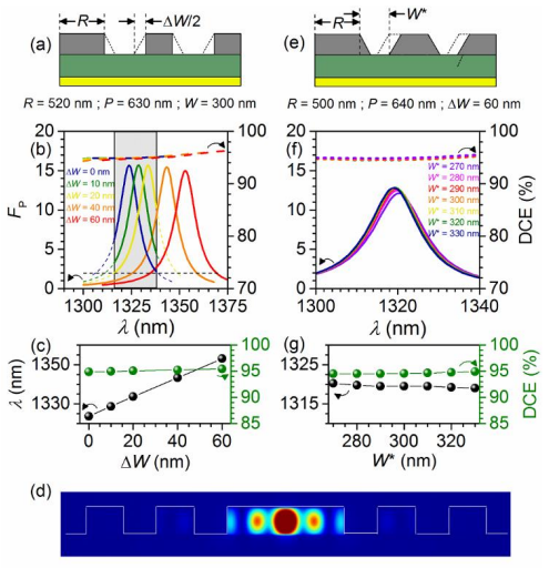
The central object is the hybrid circular Bragg grating: a central GaAs disc (radius around 520–550 nm) surrounded by concentric grating rings (period around 500–630 nm, gap width around 160–300 nm) on a SiO2 spacer around 300 nm thick, above a gold back-reflector. The gold mirror and spacer turn downward emission upward, while the periodic rings collimate the mode into a directional far-field. The argument runs on frequency-domain finite-element simulations that exploit rotational symmetry to reduce the problem to a two-dimensional cross-section, with the quantum dot modeled as a classical TE dipole; the key computed observables are the Purcell factor, the dipole-power collection efficiency into NA = 0.8, and the mode-coupling efficiency to a single-mode fiber. The design rules—increasing the gap width blue-shifts the resonance, increasing the period red-shifts it, and the disc radius controls confinement—allow the same performance to be reached with relaxed fabrication constraints.
What would settle it
Fabricate the broadband design (W = 300 nm, three rings) with a deterministically positioned InGaAs quantum dot, measure the emitter lifetime and the fraction of emission collected by an NA = 0.8 objective at about 1320 nm, and compare with the predicted Purcell factor near 15 and collection efficiency near 95%; if finite dot size, phonon sidebands, or strong-coupling corrections move either figure outside the reported tolerance, the central claim needs revision.
Extended reading notes
Core claim
The paper's central claim is that a hybrid circular Bragg grating—a GaAs central disc and concentric grating rings on a SiO2 spacer above a gold mirror—can be optimized so that a dipole emitter at the disc center emits more than 95% of its power into a collection NA of 0.8 while experiencing a Purcell factor near 30 at a wavelength around 1320 nm. Two parameter families are reported: a narrowband design (11 rings, gap width 160 nm) with a Purcell factor near 30 and a spectral width of 3.3 nm, and a broadband design (larger gap, fewer rings) with a Purcell factor near 15 and a spectral width of 11.9 nm. The broadband design is less demanding for lithography and better suited for enhancing both X and XX transitions in a biexciton-exciton cascade. The simulated performance degrades only mildly under tilted sidewalls and lateral emitter displacements within reported fabrication accuracy, and fiber coupling to a commercial 980HP fiber reaches 76–77% in vacuum. The load-bearing combination is simultaneous high extraction efficiency and high Purcell enhancement without requiring fragile free-standing membranes.
Load-bearing premise
The whole performance prediction rests on treating the quantum dot as a point-like classical dipole in the weak-coupling regime, meaning the simulated Purcell factor and collection efficiency are assumed to represent the real quantum emitter's behavior.
Editorial extensions
If this is right
- Operating at the telecom O-band makes these sources compatible with low-loss silica fiber networks, enabling long-distance quantum communication.
- The broadband design, with a Purcell factor near 15 over a 12 nm spectral range, can enhance both X and XX transitions of a biexciton cascade, supporting entangled-photon-pair generation.
- Fiber coupling efficiencies of 76–77% to an off-the-shelf 980HP fiber, with robustness to sidewall tilt, suggest that plug-and-play fiber-coupled sources are achievable.
- The systematic dependence of the operation wavelength on grating period and gap width provides a tuning recipe to match any O-band wavelength.
- A collection NA of only 0.4 still captures about 88% of the dipole power, relaxing experimental collection constraints.
Reading between the lines
- If the simulated robustness holds, hybrid circular Bragg gratings could replace free-standing membrane devices and micropillar cavities for telecom quantum sources, combining Purcell enhancement and broadband collection without undercut etching.
- The same parameter map could be re-optimized for other telecom bands, such as the C-band near 1550 nm, by scaling the period, gap width, and disc radius; the reported shift rules turn this into a parameter search rather than a conceptual redesign.
- A direct testable extension is to compare the classical-dipole finite-element predictions against a microscopic quantum model that includes phonon-mediated coupling and finite dot size; agreement would validate using the simulated Purcell factor and collection efficiency as quantum-optical figures of merit.
- The plateau in mode coupling efficiency for small fiber distances suggests that adhesive bonding at distances below 4 µm should be explored experimentally as a stable packaging route.
Signed reviews
Editorial analysis
A structured set of objections, weighed in public.
Referee Report
Summary. This manuscript reports a finite-element-method (FEM) design study of hybrid circular Bragg grating (CBG) quantum light sources operating in the telecom O-band around 1320 nm. The authors optimize a GaAs/SiO2/Au layer stack with a central disc and surrounding Bragg rings, specifying all geometric parameters (layer thicknesses, disc radius, grating period, gap width, ring number). They report dipole power extraction efficiencies (DCE) exceeding 95% into NA=0.8, Purcell factors close to 30 for a narrowband 11-ring design, and Purcell factors around 15 for a broadband design with a larger gap width. They investigate robustness to sidewall tilt and to lateral emitter displacement, and they simulate direct coupling to commercially available single-mode fibers (980HP and SMF28), reporting mode coupling efficiencies up to about 77%. The paper concludes that such designs are promising for robust, near-ideal, fiber-coupled quantum light sources for long-distance quantum communication.
Significance. If the reported numbers hold, this design study provides a concrete and useful blueprint for telecom-wavelength quantum light sources with near-unity extraction and strong Purcell enhancement, which is directly relevant for quantum communication applications. The strengths of the paper are its systematic parameter sweeps, fully specified geometry and material parameters, use of published refractive-index data rather than fitted parameters, and the inclusion of detailed robustness studies for sidewall tilts and emitter displacements. The 3D displacement study and the fiber-coupling analysis are particularly valuable. However, the headline combination of the highest Purcell factor and extraction efficiency, on the one hand, and the demonstrated robustness, on the other hand, is obtained on different device variants; this gap in evidence needs to be addressed before the abstract-level claims can be accepted as stated.
major comments (2)
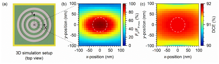
- [Fabrication robustness / Fig. 3] The 3D emitter-displacement robustness study is performed only on the broadband design with three Bragg rings (FP ~15, DCE ~92%), as explicitly stated in the text near Fig. 3(a). The narrowband 11-ring design that delivers the headline values (FP close to 30, DCE >95%) has a different mode profile concentrated near the disc edge (Fig. 2(d)) and a higher Q-factor, so its sensitivity to a 34 nm lateral emitter displacement cannot be inferred from the broadband simulation. The abstract and conclusion generalize the robustness statement to 'the designs', but the evidence directly supports only the broadband variant. This is load-bearing because the central message combines high performance with robustness; please either perform the equivalent 3D displacement simulation for the narrowband design (or a computationally tractable reduced-ring variant with a stated correction) or explicitly restrict the robustness claim to the broadband design.
- [Fabrication robustness / Fig. 2] The sidewall-tilt robustness analysis in Fig. 2 is also performed only for the broadband design with target gap width W=300 nm. The narrowband 11-ring design (W=160 nm, R=550 nm, P=500 nm) is not tested for tilted sidewalls, even though its narrower gaps and higher sensitivity of the resonance wavelength to geometric changes make it the more critical case. The conclusion that 'our designs proved to be robust' therefore overstates the coverage of the parameter space. Please either add a tilt study for the narrowband design or temper the conclusion to specify that the demonstrated sidewall robustness applies to the broadband design.
minor comments (5)
- [Abstract / Conclusion] The abstract states coupling efficiencies of 'up to 77%' while the conclusion states 'mode-coupling efficiencies close to 80%'; the maximum MCE reported in the main text is 76.9%. These numbers should be harmonized to avoid an apparent inconsistency.
- [Abstract] The phrase 'and again proof robustness' should be 'and again prove robustness'.
- [References] Reference [36] contains a typo: 'J.-M. Gérad' should be 'J.-M. Gérard'. Reference [38] lists 'P. Lohdal' and should be 'P. Lodahl'. Additionally, reference [10] and reference [32] are duplicates of the same Dousse et al. 2008 paper and should be consolidated.
- [Emitter displacement discussion (Fig. 3)] The text speculates about the behavior for emitters emitting a mixture of both polarizations and states that the mode near-field would be circularly symmetric; since the simulations use a linearly polarized dipole, this statement is not directly supported by the presented simulations and should be clearly labeled as an expectation rather than a simulated result.
- [Supplementary Fig. 5(a) caption] The sentence 'A FP close to 30 (above 15) and a DCE of over 90% is reached' is grammatically ambiguous; please clarify which parenthetical value corresponds to which device variant (narrowband versus broadband).
Circularity Check
No significant circularity: the reported DCE, Purcell factors, and fiber-coupling efficiencies are direct outputs of FEM simulations with explicitly stated geometries, not re-statements of fitted inputs or self-citation chains.
full rationale
The paper's central claims derive from frequency-domain FEM simulations performed in JCMsuite for a fully specified hybrid CBG geometry. The design parameters (t(Au), t(SiO2), t(GaAs), R, P, W, number of rings) are varied in a parameter study, and the reported figures of merit are computed quantities: DCE is the integrated far-field power into NA=0.8 divided by the total dipole power, PCE is the same power divided by the power emitted into the upper half space, and the Purcell factor is obtained from the simulated mode. None of these quantities is fitted to the target result and then re-presented as a prediction; the geometry is not defined in terms of the achieved DCE, Purcell factor, or MCE. The fiber-coupling study likewise computes a mode overlap between the simulated CBG near-field and the fiber mode, and the robustness studies vary sidewall tilt and emitter displacement as independent perturbations. The manuscript's self-citations are used for methodological context and for experimentally demonstrated positioning accuracies; they do not supply the load-bearing numerical results, and no uniqueness theorem or ansatz is imported from the authors' prior work to force the chosen design. The only notable gap is that the lateral-displacement robustness simulation is performed on the 3-ring broadband design rather than the 11-ring narrowband design, but this is a scope limitation of the evidence, not a circular reduction of the prediction to its input. The weak-coupling assumption is stated explicitly as a modeling premise and does not make any output equal its input by construction. No circular step satisfying the quoted-evidence requirement was found.
Assumptions & free parameters
assumptions (6)
- standard math Maxwell's equations govern the optical mode and are solved by the finite element method in the frequency domain.
- domain assumption Material refractive indices at lambda=1320 nm (GaAs n=3.3885, SiO2 n=1.4500, Au n=0.3970+8.9523i) are correct and remain valid after a ~10 nm blue-shift correction for cryogenic operation.
- domain assumption The quantum emitter can be modeled as a classical TE dipole source placed at the center of the central disc.
- domain assumption The weak-coupling regime is valid for all studied designs (Q-factor up to 800).
- domain assumption Most simulations can be reduced to a two-dimensional rotationally symmetric cross-section; full 3D is needed only for emitter displacement.
- standard math Perfectly matched layer (PML) boundaries correctly absorb outgoing radiation without perturbing the mode.
Cite this review
Pith. "Pith review of Optimized Designs for Telecom-Wavelength Quantum Light Sources Based on Hybrid Circular Bragg Gratings." pith.science (2026). https://pith.science/paper/OQVOEMON
@misc{pith2026190808408,
  author       = {Pith},
  title        = {Pith review of: Optimized Designs for Telecom-Wavelength Quantum Light Sources Based on Hybrid Circular Bragg Gratings},
  year         = {2026},
  howpublished = {\url{https://pith.science/paper/OQVOEMON}},
  note         = {Machine review of arXiv:1908.08408}
}
read the original abstract
We present a design study of quantum light sources based on hybrid circular Bragg Gratings (CBGs) for emission wavelengths in the telecom O-band. The evaluated CBG designs show photon extraction efficiencies > 95% and Purcell factors close to 30. Using simulations based on the finite element method, and considering the influence of possible fabrication imperfections, we identify optimized high-performance CBG designs which are robust against structural aberrations. In particular, full 3D simulations reveal that the designs show robustness regarding deviations of the emitter position in the device well within reported positioning accuracies of deterministic fabrication technologies. Furthermore, we investigate the coupling of the evaluated hybrid CBG designs to single-mode optical fibers, which is particularly interesting for the development of practical quantum light sources. We obtain coupling efficiencies of up to 77% for off-the-shelf fibers, and again proof robustness against fabrication imperfections. Our results show prospects for the fabrication of close-to-ideal fiber-coupled quantum light sources for long distance quantum communication.
Figures

Figures from the paper (1 more)

Reference graph
Works this paper leans on
-
[1]
J. L. O'Brien, A. Furusawa, and J. Vučković, Nat. Photonics 3, 687-695 (2009)
work page 2009
-
[2]
I. Aharonovich, D. Englund, and M. Toth, Nat. Photonics 10, 631 -641 (2016)
work page 2016
-
[3]
A. Acín, I. Bloch, H. Buhrman, T. Calarco, C. Eichler, and J. Eisert, New J. Phys. 20, 80201 (2018)
work page 2018
- [4]
-
[5]
E. Waks, K. Inoue, C. Santori, D. Fattal, J. Vučković, G. Solomon, and Y. Yamamoto, Nature 420, 762 (2002)
work page 2002
-
[6]
H.-K. Lo, M. Curty, and K. Tamaki, Nat. Photonics 8, 595-604 (2014)
work page 2014
-
[7]
R. Raussendorf and H. J. Briegel, Phys. Rev. Lett. 86, 5188-5191 (2001)
work page 2001
-
[8]
P. Kok, W. J. Munro, K. Nemoto, T. C. Ralph, J. P. Dowling, and G. J. Milburn, Rev. Mod. Phys. 79, 135-174 (2007)
work page 2007
Show all 39 references
-
[9]
T. D. Ladd, F. Jelezko, R. Laflamme, Y. Nakamura, C. Monroe, and J. L. O'Brien, Nature 464, 45 -53 (2010)
2010
-
[11]
Gschrey, F
M. Gschrey, F. Gericke, A. Schüßler, R. Schmidt, J.-H. Schulze, T. Heindel, S. Rodt, A. Strittmatter, and S. Reitzenstein, Appl. Phys. Lett. 102, 251113 (2013)
2013
-
[12]
J. Liu, M. I. Darvanço, L. Sapienza, K. Konthasinghe, J. V. De Miranda Cardo so, J. D. Song, A. Badolato, and K. Srinivasan, Rev. Sci. Instrum. 88, 23116 (2017)
2017
-
[13]
Heindel, S
T. Heindel, S. Rodt, and S. Reitzenstein, in Quantum Dots for Quantum Information Technologies, edited by P. Michler (Springer International Publishing, Cham, 2017), p. 199
2017
-
[14]
S. Hepp, M. Jetter, S. L. Portalupi, and P. Michler, Adv. Quantum Technol. 9, 1900020 (2019)
2019
-
[15]
Reitzenstein and A
S. Reitzenstein and A. Forchel, J. Phys. D: Appl. Phys. 43, 33001 (2010)
2010
-
[16]
Heindel, C
T. Heindel, C. Schneider, M. Lermer, S. H. Kwon, T. Braun, S. Reitzenstein, S. Höflin g, M. Kamp, and A. Forchel, Appl. Phys. Lett. 96, 011107 (2010)
2010
-
[17]
Gazzano, S
O. Gazzano, S. M. de Vasconcellos, C. Arnold, A. Nowak, E. Galopin, I. Sagnes, L. Lanco, A. Lemaître, and P. Senellart, Nat. Commun. 4, 1425 (2013)
2013
-
[18]
Wang, Z.-C
H. Wang, Z.-C. Duan, Y.-H. Li, S. Chen, J.-P- Lim, Y.-M- He, M.-C. Chen, Y. Hu, X. Ding et al., Phys. Rev. Lett. 116, 213601 (2016)
2016
-
[19]
Akopian, N
N. Akopian, N. H. Lindner, E. Poem, Y. Berlatzky, J. Avron, D. Gershoni, B. D. Gerardot, and P. M. Petroff, Phys. Rev. Lett.. 96, 130501 (2006)
2006
-
[20]
Heindel, A
T. Heindel, A. Thoma, I. Schwartz, E. R. Schmidgall, L. Gantz, D. Cogan, M. Strauß, P. Schnauber, M. Gschrey, J.-H. Schulze, A. Strittmatter, S. Rodt, D. Gershoni, and S. Reitzenstein, APL Photonics 2, 121303 (2017)
2017
-
[21]
Gschrey, A
M. Gschrey, A. Thoma, P. Schnauber, M. Seifried, R. Schmidt, B. Wohlfeil, L. Krüger, J.-H. Schulze, T. Heindel, S. Burger, F. Schmidt, A. Strittmatter, S. Rodt, and S. Reitzenstein, Nat. Commun. 6, 7662 (2015)
2015
-
[22]
M. I. Davanço, M. T. Rakher, D. Schuh, A. Badolato, and K. Srinivasan, Appl. Phys. Lett. 99, 41102 (2011 )
2011
-
[23]
B. Yao, R. Su, Y. Wei, Z. Liu, T. Zhao, and J. Liu, J. Korean Phys. Soc. 73, 1502 (2018)
2018
-
[24]
J. Liu, R. Su, Y. Wei, B. Yao, S. F. C. da Silva, Y. Yu, J. Iles-Smith, K. Srinivasan, A. Rastelli, J. Li and X. Wang, Nat. Nanotechnol. 14, 586-593 (2019)
2019
-
[25]
H. Wang, H. Hai, T.-H. Chung, J. Qin, L. Xiaoxia, J.-P- Li, R.-Z. Liu, H.-S. Zhong, Y.-M. He, X. Ding, Y.-H. Deng, Q. Dai, Y.-H. Huo, S. Höfling, C.-Y. Lu, and J.-W. Pan, Phys. Rev. Lett. 122, 113602 (2019)
2019
-
[26]
Simulation Suite for Nano-Optics (JCMwave GmbH, Berlin, 2019)
JCMsuite by JCMwave. Simulation Suite for Nano-Optics (JCMwave GmbH, Berlin, 2019)
2019
-
[27]
Schneider, N
P.-I. Schneider, N. Srocka, S. Rodt, L Zschiedrich, S. Reitzenstein, and S. Burger, Optics Exp. 26, 8479 (2018)
2018
-
[28]
Thoma, P
A. Thoma, P. Schnauber, M. Gschrey, M. Seifried, J. Wolters, J.-H. Schulze, A. Strittmatter, S. Rodt, A. Carmele, A. Knorr, T. Heindel, and S. Reitzenstein, Phys. Rev. Lett. 116, 033601 (2016)
2016
-
[29]
M. Paul, J. Kettler, K. Zeuner, C. Clausen, M. Jetter, and P. Michler, Appl. Phys. Lett. 106, 122105 (2015)
2015
-
[30]
Gschrey, R
M. Gschrey, R. Schmidt, J.-H. Schulze, A. Strittmatter, S. Rodt, and S. Reitzenstein, J. Vac. Sci. B 33, 021603 (2015)
2015
-
[31]
J. Liu, M. I. Davanço, L. Sapienza, K. Konthasinghe, J. V. D. M. Cardoso, J. D. Song, A. B adolato, and K. Srinivasan, Rev. Sci. Instrum. 88, 023116 (2017)
2017
-
[32]
Dousse, L
A. Dousse, L. Lanco, J. Suffczyński, E. Semenova, A. Miard, A. Lemaître, I. Sagnes, C. Roblin, J. Bloch, and P. Senellart, Phys. Rev. Lett. 101, 267404 (2008)
2008
-
[33]
Norland Products Inc., Norland Optical Adhesive 81
-
[34]
Schlehahn, S
A. Schlehahn, S. Fischbach, R. Schmidt, A. Kagansky, A. Strittmatter, S. Rodt, T. Heindel, and S. Reitzenstein, Sci. Rep. 8, 1340 (2018)
2018
-
[35]
Snijders, J
H. Snijders, J. A. Frey, J. Norman, V. P. Post, A. C. Gossard, J. E. Bowers, M. P. van Exter, W. Löffler, and D. Bouwmeester, Phys. Rev. Applied 9, 031002 (2018)
2018
-
[36]
Cadeddu, J
D. Cadeddu, J. Teissier, F. R. Braakman, N. Gregersen, P. Stepanov, J.-M. Gérad, J. Claudon, R. J. Warburton, M. Poggi, M. Munsch, Appl. Phys. Lett. 108, 11112 (2016)
2016
-
[37]
Lee, H.-J
C.-M. Lee, H.-J. Lim, C. Schneider, S. Maier, S. Höfling, M. Kamp, and Y.-H. Lee, Sci. Rep. 5, 14309 (2015)
2015
-
[38]
Further improvements in the coupling performance are expected, e.g
and micropillar structures [35]. Further improvements in the coupling performance are expected, e.g. by optimizing the combined design parameters of hybrid CBG devices using optimization algorithms [39] and specialty fibers with tailored geometry and index profiles. Last but n...
-
[39]
R. S. Daveau, K. C. Balram, T. Pregnolato, J. Liu, E. H. Lee, J. D. Song, V. Verma, R. Mirin, S. W. Nam, L. Midolo, S. Stobbe, K. Srinivasan, P. Lohdal, Optica 4, 178-184 (2017)
2017
-
[40]
Schneider, X
P.-I. Schneider, X. G. Santiago, V. Soltwitsch, M. Hammerschmidt, S. Burger, and C. Rockstuhl, ACS Photonics, doi: 10.1021/acsphotonics.9b00706 Supplementary Material Figure 5 – complementing Fig. 1(e) and 1(f): (a) Maximum Purcell factor FP and dipole power collection efficie...
Reviewed August 14, 2026 · model on record in the stance chip above.
Discussion (0). Continue with ORCID to comment.