REVIEW 3 major objections 4 minor 140 references
Etude des proprietes optoelectroniques de nanocristaux colloidaux a faible bande interdite : application a la detection infrarouge
T0 review · 3 major / 4 minor · reviewed 2026-08-14 · deepseek-v4-flash
Pith's one-line read HgSe nanocrystals become metallic as their size increases, and a HgTe diode detects 2.5 µm infrared light at 20 mA/W with 3×10^9 Jones detectivity.
desk verdict A solid thesis compilation of HgTe/HgSe nanocrystal work, but the semiconductor-metal transition claim rests on fitted k.p parameters and film-level transport that does not independently prove per-particle metallicity. read the letter →
The pith
A machine-rendered reading of the paper's core claim, the machinery that carries it, and where it could break.
The reading
What carries the argument
The load-bearing tool is the reconstructed absolute electronic structure of the nanocrystals, built from three complementary measurements plus one model. X-ray photoemission gives the Fermi level and work function; infrared absorption gives the 1Se–1Pe intraband and 1Sh–1Se interband transitions; and a three-band k.p model, with fitted parameters $E_{\Gamma6-\Gamma8} = -0.2$ eV and $E_p = 10.3$ eV for HgSe, places the 1De level. Because the conduction levels in these inverted-gap materials are approximately $\hbar^2\pi^2/(2m_e^* R^2)$ above the band edge, the level on which the Fermi energy sits directly counts electrons per nanocrystal (2, 8, and 18 for 1Se, 1Pe, and 1De). The same machinery yields a phase diagram of doping versus confinement and guides the diode design by providing band energies for contact selection.
What would settle it
Electrochemically titrate the electron count per HgSe nanocrystal as a function of diameter and compare with the predicted occupations of 2, 8, and 18 electrons; if the counts do not step at the claimed sizes, the k.p-derived phase diagram and the size-driven semiconductor-metal transition are unsupported.
Extended reading notes
Core claim
On the paper's own terms, the central discovery is a size- and surface-dependent electronic phase diagram for HgSe and HgTe nanocrystals. The author reconstructs the full electronic structure from photoemission (Fermi level, work function, valence-band edge), FTIR (interband and intraband transitions), and a three-band k.p calculation of the higher conduction levels. For HgSe, the Fermi level lies above the 1Se level for 4.5 nm particles, above 1Pe for 5.8 nm particles, and above 1De for 17 nm particles, corresponding to roughly 2, 8, and 18 electrons per nanocrystal. This is a semiconductor-to-metal transition driven by decreasing confinement rather than by added dopants, corroborated by the intraband peak becoming a temperature-insensitive plasmon and by the low-temperature hopping exponent switching from Mott ($T^{-1}$/4) to Efros-Shklovskii ($T^{-1}$/2). Surface ligands act as a second control knob: dipolar ligands such as S2− lower the Fermi level and switch interband transitions back on, and electron-accepting polyoxometalate ligands reduce the HgSe doping to 0.03 electron per nanocrystal. The device payoff is a HgTe photodiode in the extended short-wave infrared: a 100-pixel array images a laser profile, and single pixels give 20 mA/W response and 3×$10^{9}$ Jones detectivity at 2.5 µm. The author notes that even the most doped HgSe films remain semiconducting in their resistance-temperature behavior because interparticle transport is still hopping, so the metallicity is per-particle.
Load-bearing premise
The quantitative doping levels and the semiconductor-metal transition rest on the fitted three-band k.p parameters for HgSe ($E_{\Gamma6-\Gamma8} = -0.2$ eV and $E_p = 10.3$ eV) being size-independent, and on reading per-particle metallicity from film-level hopping exponents.
Editorial extensions
If this is right
- HgSe nanocrystals of controlled size offer tunable mid- to far-infrared plasmonic resonances with carrier densities near 10^18 cm^-3, lower than in doped oxide nanocrystals, so the same material can serve as an intraband absorber or a plasmonic element.
- Surface-chemistry doping gives a post-synthesis route to p-type or ambipolar mercury-chalcogenide films, useful for reducing dark current and for building junctions without introducing impurity atoms.
- The measured absolute band energies and work functions for HgTe allow rational electrode and barrier selection, which the author uses to reach a photoresponse of 20 mA/W and a detectivity of 3×10^9 Jones at 2.5 µm.
- The ink-based phase-transfer ligand exchange produces thicker absorbing layers (around 500 nm) than layer-by-layer film exchange, simplifying fabrication of vertical photodiodes.
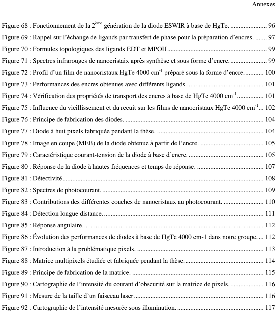
- A 100-pixel HgTe nanocrystal array can reconstruct an infrared laser intensity profile, a proof-of-concept step toward nanocrystal-based infrared cameras.
Reading between the lines
- The same size-driven Fermi-level rise may occur in other zero-gap or inverted-gap nanocrystals; a testable extension is to map doping versus diameter in HgS and Ag2Se using the same photoemission-plus-infrared reconstruction.
- The electron counts 2, 8, and 18 correspond to shell filling, so Coulomb-blockade or electrochemical charging experiments could test whether the transition steps through discrete shell occupations, refining the phase diagram beyond the continuum k.p model.
- Oxidative polyoxometalate ligands could be generalized to produce stable p-type films from other self-doped nanocrystals; a concrete test is to combine them with a strongly dipolar n-type ligand on the same batch to form a ligand-defined p-n junction.
- The transient-photocurrent Urbach measurement is faster than optical sub-gap absorption and, if it transfers to other materials, gives a practical passivation-quality metric for nanocrystal films.
Signed reviews
Editorial analysis
A structured set of objections, weighed in public.
Referee Report
Summary. This PhD thesis, written in French, studies the optoelectronic properties of colloidal HgSe and HgTe nanocrystals for infrared detection. The central claims are that the Fermi level and doping level of HgSe nanocrystals can be controlled by quantum confinement and by surface ligand chemistry, that HgSe undergoes a size-driven semiconductor-to-metal transition with the electron count increasing from about 2 to 18 electrons per nanocrystal as the diameter grows from 4.5 to 17 nm, and that a HgTe-based photodiode assembled from nanocrystal inks detects 2.5 µm light with a photoresponse of 20 mA/W and a detectivity of 3x10^9 Jones. The manuscript reconstructs the electronic structure using X-ray photoemission, infrared absorption, field-effect transport, and a three-band k.p model, and it also presents an original transient-photocurrent method for measuring the Urbach energy, a redox-doping study using polyoxometalate ligands, and a 100-pixel HgTe imager prototype.
Significance. If the electronic-structure reconstruction is valid, the thesis provides a coherent and useful picture of how confinement and surface chemistry tune doping in narrow-gap colloidal nanocrystals. The main experimental strengths are direct photoemission measurements of absolute level positions and work functions, systematic size- and ligand-dependent spectroscopy, a transient-photocurrent method for trap distributions, XPS evidence for electron transfer to polyoxometalate ligands, and a demonstrated SWIR photodiode with a multipixel array. These are concrete, falsifiable results that go beyond a purely phenomenological study. The weak point is that the quantitative doping counts and the semiconductor-to-metal transition rest on a k.p model fitted to the same class of intraband transitions that the model is then used to interpret; this is a parameterized consistency argument rather than an independent determination. The device-oriented chapters and the ligand-doping control are largely independent of that fragility and appear sound.
major comments (3)
- [Ch. 2, §II.2.b.ii (Eq. 2.12)] The electron counts per nanocrystal, and hence the claimed semiconductor-to-metal transition, are quantitatively set by the position of the 1De level calculated from the three-band k.p model. The parameters EΓ6-Γ8 = -0.2 eV and Ep = 10.3 eV are obtained by fitting intraband transition energies from the literature and from the author's own measurements. Using these fitted levels to interpret the same type of intraband data, and to infer 2, 8, or 18 electrons per nanocrystal, is a fit-to-data consistency check, not an independent prediction. The manuscript gives no uncertainty bars on the fitted parameters, no test of their size independence, and no alternative determination of the doping level. I therefore regard the quantitative 18-electron count and the precise location of the semiconductor-to-metal boundary as not fully supported, even though the qualitative trend of increasing n-type doping with decreasing confinement is plausible from the direct photoemission data.
- [Ch. 2, §II.3.b (Fig. 46)] The transport measurements are presented as validating the semiconductor-to-metal transition, but the T^-1/4 (Mott) versus T^-1/2 (Efros-Shklovskii) analysis distinguishes two hopping regimes and does not by itself establish that the individual particles are metallic. The manuscript explicitly states that the film resistance still decreases with increasing temperature in both cases, i.e., the film remains semiconducting, so the metal-insulator transition is claimed at the per-particle level while the measured quantity is a film-level property. This evidence is therefore weaker than the text suggests and cannot independently compensate for the uncertainty in the k.p-based doping levels. The authors should either soften the transport-based confirmation, provide an explicit model showing how per-particle metallicity maps onto the observed exponent, or add independent per-particle evidence such as gate-dependent spectroscopy or single-nanocrystal measurements.
- [Ch. 2, §II.3.a (Eq. 2.13)] The infrared plasmon check is an order-of-magnitude consistency test, not an independent cross-check. The carrier density obtained from the plasmon frequency (6.3x10^18 cm^-3) is compared with the value inferred from the k.p-based level occupancy (4.5x10^18 cm^-3), but both estimates use the same effective mass and the same electronic-structure model. The agreement to within a factor of about 1.4 confirms that the measured intraband feature is compatible with a collective plasmon, but it does not add independent support for the 18-electron count. This should be stated more cautiously in the conclusions of Chapter 2.
minor comments (4)
- [Notations et abréviations (p. 5)] The heading contains a typo: 'Abréviatons' should be 'Abréviations'.
- [Ch. 4, heading and opening paragraph of Section I] The phrase 'dans le but de construire une caméra et donc, et donc d'être capable de reconstruire une image' contains a duplicated 'et donc'; one occurrence should be removed.
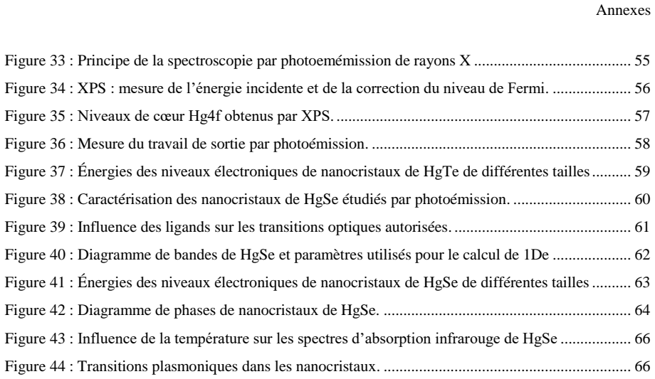
- [Ch. 2, Fig. 41 and Fig. 42] The figure captions do not state the k.p model parameters used to place the 1De level, nor the assumed degeneracies (2, 6, 10 electrons) underlying the doping counts. Adding this information in the captions would make the derivation easier to audit.
- [Ch. 3, Eq. (3.2)] The thermal-activation expression n = 2 exp(-(E1Se - EF)/kBT) is introduced without derivation; the prefactor of 2 deserves a brief explanation (spin degeneracy or level degeneracy) so that the resulting 0.03-electron estimate is reproducible.
Circularity Check
HgSe metallicity and electron count are partly model-forced: the 1De level is computed from the same k.p parameters fitted to intraband data; transport exponents do not independently establish per-particle metallicity.
-
fitted input called prediction
[Chapter 2, Section II.2.b.ii (Equation 2.12), used in Section II.2.b.iii and the Figure 42 phase diagram]
"Les seuls paramètres de cette équation sont EΓ6-Γ8 et Ep, que l'on peut déterminer par simulation. En ajoutant les résultats de la littérature à nos données pour les valeurs des transitions intrabandes dans HgSe à différentes tailles(49, 51), j'obtiens que EΓ6-Γ8 vaut -0,2 eV et Ep vaut 10,3 eV pour HgSe. ... Les valeurs des transitions 1De – 1Pe sont ensuite obtenues en utilisant les valeurs de k correspondant à ces niveaux ... soit 4,49/R pour 1Pe et 5,76/R pour 1De."
The 1De level is the quantity that, when crossed by the measured Fermi level, yields the 18-electron/metallic state for the 17 nm HgSe nanocrystals (Figure 42). But 1De is not measured: it is computed from Eq. (2.12) using EΓ6-Γ8 = -0.2 eV and Ep = 10.3 eV, two parameters just fitted to intraband transition data of the same HgSe nanocrystal family, including the author's own data. The electron-count ladder (2, 8, 18 e-) and the size at which the semiconductor-metal crossover occurs are therefore in-sample outputs of that calibration, not independent predictions. The photoemission Fermi level and optical transitions are measured independently, so the circularity is partial, but the quantitative metallicity claim is not self-contained.
full rationale
The thesis rests on several independent experimental measurements: XPS gives absolute Fermi-level and work-function positions; FTIR gives interband and intraband transitions; FET and electrochemistry give carrier-type; and the E-SWIR diode photoresponse is directly measured. None of those results reduce by definition to the claimed outputs. The main circularity-adjacent step is the HgSe electron-count/metallicity ladder. The 1De energy that separates the 8-electron and 18-electron regimes is not measured but computed from the two-parameter k.p dispersion of Eq. (2.12), and those two parameters were calibrated on intraband transition energies from the same HgSe nanocrystal system. Consequently the 18-electron count and the size-driven semiconductor-metal crossover are partly model-forced outputs rather than out-of-sample predictions. The infrared plasmon cross-check is only order-of-magnitude and uses the same effective-mass input. In addition, the transport validation is weaker than claimed: the manuscript itself admits the film resistance still has a semiconducting temperature dependence, so the Mott versus Efros-Shklovskii exponents distinguish hopping regimes, not per-particle metallic versus semiconducting behavior. This is a correctness caveat rather than a circular step. Self-citations appear frequently but are used as data sources and prior measurements, not as load-bearing authority to forbid alternatives. Overall, the central direct experimental claims are self-contained, but the quantitative semiconductor-metal transition in HgSe is partially constructed from the fitted k.p parameters, giving a score of 4.
Assumptions & free parameters
free parameters (4)
- EΓ6-Γ8 (mercury selenide k.p gap) =
-0.2 eV
- Ep (Kane energy) =
10.3 eV
- Urbach power-law exponent b =
-0.27 (for EDT ligand)
- Hooge constant alpha =
not numerically specified
assumptions (4)
- domain assumption Effective mass and k.p approximations describe the conduction band of HgSe nanocrystals across the investigated size range.
- domain assumption Mott (T^-1/4) and Efros-Shklovskii (T^-1/2) variable-range hopping regimes can be used to infer the metallic or semiconducting character of individual nanoparticles from film transport.
- domain assumption The transient photocurrent power-law decay reflects an exponential Urbach tail of trap states, and Eu = kBT/(b+1) holds.
- ad hoc to paper HgSe nanocrystal self-doping arises from a redox reaction with ambient water/oxygen because the 1Se level lies below the O2/H2O potential.
Cite this review
Pith. "Pith review of Etude des proprietes optoelectroniques de nanocristaux colloidaux a faible bande interdite : application a la detection infrarouge." pith.science (2026). https://pith.science/paper/BTYHDVGV
@misc{pith2026190808849,
  author       = {Pith},
  title        = {Pith review of: Etude des proprietes optoelectroniques de nanocristaux colloidaux a faible bande interdite : application a la detection infrarouge},
  year         = {2026},
  howpublished = {\url{https://pith.science/paper/BTYHDVGV}},
  note         = {Machine review of arXiv:1908.08849}
}
read the original abstract
Colloidal semiconductor nanocrystals are nanomaterials synthesized in solution. Below a certain size, these nanocrystals acquire quantum confinement properties: their optoelectronic properties depend on the nanoparticle size. In the visible range, colloidal nanocrystals are quite mature. The next objective in this field is to get infrared colloidal nanocrystals. Mercury selenide (HgSe) and mercury telluride (HgTe) are potential candidates. The goal of this PhD work is to strengthen our knowledge on optical, optoelectronic and transport properties of these nanocrystals, in order to design an infrared detector. To do so, we studied the electronic structure of HgSe and HgTe for different sizes and surface chemistries. We can then determine the energies of the electronic levels and the Fermi energy, quantify doping level. We show that the nanocrystal size has an influence on doping level, which gets more and more n-type as the nanocrystal size gets larger. We even observe a semiconductor-metal transition in HgSe nanocrystals as the size is increased. The doping control with surface chemistry is then investigated. By using dipolar effects or oxidizing ligands, we show a doping control over several orders of magnitude. Thanks to these studies, we are able to propose a HgTe based device for detection at 2,5 um, which structure allows to convert effectively the absorbed photons into an electrical current and to get a high signal over noise ratio. We get a photoresponse of 20 mA/W and a detectivity of 3.10^9 Jones.
Figures
Reference graph
Works this paper leans on
-
[1]
The Bakerian Lecture
Faraday Michael, X. The Bakerian Lecture. —Experimental relations of gold (and other metals) to light. Philos. Trans. R. Soc. Lond. 147, 145–181 (1857)
-
[2]
Mie, Beiträge zur Optik trüber Medien, speziell kolloidaler Metallösungen
G. Mie, Beiträge zur Optik trüber Medien, speziell kolloidaler Metallösungen. Ann. Phys. 330, 377–445 (1908)
1908
-
[3]
Delerue, D
C. Delerue, D. Vanmaekelbergh, Electronic band structure of zinc blende CdSe and rock salt PbSe semiconductors with silicene-type honeycomb geometry. 2D Mater. 2, 34008 (2015)
2015
-
[4]
Benchamekh, N
R. Benchamekh, N. A. Gippius, J. Even, M. O. Nestoklon, J. -M. Jancu, S. Ithurria, B. Dubertret, A. L. Efros, P. Voisin, Tight -binding calculations of image -charge effects in colloidal nanoscale platelets of CdSe. Phys. Rev. B. 89, 35307 (2014)
2014
-
[5]
Kittel, Théorie quantique du solide (Dunod, 1967)
C. Kittel, Théorie quantique du solide (Dunod, 1967)
1967
-
[6]
Hill, Energy-gap variations in semiconductor alloys
R. Hill, Energy-gap variations in semiconductor alloys. J. Phys. C Solid State Phys. 7, 521–526 (1974)
1974
-
[7]
Sadao, GaAs And Related Materials (World Scientific, 1994)
A. Sadao, GaAs And Related Materials (World Scientific, 1994)
1994
-
[8]
Y. P. Varshni, Temperature dependence of the energy gap in semiconductors. Physica. 34, 149–154 (1967)
1967
Show all 140 references
-
[9]
V. I. Klimov, Semiconductor and Metal Nanocrystals: Synthesis and Electronic and Optical Properties (CRC Press, 2003)
2003
-
[10]
Rinnerbauer, K
V. Rinnerbauer, K. Hingerl, M. Kovalenko, W. Heiss, Effect of quantum confinement on higher transitions in HgTe nanocrystals. Appl. Phys. Lett. 89, 193114 (2006)
2006
-
[11]
Goubet, A
N. Goubet, A. Jagtap, C. Livache, B. Martinez, H. Portalès, X. Z. Xu, R. P. S. M. Lobo, B. Dubertret, E. Lhuillier, Terahertz HgTe Nanocrystals: Beyond Confinement. J. Am. Chem. Soc. 140, 5033–5036 (2018)
2018
-
[12]
J. M. Pietryga, Y. -S. Park, J. Lim, A. F. Fid ler, W. K. Bae, S. Brovelli, V. I. Klimov, Spectroscopic and Device Aspects of Nanocrystal Quantum Dots. Chem. Rev. 116, 10513 – 10622 (2016)
2016
-
[13]
C. B. Murray, D. J. Norris, M. G. Bawendi, Synthesis and characterization of nearly monodisperse CdE (E = sulf ur, selenium, tellurium) semiconductor nanocrystallites. J. Am. Chem. Soc. 115, 8706–8715 (1993)
1993
-
[14]
Jasieniak, L
J. Jasieniak, L. Smith, J. van Embden, P. Mulvaney, M. Califano, Re -examination of the Size - Dependent Absorption Properties of CdSe Quantum Dots. J. Phys. Chem. C. 113, 19468–19474 (2009)
2009
-
[15]
M. A. Hines, P. Guyot-Sionnest, Synthesis and Characterization of Strongly Luminescing ZnS- Capped CdSe Nanocrystals. J. Phys. Chem. 100, 468–471 (1996)
1996
-
[16]
Tamang, C
S. Tamang, C. Lincheneau, Y. Hermans, S. Jeong, P. Reiss, Chemistry of InP Nanocrystal Syntheses. Chem. Mater. 28, 2491–2506 (2016)
2016
-
[17]
J. L. Stein, E. A. Mader, B. M. Cossairt, Luminescent InP Quantum Dots with Tunable Emission by Post-Synthetic Modification with Lewis Acids. J. Phys. Chem. Lett. 7, 1315–1320 (2016)
2016
-
[18]
Nedelcu, L
G. Nedelcu, L. Protesescu, S. Yakunin, M. I. Bodnarchuk, M. J. Grotevent, M. V. Kovalenko, Fast Anion-Exchange in Highly Luminescent Nanocrystals of Cesium Lead Halide Perovskites (CsPbX3, X = Cl, Br, I). Nano Lett. 15, 5635–5640 (2015)
2015
-
[19]
B. G. Streetman, S. K. Banerjee, Solid State Electronic Devices (2014), Pearson
2014
-
[20]
M. A. Hines, G. D. Scholes, Colloidal PbS Nanocrystals with Size -Tunable Near -Infrared Emission: Observation of Post-Synthesis Self-Narrowing of the Particle Size Distribution. Adv. Mater. 15, 1844–1849 (2003)
2003
-
[21]
Y. Pan, Y. R. Li, Y. Zhao, D. L. Akins, Synthesis and Characterization of Quantum Dots: A Case Study Using PbS. J. Chem. Educ. 92, 1860–1865 (2015)
2015
-
[22]
Martinez, C
B. Martinez, C. Livache, L. D. Notemgnou Mouafo, N. Gou bet, S. Keuleyan, H. Cruguel, S. Ithurria, H. Aubin, A. Ouerghi, B. Doudin, E. Lacaze, B. Dubertret, M. G. Silly, R. P. S. M. Bibliographie 150 Lobo, J.-F. Dayen, E. Lhuillier, HgSe Self-Doped Nanocrystals as a Platform t...
2017
-
[23]
Allan, C
G. Allan, C. Delerue, Tight-binding calculations of the optical properties of HgTe nanocrystals. Phys. Rev. B. 86, 165437 (2012)
2012
-
[24]
Jagtap, B
A. Jagtap, B. Martinez, N. Goubet, A. Chu, C. Livache, C. Gréboval, J. Ramade, D. Amelot, P. Trousset, A. Triboulin, S. Ithurria, M. G. Silly, B. Dubertret, E. Lhuillier, Design of a Unipolar Barrier for a Nanocrystal -Based Short -Wave Infrared Photodiode. ACS Photonics . 5, ...
2018
-
[25]
McWorhter, 1/f noise nd related surface effects in Germanium (1955)
A. McWorhter, 1/f noise nd related surface effects in Germanium (1955)
1955
-
[26]
F. N. Hooge, A. M. H. Hoppenbrouwers, 1/ ⨍ noise in continuous thin gold films. Physica. 45, 386–392 (1969)
1969
-
[27]
Y. Lai, H. Li, D. K. Kim, B. T. Diroll, C. B. Murray, C. R. Kagan, Low -Frequency (1/f) Noise in Nanocrystal Field-Effect Transistors. ACS Nano. 8, 9664–9672 (2014)
2014
-
[28]
J. F. Stephany, Origin of 1/f noise. J. Appl. Phys. 46, 665–667 (1975)
1975
-
[29]
Jiang, X
M. Jiang, X. Cao, S. Bao, H. Zhou, P. Jin, Regulation of the phase transition temperature of VO2 thin films deposited by reactive magnetron sputtering without doping. Thin Solid Films . 562, 314–318 (2014)
2014
-
[30]
Rogalski, Infrared detectors: an overview
A. Rogalski, Infrared detectors: an overview. Infrared Phys. Technol. 43, 187–210 (2002)
2002
-
[31]
D. W. Palmer, www.semiconductors.co.uk (2003), (available at www.semiconductors.co.uk)
2003
-
[32]
A. Nag, M. V. Kovalenko, J.-S. Lee, W. Liu, B. Spokoyny, D. V. Talapin, Metal-free Inorganic Ligands for Colloidal Nanocrystals: S2 –, HS–, Se2–, HSe–, Te2–, HTe–, TeS32–, OH–, and NH2– as Surface Ligands. J. Am. Chem. Soc. 133, 10612–10620 (2011)
2011
-
[33]
Keuleyan, E
S. Keuleyan, E. Lhuillier, V. Brajuskovic, P. Guyot -Sionnest, Mid -infrared HgTe colloidal quantum dot photodetectors. Nat. Photonics. 5, 489–493 (2011)
2011
-
[34]
G. M. Dalpian, J. R. Chelikowsky, Self-Purification in Semiconductor Nanocrystals. Phys. Rev. Lett. 96, 226802 (2006)
2006
-
[35]
Amelia, C
M. Amelia, C. Lincheneau, S. Silvi, A. Credi, Electrochemical properties of CdSe and CdTe quantum dots. Chem. Soc. Rev. 41, 5728–5743 (2012)
2012
-
[36]
N. P. Osipovich, S. K. Poznyak, V. Lesnyak, N. Gaponik, Cyclic voltammetry as a sensitive method for in situ probing of chemical transformations in quantum dots. Phys. Chem. Chem. Phys. 18, 10355–10361 (2016)
2016
-
[37]
S. K. Poznyak, N. P. Osipovich, A. Shavel, D. V. Talapin, M. Gao, A. Eychmüller, N. Gaponik, Size -Dependent Electrochemical Behavior of Thiol -Capped CdTe Nanocrystals in Aqueous Solution. J. Phys. Chem. B. 109, 1094–1100 (2005)
2005
-
[38]
M. Chen, P. Guyot -Sionnest, Reversible Electrochemistry of Mercury Chalcogenide Colloidal Quantum Dot Films. ACS Nano. 11, 4165–4173 (2017)
2017
-
[39]
C. Wang, M. Shim, P. Guyot -Sionnest, Electrochromic Nanocrystal Quantum Dots. Science. 291, 2390–2392 (2001)
2001
-
[40]
Robertson, Hig h dielectric constant gate oxides for metal oxide Si transistors
J. Robertson, Hig h dielectric constant gate oxides for metal oxide Si transistors. Rep. Prog. Phys. 69, 327–396 (2005)
2005
-
[41]
Lhuillier, S
E. Lhuillier, S. Ithurria, A. Descamps -Mandine, T. Douillard, R. Castaing, X. Z. Xu, P. -L. Taberna, P. Simon, H. Aubin, B. Dubertret, Investigating the n - and p -Type Electrolytic Charging of Colloidal Nanoplatelets. J. Phys. Chem. C. 119, 21795–21799 (2015)
2015
-
[42]
Martinez, C
B. Martinez, C. Livache, N. Goubet, A. Jagtap, H. Cruguel, A. Ouerghi, E. Lacaze, M. G. Silly, E. Lhuillier, Probing Charge Carrier Dynamics to Unveil the Role of Surface Ligands in HgTe Narrow Band Gap Nanocrystals. J. Phys. Chem. C. 122, 859–865 (2018)
2018
-
[43]
Henck, D
H. Henck, D. Pierucci, J. Chaste, C. H. Naylor, J. Avila, A. Balan, M. G. Silly, M. C. Asensio, F. Sirotti, A. T. C. Johnson, E. Lhuill ier, A. Ouerghi, Electrolytic phototransistor based on graphene-MoS2 van der Waals p -n heterojunction with tunable photoresponse. Appl. Phys...
2016
-
[44]
Lhuillier, A
E. Lhuillier, A. Robin, S. Ithurria, H. Aubin, B. Dubertret, Electrolyte -Gated Coll oidal Nanoplatelets-Based Phototransistor and Its Use for Bicolor Detection. Nano Lett. 14, 2715– 2719 (2014). Bibliographie 151
2014
-
[45]
Lhuillier, M
E. Lhuillier, M. Scarafagio, P. Hease, B. Nadal, H. Aubin, X. Z. Xu, N. Lequeux, G. Patriarche, S. Ithurria, B. Dubertret, Infrared Photodete ction Based on Colloidal Quantum -Dot Films with High Mobility and Optical Absorption up to THz. Nano Lett. 16, 1282–1286 (2016)
2016
-
[46]
A. C. Thompson, D. T. Attwood, E. M. Gullikson, M. R. Howells, J. B. Kortright, A. L. Robinson, J. H. Underwood, K. J. Kim , J. Kirz, I. Lindau, P. Pianetta, H. Winick, G. P. Williams, J. H. Scofields, X-Ray Data Booklet (2009)
2009
-
[47]
Keuleyan, E
S. Keuleyan, E. Lhuillier, P. Guyot -Sionnest, Synthesis of Colloidal HgTe Quantum Dots for Narrow Mid-IR Emission and Detection. J. Am. Chem. Soc. 133, 16422–16424 (2011)
2011
-
[48]
Robin, C
A. Robin, C. Livache, S. Ithurria, E. Lacaze, B. Dubertret, E. Lhuillier, Surface Control of Doping in Self-Doped Nanocrystals. ACS Appl. Mater. Interfaces. 8, 27122–27128 (2016)
2016
-
[49]
Jeong, B
J. Jeong, B. Yoon, Y. -W. Kwon, D. Choi, K. S. Jeong, Singly and Doubly Occupied Higher Quantum States in Nanocrystals. Nano Lett. 17, 1187–1193 (2017)
2017
-
[50]
Lhuillier, S
E. Lhuillier, S. Keuleyan, P. Guyot -Sionnest, Optical properties of HgTe colloidal quantum dots. Nanotechnology. 23, 175705 (2012)
2012
-
[51]
Z. Deng, K. S. Jeong, P. Guyot -Sionnest, Colloidal Quantum Dots Intraband Photodetectors. ACS Nano. 8 (11), 11707–11714 (2014)
2014
-
[52]
N. F. Mott, Metal-Insulator Transition. Rev. Mod. Phys. 40, 677–683 (1968)
1968
-
[53]
H. Fu, K. V. Reich, B. I. Shklovskii, Hopp ing conductivity and insulator -metal transition in films of touching semiconductor nanocrystals. Phys. Rev. B. 93, 125430 (2016)
2016
-
[54]
T. Chen, K. V. Reich, N. J. Kramer, H. Fu, U. R. Kortshagen, B. I. Shklovskii, Metal -insulator transition in films of doped semiconductor nanocrystals. Nat. Mater. 15, 299–303 (2016)
2016
-
[55]
J. Qu, C. Livache, B. Martinez, C. Greboval, A. Chu, E. Merrigio, J. Ramade, H. Cruguel, X. Xu, A. Proust, F. Volatron, G. Cabailh, N. Goubet, E. Lhuillier, Transport in ITO Nanocrystals with Short- to Long-Wave Infrared Absorption for Heavy Metal -Free Infrared Photodetection...
2019
-
[56]
M. K. H. Taha, O. Boisron, B. Canut, P. Melinon, J. Penuelas, M. Gendry, B. Masenelli, Control of the compensating def ects in Al -doped and Ga -doped ZnO nanocrystals for MIR plasmonics. RSC Adv. 7, 28677–28683 (2017)
2017
-
[57]
Einfeldt, F
S. Einfeldt, F. Goschenhofer, C. R. Becker, G. Landwehr, Optical properties of HgSe. Phys. Rev. B. 51, 4915–4925 (1995)
1995
-
[58]
A. M. Schimpf, N. Thakkar, C. E. Gunthardt, D. J. Masiello, D. R. Gamelin, Charge -Tunable Quantum Plasmons in Colloidal Semiconductor Nanocrystals. ACS Nano . 8, 1065 –1072 (2014)
2014
-
[59]
G. Shen, P. Guyot -Sionnest, HgS and HgS/CdS Colloidal Quantum Dots with Infrared Intraband Transitions and Emergence of a Surface Plasmon. J. Phys. Chem. C . 120, 11744– 11753 (2016)
2016
-
[60]
T. B. Tran, I. S. Beloborodov, X. M. Lin, T. P. Bigioni, V. M. Vinokur, H. M. Jaeger, Multiple Cotunneling in Large Quantum Dot Arrays. Phys. Rev. Lett. 95, 76806 (2005)
2005
-
[61]
Moreira, Q
H. Moreira, Q. Yu, B. Nadal, B. Bresson, M. Rosticher, N. Lequeux, A. Zimmers, H. Aubin, Electron Cotunneling Transport in Gold Nanocrystal Arrays. Phys. Rev. Lett. 107, 176803 (2011)
2011
-
[62]
Guyot-Sionnest, Electrical Transport in Colloidal Quan tum Dot Films
P. Guyot-Sionnest, Electrical Transport in Colloidal Quan tum Dot Films. J. Phys. Chem. Lett. 3, 1169–1175 (2012)
2012
-
[63]
C.-H. M. Chuang, A. Maurano, R. E. Brandt, G. W. Hwang, J. Jean, T. Buonassisi, V. Bulović, M. G. Bawendi, Open-Circuit Voltage Deficit, Radiative Sub-Bandgap States, and Prospects in Quantum Dot Solar Cells. Nano Lett. 15, 3286–3294 (2015)
2015
-
[64]
Guyot-Sionnest, E
P. Guyot-Sionnest, E. Lhuillier, H. Liu, A mirage study of CdSe colloidal quantum dot films, Urbach tail, and surface states. J. Chem. Phys. 137, 154704 (2012)
2012
-
[65]
C. Main, D. Nesheva, Transient Photocurrent Techniques as a Means of Characterising Amorphous Semiconductors. J. Optoelectron. Adv. Mater. 3, 655–664 (2001)
2001
-
[66]
Orenstein, M
J. Orenstein, M. A. Kastner, V. Vaninov, Transient photoconductivity and photo -induced optical absorption in amorphous semiconductors. Philos. Mag. Part B. 46, 23–62 (1982)
1982
-
[67]
Orenstein, M
J. Orenstein, M. Kastner, Photocurrent Transient Spectroscopy: Measurement of the Density of Localized States in -As2Se3. Phys. Rev. Lett. 46, 1421–1424 (1981). Bibliographie 152
1981
-
[68]
J. Tang, K. W. Kemp, S. Hoogland, K. S. Jeong, H. Liu, L. Levina, M. Furukawa, X. Wang, R. Debnath, D. Cha, K. W. Chou, A. Fischer, A. Amassian, J. B. Asbury, E. H. Sargent, Colloidal- quantum-dot photovoltaics using atomic-ligand passivation. Nat. Mater. 10, 765–771 (2011)
2011
-
[69]
A. T. Fafarman, W. Koh, B. T. Diroll, D. K. Kim, D.-K. Ko, S. J. Oh, X. Ye, V. Doan-Nguyen, M. R. Crump, D. C. Reifsnyder, C. B. Murray, C. R. Kagan, Thiocyanate -Capped Nanocrystal Colloids: Vibrational Reporter of Surface Chemistry and Solution-Based Route to Enhanced Coupli...
2011
-
[70]
Lhuillier, S
E. Lhuillier, S. Keuleyan, P. Zolotavin, P. Guyot -Sionnest, Mid -Infrared HgTe/As2S3 Field Effect Transistors and Photodetectors. Adv. Mater. 25, 137–141 (2013)
2013
-
[71]
Dufour, E
M. Dufour, E. Izquierdo, C. Livache, B. Martinez, M. G. Silly, T. Pons, E. Lhuillier, C. Delerue, S. Ithurria, Doping as a Strategy to Tune Color of 2D Colloidal Nanoplatelets. ACS Appl. Mater. Interfaces. 11, 10128–10134 (2019)
2019
-
[72]
S. C. Erwin, L. Zu, M. I. Haftel, A. L. Efros, T. A. Kennedy, D. J. Norris, Doping semiconductor nanocrystals. Nature. 436, 91–94 (2005)
2005
-
[73]
A. Sahu, M. S. Kang, A. Kompch, C. Notthoff, A. W. Wills, D. Deng, M. Winterer, C. D. Frisbie, D. J. Norris, E lectronic Impurity Doping in CdSe Nanocrystals. Nano Lett. 12, 2587– 2594 (2012)
2012
-
[74]
D. J. Norris, A. L. Efros, S. C. Erwin, Doped Nanocrystals. Science. 319, 1776–1779 (2008)
2008
-
[75]
M. K. Hamza, J. -M. Bluet, K. Masenelli -Varlot, B. Canut, O. Boisron, P. M elinon, B. Masenelli, Tunable mid IR plasmon in GZO nanocrystals. Nanoscale. 7, 12030–12037 (2015)
2015
-
[76]
J. Qu, N. Goubet, C. Livache, B. Martinez, D. Amelot, C. Gréboval, A. Chu, J. Ramade, H. Cruguel, S. Ithurria, M. G. Silly, E. Lhuillier, Intraband Mid -Infrared Transitions in Ag2Se Nanocrystals: Potential and Limitations for Hg -Free Low-Cost Photodetection. J. Phys. Chem. C...
2018
-
[77]
A. H. Nethercot, Prediction of Fermi Energies and Photoelectric Thresholds Based on Electronegativity Concepts. Phys. Rev. Lett. 33, 1088–1091 (1974)
1974
-
[78]
Livache, E
C. Livache, E. Izquierdo, B. Martinez, M. Dufour, D. Pierucci, S. Keuleyan, H. Cruguel, L. Becerra, J. L. Fave, H. Aubin, A. Ouerghi, E. Lacaze, M. G. Silly, B. Dubertret, S. Ithurria, E. Lhuillier, Charge Dynamics and Optolectronic Properties in HgTe Colloidal Quantum Wells. ...
2017
-
[79]
Guyot -Sionnest, M
P. Guyot -Sionnest, M. A. Hines, Intraband transitions in semiconductor nanocrystals. Appl. Phys. Lett. 72, 686–688 (1998)
1998
-
[80]
P. R. Brown, D. Kim, R. R. Lunt, N. Zhao, M. G. Bawendi, J. C. Grossman, V. Bulović, Energy Level Modification in Lead Sulfide Quantum Dot Thin Films through Ligand Exchange. ACS Nano. 8, 5863–5872 (2014)
2014
-
[81]
D. M. Kroupa, M. Vörös, N. P. Brawand, B. W. McNichols, E. M. Miller, J. Gu, A. J. Nozik, A. Sellinger, G. Galli, M. C. Beard, Tuning colloidal quantum dot band edge positions through solution-phase surface chemistry modification. Nat. Commun. 8, 15257 (2017)
2017
-
[82]
C.-H. M. Chuang, P. R. Brown, V. Bu lović, M. G. Bawendi, Improved performance and stability in quantum dot solar cells through band alignment engineering. Nat. Mater. 13, 796– 801 (2014)
2014
-
[83]
K. S. Jeong, Z. Deng, S. Keuleyan, H. Liu, P. Guyot -Sionnest, Air-Stable n-Doped Colloidal HgS Quantum Dots. J. Phys. Chem. Lett. 5, 1139–1143 (2014)
2014
-
[84]
S. Yang, D. Prendergast, J. B. Neaton, Tuning Semiconductor Band Edge Energies for Solar Photocatalysis via Surface Ligand Passivation. Nano Lett. 12, 383–388 (2012)
2012
-
[85]
de Boer, A
B. de Boer, A. Hadipour, M. M. Mandoc, T. van Woudenbergh, P. W. M. Blom, Tuning of Metal Work Functions with Self-Assembled Monolayers. Adv. Mater. 17, 621–625 (2005)
2005
-
[86]
Z. Deng, P. Guyot -Sionnest, Intraband Luminescence from HgSe/CdS Core/Shell Quantum Dots. ACS Nano. 10, 2121–2127 (2016)
2016
-
[87]
Rocchiccioli-Deltcheff, M
C. Rocchiccioli-Deltcheff, M. Fournier, R. Franck, R. Thouvenot, Vibrational investigations of polyoxometalates. 2. Evidence for anion -anion interactions in Molybdenum(VI) and Tungsten(VI) compounds related to the Keggin structure. Inorg. Chem. 22, 207–216 (1983)
1983
-
[88]
Souchay, Polyanions and polycations (1963), Gauthier-Villars, Paris
P. Souchay, Polyanions and polycations (1963), Gauthier-Villars, Paris
1963
-
[89]
Huder, C
L. Huder, C. Rinfray, D. Rouchon, A. Benayad, M. Baraket, G. Izzet, F. Lipp -Bregolin, G. Lapertot, L. Dubois, A. Proust, L. Jansen, F. Duclairoir, Evidence for Charge Transfer at the Bibliographie 153 Interface between Hybrid Phosphomolybdate and Epitaxial Graphene. Langmuir....
2016
-
[90]
Sadakane, E
M. Sadakane, E. Steckhan, Electrochemical Properties of Polyoxometalates as Electrocatalysts. Chem. Rev. 98, 219–238 (1998)
1998
-
[91]
Huang, W
J. Huang, W. Liu, D. S. Dolzhnikov, L. Protesescu, M. V. Kovalenko, B. Koo, S. Chattopadhyay, E. V. Shenchenko, D. V. Talapin, Surface Functionalization of Semiconductor and Oxide Nanocrystals with Small Inorganic Oxoanions (PO43 –, MoO42 –) and Polyoxometalate Ligands. ACS Na...
2014
-
[92]
K. T. Ng, D. M. Hercules, XPS studies of oxides of row transition metals of W. J. Phys. Chem. C. 80, 2095 (1976)
1976
-
[93]
G. E. McGuire, G. K. Schweitzer, T. A. Carlson, Core electron binding energies in some Group IIIA, VB, and VIB compounds. Inorg. Chem. 12, 2450–2453 (1973)
1973
-
[94]
Pedetti, B
S. Pedetti, B. Nadal, E. Lhuillier, B. Mahler, C. Bouet, B. Abécassis, X. Xu, B. Dubertret, Optimized Synthesis of CdTe Nanoplatelets and Photoresponse of CdTe Nanoplatelets Films. Chem. Mater. 25, 2455–2462 (2013)
2013
-
[95]
M. Shim, P. Guyot -Sionnest, n-type colloidal semiconductor nanocrystals. Nature. 407, 981– 983 (2000)
2000
-
[96]
W. Koh, A. Y. Koposov, J. T. Stewart, B. N. Pal, I. Robel, J. M. Pietryga, V. I. Klimov, Heavily doped n-type PbSe and PbS nanocrystals using ground -state charge transfer from cobaltocene. Sci. Rep. 3, 2004 (2013)
2013
-
[97]
Goubet, C
N. Goubet, C. Livache, B. Martinez, X. Z. Xu, S. Ithurria, S. Royer, H. Cruguel, G. Patriarche, A. Ouerghi, M. Silly, B. Dubertret, E. Lhuillier, Wave -Function Engineering in HgSe/HgTe Colloidal Heterostructures To Enhance Mid -infrared Photoconductive Properties. Nano Lett. ...
2018
-
[98]
M. E. Cryer, J. E. Halpert, 300 nm Spectral Resolution in the Mid -Infrared with Robust, High Responsivity Flexible Colloidal Quantum Dot Devices at Room Temperature. ACS Photonics. 5, 3009–3015 (2018)
2018
-
[99]
Böberl, M
M. Böberl, M. V. Kovalenko, S. Gamerith, E. J. W. List, W. He iss, Inkjet-Printed Nanocrystal Photodetectors Operating up to 3 μm Wavelengths. Adv. Mater. 19, 3574–3578 (2007)
2007
-
[100]
J. P. Clifford, K. W. Johnston, L. Levina, E. H. Sargent, Schottky barriers to colloidal quantum dot films. Appl. Phys. Lett. 91, 253117 (2007)
2007
-
[101]
J. M. Luther, M. Law, M. C. Beard, Q. Song, M. O. Reese, R. J. Ellingson, A. J. Nozik, Schottky Solar Cells Based on Colloidal Nanocrystal Films. Nano Lett. 8, 3488–3492 (2008)
2008
-
[102]
Chang, R
L.-Y. Chang, R. R. Lunt, P. R. Brown, V. Bulović, M. G. Bawendi, Low -Temperature Solution-Processed Solar Cells Based on PbS Colloidal Quantum Dot/CdS Heterojunctions. Nano Lett. 13, 994–999 (2013)
2013
-
[103]
J. Tang, H. Liu, D. Zhitomirsky, S. Hoogland, X. Wang, M. Furukawa, L. Levina, E. H. Sargent, Quantum Junction Solar Cells. Nano Lett. 12, 4889–4894 (2012)
2012
-
[104]
A. G. Pattantyus -Abraham, I. J. Kramer, A. R. Barkhouse, X. Wang, G. Konstantatos, R. Debnath, L. Levina, I. Raabe, M. K. Nazeeruddin, M. Grätzel, E. H. Sargent, Depleted - Heterojunction Colloidal Quantum Dot Solar Cells. ACS Nano. 4, 3374–3380 (2010)
2010
-
[105]
M. Law, M. C. Beard, S. Choi, J. M. Luther, M. C. Hanna, A. J. Nozik, Determining the Internal Quantum Efficiency of PbSe Nanocrystal Solar Cells with the Aid of an Optical Model. Nano Lett. 8, 3904–3910 (2008)
2008
-
[106]
J. Gao, J. M. Luther, O. E. Semonin, R. J. Ellingson, A. J. Nozik, M. C. Beard, Quantum Dot Size Dependent J−V Characteristics in Heterojunction ZnO/PbS Quantum Dot Solar Cells. Nano Lett. 11, 1002–1008 (2011)
2011
-
[107]
K. S. Leschkies, T. J. Beatty, M. S. Kang, D. J. Norris, E. S. Aydil, Solar Cells Based on Junctions between Colloidal PbSe Nanocrystals and Thin ZnO Films. ACS Nano. 3, 3638–3648 (2009)
2009
-
[108]
E. M. Sanehira, A. R. Marshall, J. A. Christians, S. P. Harvey , P. N. Ciesielski, L. M. Wheeler, P. Schulz, L. Y. Lin, M. C. Beard, J. M. Luther, Enhanced mobility CsPbI3 quantum dot arrays for record-efficiency, high-voltage photovoltaic cells. Sci. Adv. 3, 4204 (2017). Bibl...
2017
-
[109]
B. Li, Y. Zhang, L. Fu, T. Yu, S. Zhou, L. Zhang, L. Yin, Surface passivation engineering strategy to fully -inorganic cubic CsPbI 3 perovskites for high -performance solar cells. Nat. Commun. 9, 1076 (2018)
2018
-
[110]
M. A. Green, A. Ho -Baillie, H. J. Snaith, The emergence of perovskite solar cells. Nat. Photonics. 8, 506–514 (2014)
2014
-
[111]
H. Chen, S. Xiang, W. Li, H. Liu, L. Zhu, S. Yang, Inorganic Perovskite Solar Cells: A Rapidly Growing Field. Sol. RRL. 2, 1700188 (2018)
2018
-
[112]
E. H. Sargent, Solar Cells, Photodetectors, and Optical Sources from I nfrared Colloidal Quantum Dots. Adv. Mater. 20, 3958–3964 (2008)
2008
-
[113]
O. E. Semonin, J. M. Luther, S. Choi, H. -Y. Chen, J. Gao, A. J. Nozik, M. C. Beard, Peak External Photocurrent Quantum Efficiency Exceeding 100% via MEG in a Quantum Dot Solar Cell. Science. 334, 1530–1533 (2011)
2011
-
[114]
J. M. Pietryga, R. D. Schaller, D. Werder, M. H. Stewart, V. I. Klimov, J. A. Hollingsworth, Pushing the Band Gap Envelope: Mid-Infrared Emitting Colloidal PbSe Quantum Dots. J. Am. Chem. Soc. 126, 11752–11753 (2004)
2004
-
[115]
Guyot -Sionnest, J
P. Guyot -Sionnest, J. A. Roberts, Background limited mid -infrared photodetection with photovoltaic HgTe colloidal quantum dots. Appl. Phys. Lett. 107, 253104 (2015)
2015
-
[116]
M. V. Kovalenko, M. Scheele, D. V. Talapin, Colloidal Nanocrystals with Molecul ar Metal Chalcogenide Surface Ligands. Science. 324, 1417–1420 (2009)
2009
-
[117]
Z. Ning, H. Dong, Q. Zhang, O. Voznyy, E. H. Sargent, Solar Cells Based on Inks of n -Type Colloidal Quantum Dots. ACS Nano. 8, 10321–10327 (2014)
2014
-
[118]
A. A. Bessonov, M. Allen, Y. Liu, S. Malik, J. Bottomley, A. Rushton, I. Medina -Salazar, M. Voutilainen, S. Kallioinen, A. Colli, C. Bower, P. Andrew, T. Ryhänen, Compound Quantum Dot–Perovskite Optical Absorbers on Graphene Enhancing Short -Wave Infrared Photodetection. ACS ...
2017
-
[119]
Zhang, G
Y. Zhang, G. Wu, C. Ding, F. Liu, Y. Yao, Y. Zhou, C. Wu, N. Nakazawa, Q. Huang, T. Toyoda, R. Wang, S. Hayase, Z. Zou, Q. Shen, Lead Selenide Colloidal Quantum Dot Solar Cells Achieving High Open -Circuit Voltage with One -Step De position Strategy. J. Phys. Chem. Lett., 3598...
2018
-
[120]
M. Yuan, M. Liu, E. H. Sargent, Colloidal quantum dot solids for solution -processed solar cells. Nat. Energy. 1, 16016 (2016)
2016
-
[121]
D. M. Balazs, N. Rizkia, H.-H. Fang, D. N. Dirin, J. Momand, B. J. Kooi, M. V. Kovalenko, M. A. Loi, Colloidal Quantum Dot Inks for Single -Step-Fabricated Field-Effect Transistors: The Importance of Postdeposition Ligand Removal. ACS Appl. Mater. Interface s. 10, 5626 –5632 (2018)
2018
-
[122]
J. Kim, O. Ouellette, O. Voznyy, M. Wei, J. Choi, M. -J. Choi, J. W. Jo, S.-W. Baek, J. Fan, M. I. Saidaminov, B. Sun, P. Li, D. -H. Nam, S. Hoogland, Z. -H. Lu, F. P. G. de Arquer, E. H. Sargent, Butylamine-Catalyzed Synthesis of Nanocrystal Inks Enables Efficient Infrared CQ...
2018
-
[123]
Jagtap, N
A. Jagtap, N. Goubet, C. Livache, A. Chu, B. Martinez, C. Greboval, J. Qu, E. Dandeu, L. Becerra, N. Witkowski, S. Ithurria, F. Mathevet, M. G. Silly, B. Dub ertret, E. Lhuillier, Short Wave Infrared Devices Based on HgTe Nanocrystals with Air Stable Performances. J. Phys. Che...
2018
-
[124]
Zhitomirsky, O
D. Zhitomirsky, O. Voznyy, L. Levina, S. Hoogland, K. W. Kemp, A. H. Ip, S. M. Thon, E. H. Sargent, Engineering colloidal quantum dot solids within and beyond the mobility -invariant regime. Nat. Commun. 5, 3803 (2014)
2014
-
[125]
Ghosh, L
S. Ghosh, L. Manna, The Many “Facets” of Halide Ions in the Chemistry of Colloidal Inorganic Nanocrystals. Chem. Rev. 118, 7804–7864 (2018)
2018
-
[126]
M. M. Ackerman, X. Tang, P. Guyot-Sionnest, Fast and Sensitive Colloidal Quantum Dot Mid- Wave Infrared Photodetectors. ACS Nano. 12, 7264–7271 (2018)
2018
-
[127]
Fukuda, A
T. Fukuda, A. Takahashi, K. Takahira, H. Wang, T. Kubo, H. Segawa, Limiting factor of performance for solution -phase ligand -exchanged PbS quantum dot solar cell. Sol. Energy Mater. Sol. Cells. 195, 220–227 (2019). Bibliographie 155
2019
-
[128]
K. Qiao, Y. Cao, X. Yang, J. Khan, H. Deng, J. Zhang, U. Farooq, S. Yuan, H. Song, Efficient interface and bulk passiva tion of PbS quantum dot infrared photodetectors by PbI 2 incorporation. RSC Adv. 7, 52947–52954 (2017)
2017
-
[129]
X. Tang, X. Tang, K. W. C. Lai, Scalable Fabrication of Infrared Detectors with Multispectral Photoresponse Based on Patterned Colloidal Quantum D ot Films. ACS Photonics . 3, 2396 – 2404 (2016)
2016
-
[130]
X. Tang, M. M. Ackerman, M. Chen, P. Guyot -Sionnest, Dual -band infrared imaging using stacked colloidal quantum dot photodiodes. Nat. Photonics, 1 (2019)
2019
-
[131]
Buurma, R
C. Buurma, R. E. Pimpinella, A. J. Ciani, J . S. Feldman, C. H. Grein, P. Guyot -Sionnest, MWIR imaging with low cost colloidal quantum dot films. Opt. Sens. Imaging Photon Count. Nanostructured Devices Appl. 2016. 9933, 993303 (2016)
2016
-
[132]
E. J. D. Klem, C. Gregory, D. Temple, J. Lewis, PbS colloid al quantum dot photodiodes for low-cost SWIR sensing. Proc. SPIE. 9451, 945104 (2015)
2015
-
[133]
Rauch, M
T. Rauch, M. Böberl, S. F. Tedde, J. Fürst, M. V. Kovalenko, G. Hesser, U. Lemmer, W. Heiss, O. Hayden, Near -infrared imaging with quantum -dot-sensitized organic p hotodiodes. Nat. Photonics. 3, 332–336 (2009)
2009
-
[134]
Heves, C
E. Heves, C. Ozturk, V. Ozguz, Y. Gurbuz, Solution -Based PbS Photodiodes, Integrable on ROIC, for SWIR Detector Applications. IEEE Electron Device Lett. 34, 662–664 (2013)
2013
-
[135]
Georgitzikis, P
E. Georgitzikis, P. E. Malinowski, L. M. Hagclsieb, V. Pejovic, G. Uytterhoeven, S. Guerrieri, A. Süss, C. Cavaco, K. Chatzinis, J. Maes, Z. Hens, P. Heremans, D. Cheyns, in 2018 IEEE SENSORS (2018), pp. 1–4
2018
-
[136]
X. Tang, M. M. Ackerman, G. Shen, P. Guyo t‐Sionnest, Towards Infrared Electronic Eyes: Flexible Colloidal Quantum Dot Photovoltaic Detectors Enhanced by Resonant Cavity. Small. 15, 1804920 (2019)
2019
-
[137]
X. Tang, M. M. Ackerman, P. Guyot -Sionnest, Thermal Imaging with Plasmon Resonance Enhanced Hg Te Colloidal Quantum Dot Photovoltaic Devices. ACS Nano . 12, 7362 –7370 (2018)
2018
-
[138]
Livache, B
C. Livache, B. Martinez, N. Goubet, C. Gréboval, J. Qu, A. Chu, S. Royer, S. Ithurria, M. G. Silly, B. Dubertret, E. Lhuillier, A colloidal quantum dot infrared photodetec tor and its use for intraband detection. Nat. Commun. 10, 2125 (2019)
2019
-
[139]
S. B. Hafiz, M. R. Scimeca, P. Zhao, I. J. Paredes, A. Sahu, D.-K. Ko, Silver Selenide Colloidal Quantum Dots for Mid-Wavelength Infrared Photodetection. ACS Appl. Nano Mater. 2, 1631– 1636 (2019)
2019
-
[140]
A. Sahu, A. Khare, D. D. Deng, D. J. Norris, Quantum confinement in silver selenide semiconductor nanocrystals. Chem. Commun. 48, 5458–5460 (2012). Bibliographie 156 Bibliographie 157 ÉTUDE DES PROPRIÉTÉS OPTOÉLECTRONIQUES DE NANOCRISTAUX COLLOÏDAUX À FAIBLE BANDE INTERDITE : ...
2012
Reviewed August 14, 2026 · model on record in the stance chip above.
Discussion (0). Continue with ORCID to comment.