REVIEW 3 major objections 5 minor 51 references
Simultaneous spectral and spatial modulation for color printing and holography using all-dielectric metasurfaces
T0 review · 3 major / 5 minor · reviewed 2026-08-14 · deepseek-v4-flash
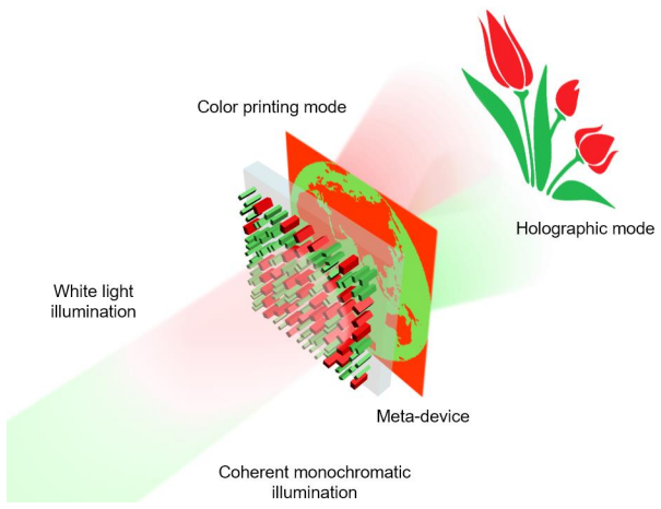
Pith's one-line read One flat silicon surface can print a color image under white light and project two different holograms under red and green lasers.
desk verdict A first demonstration of single-layer color printing plus two wavelength-multiplexed holograms; the independence claim overreaches but the experiment is solid and worth reviewing. read the letter →
The pith
A machine-rendered reading of the paper's core claim, the machinery that carries it, and where it could break.
The reading
What carries the argument
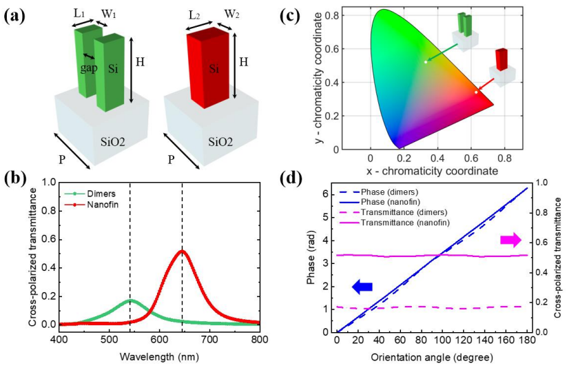
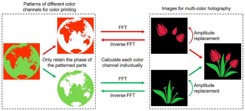
The central object is the pairing of a spectral filter and a geometric phase inside one subwavelength pixel: an amorphous-silicon dimer (length 90 nm, width 50 nm, gap 80 nm) and a nanofin (length 125 nm, width 90 nm), both 300 nm tall in a 300 nm lattice. Each shape's cross-polarized transmission spectrum makes it an amplitude filter for one hologram wavelength, while its in-plane rotation angle $\varphi$ imparts a Pancharatnam-Berry phase $\Phi = 2\sigma\varphi$ to circularly polarized light of helicity $\sigma$ without changing that spectrum. The modified parallel Gerchberg-Saxton algorithm is what allows the sub-holograms to be computed over irregular, color-pattern-shaped regions rather than simple rectangles, keeping the holographic channels bound to the visible color layout.
What would settle it
Repeatedly measure the cross-polarized transmission spectrum of a fabricated dimer and nanofin while their orientation angles are rotated from 0 degrees to 180 degrees, and then illuminate the full device with a tunable laser in 5 nm steps; if the transmission spectra shift with orientation or if the unwanted hologram appears with comparable intensity inside the 540 nm or 645 nm design bands, the claimed spectral-spatial independence is not realized.
Extended reading notes
Core claim
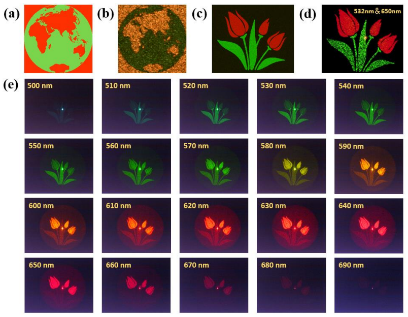
The authors experimentally demonstrate a single-layer all-dielectric metasurface that functions as both a color print and a wavelength-multiplexed hologram. The device, made of amorphous-silicon dimers and nanofins on glass, shows a bicolor earth map under white light, and when illuminated with red and green lasers it reconstructs the images 'red blossoms' and 'green leaves' in the Fourier plane. The spectral response is set by geometry: dimers transmit around 20% cross-polarized light at 540 nm and nanofins around 50% at 645 nm, with simulated crosstalk below 5%. The spatial phase is set independently by the azimuthal angle of each meta-atom, giving the full 0 to 2π Pancharatnam-Berry phase. A modified parallel Gerchberg-Saxton algorithm divides the aperture along the color-pattern boundaries and computes phase-only sub-holograms matched to each region, so the holograms are readable in the same pixels that form the color print.
Load-bearing premise
The design hinges on the idea that rotating a meta-atom changes only its phase, not its color filter, so the color image and the holograms can be set pixel by pixel without disturbing each other.
Editorial extensions
If this is right
- The two-color scheme can be extended to three or more spectral channels by choosing low-absorption materials and additional meta-atom geometries, as the authors suggest with titanium dioxide and silicon nitride.
- A single device can display an overt authentication image in white light while concealing independent laser-readable holograms, making counterfeiting harder because both spectral and phase responses must be reproduced.
- Changing the illumination wavelength switches the holographic output without moving or reconfiguring the device, so the same surface works as a compact wavelength-selective projector.
- Phase and color are both defined at the pixel level, so the extra information does not cost extra device area or require multilayer alignment.
Reading between the lines
- The paper uses only one circular polarization handedness; because flipping the handedness reverses the sign of every Pancharatnam-Berry phase, the same surface could in principle record two additional polarization-selected holograms without changing the color print.
- The authors report both holograms appearing between 550 and 630 nm, so the practical channel spacing is set by the spectral tails of the two filters; a systematic sweep of wavelength separation against measured crosstalk would map how many channels a single metasurface can realistically hold.
- Near-field coupling between neighboring dimer and nanofin pixels at the boundaries of the color pattern is not separately studied; comparing isolated atoms with atoms embedded in the actual pattern would show whether printed colors shift near region edges and whether hologram efficiency is position-dependent.
Signed reviews
Editorial analysis
A structured set of objections, weighed in public.
Referee Report
Summary. The manuscript reports a single-layer all-dielectric silicon metasurface that combines structural color printing under white-light illumination with two wavelength-multiplexed holograms reconstructed under red and green laser illumination. The design uses two types of amorphous-silicon meta-atoms (dimers and nanofins) that act as mutually exclusive spectral filters at the two design wavelengths, while the in-plane orientation of each meta-atom encodes Pancharatnam-Berry phase for the holographic mode. A modified parallel Gerchberg-Saxton algorithm is introduced to generate sub-holograms matched to arbitrary color-pattern regions. Two fabricated samples are characterized: one shows a bicolor earth map and reconstructs 'red blossoms' and 'green leaves' holograms; the second shows a QR-code color print and two text holograms. The authors claim that the spectral and spatial responses are modulated simultaneously and independently at the subwavelength scale.
Significance. If the claims are fully supported, the work provides a compelling single-layer platform for combining color printing and wavelength-multiplexed holography, with direct relevance to optical security, anti-counterfeiting, and information storage. The main strengths are the experimental realization of both modes on the same device, the use of CMOS-compatible amorphous silicon, and the proposed modified GS algorithm, which allows hologram regions to follow arbitrary color-print patterns. The paper also includes a broadband characterization showing wavelength-dependent hologram switching, which is an informative addition. However, the quantitative characterization is thin in several respects, and a key decoupling assumption is validated only for periodic, identically oriented unit cells, not for the actual aperiodic mixed-orientation layout.
major comments (3)
- [Design principle, Fig. 2(d)] The claim that spectral and spatial responses are 'totally independent' rests on the FDTD result that the cross-polarized transmittance is uniform versus orientation angle for dimers and nanofins. This calculation is performed for periodic arrays with a single identical orientation per simulation. In the actual device, the two meta-atom types are intermixed at a 300 nm pitch with per-pixel orientation angles that vary randomly. In such a dense aperiodic environment, near-field coupling between neighboring meta-atoms can make the spectral response orientation-dependent, which would couple the hologram encoding to the color printing. The paper does not provide supercell simulations, a fabricated control with aligned versus encoded orientations, or any direct measurement of the orientation dependence of the spectral response in the mixed layout. This is a load-bearing assumption for the central claim of independence, and it needs to be addressed explicitly, either with additional simulations/experiments or by tempering the 'totally independent' claim to what the data actually support.
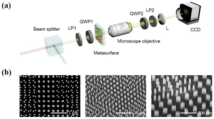
- [Experimental results, Fig. 5(e)] The wavelength-scan data show that both holographic images are reconstructed simultaneously over the range 550-630 nm, meaning the two meta-atom types do not act as clean mutually exclusive spectral filters in the fabricated device. The paper attributes this to non-zero transmittance of the two filters, but it provides no measured cross-polarized transmittance spectra of the fabricated dimers and nanofins and no quantitative metric for crosstalk or image contrast. Without such numbers, the statement that the holograms are 'crosstalk-free' at the intended wavelengths (made for the second sample) is not substantiated. The authors should report the measured spectral selectivity of the fabricated meta-atoms and define a quantitative crosstalk/contrast ratio for the reconstructed holograms, rather than relying on visual inspection.
- [Experimental results, Fig. 5(b) and Discussion] The color printing demonstration is only qualitative. The simulated CIE coordinates in Fig. 2(c) are not compared with measured color coordinates, and the paper notes that the experimental color of the dimers (dark green versus designed green) deviates from simulation but gives no quantitative colorimetric analysis. Because the dual-mode claim depends on the spectral response being preserved in the final fabricated device, the authors should provide measured reflection/transmission spectra or measured CIE coordinates of the actual printed regions, along with an estimate of fabrication-induced color shift. This would strengthen the evidence that the spectral channel survives in the integrated device.
minor comments (5)
- [Figure 5(d) caption] The caption states 'red (532 nm) and green (650 nm) laser beams,' which is inconsistent with the standard association that 532 nm is green and 650 nm is red. Please correct the wavelengths or the color labels.
- [Calculation of the computer-generated hologram] The feedback function Tn = T + |T - Tn'|κ is introduced without specifying how the value of κ is chosen or how convergence of the GS algorithm is assessed. Please provide the chosen κ, the number of iterations, and a representative convergence plot or error metric.
- [Experimental results] The claim that the holographic images are reconstructed with 'high resolution and matched magnifications' is not supported by quantitative measures such as angular field of view, signal-to-noise ratio, or diffraction efficiency. Please provide these numbers or soften the claim.
- [Discussion] The phrase 'the spectral response is totally independent of the spatial response' is stronger than what the data show given the observed wavelength crosstalk. Consider replacing 'totally' with a more qualified wording such as 'largely independent under the designed operating conditions.'
- [Methods] The RCWA optimization sweep is described briefly; please specify the step sizes for the parameter sweeps of L, W, and gap, and whether the optimization used a figure of merit based on the cross-polarized transmittance at the two design wavelengths.
Circularity Check
No circularity: the paper is a self-contained construction whose spectral responses are simulated independently, whose hologram targets are external inputs, and whose only self-citations are non-load-bearing.
full rationale
The paper's chain is a design-and-demonstrate workflow rather than a derivation: two meta-atom geometries are selected by RCWA simulations of cross-polarized transmittance (Fig. 2b); FDTD is used to check that rotating each geometry for Pancharatnam-Berry phase leaves transmittance uniform (Fig. 2d); the surface is partitioned according to a chosen color pattern; a parallel Gerchberg-Saxton algorithm is run with the desired holographic target images as external inputs to obtain orientation-only phase profiles; and the fabricated samples are measured. No quantity that is predicted is also used to define the input. The two meta-atom types are characterized by independent spectral simulations, not fitted to the final holograms or color prints. The feedback formula cited to the authors' prior work [24] is stated explicitly in the text and only accelerates convergence; it is not load-bearing for the existence or independence of the multiplexed holograms. The paraxial scaling relation λ1 z1 = λ2 z2 from [45] is standard optics. The claim that the spectral and spatial responses are 'totally independent' is supported by the color-region indexing and by FDTD checks, and the observed 550-630 nm crosstalk is reported as an experimental fidelity limitation rather than used as an input. There is no self-definitional reduction, fitted input renamed as prediction, or uniqueness argument imported from the authors' prior work. The paper is therefore judged non-circular, with minor self-citations that do not raise the circularity score.
Assumptions & free parameters
free parameters (5)
- Dimer geometry (L1, W1, gap) =
90 nm, 50 nm, 80 nm
- Nanofin geometry (L2, W2) =
125 nm, 90 nm
- Design heights and period =
H=300 nm, P=300 nm
- Design wavelengths =
540 nm and 645 nm
- Feedback parameter kappa =
not specified
assumptions (4)
- standard math PB phase relation Phi = 2*sigma*phi
- domain assumption RCWA and FDTD simulation accuracy
- domain assumption Measured a-Si refractive index by ellipsometry
- standard math Paraxial scaling lambda1*z1 = lambda2*z2
Cite this review
Pith. "Pith review of Simultaneous spectral and spatial modulation for color printing and holography using all-dielectric metasurfaces." pith.science (2026). https://pith.science/paper/E4NDLDYT
@misc{pith2026190808899,
  author       = {Pith},
  title        = {Pith review of: Simultaneous spectral and spatial modulation for color printing and holography using all-dielectric metasurfaces},
  year         = {2026},
  howpublished = {\url{https://pith.science/paper/E4NDLDYT}},
  note         = {Machine review of arXiv:1908.08899}
}
read the original abstract
Metasurfaces possess the outstanding ability to tailor phase, amplitude and even spectral responses of light with an unprecedented ultrahigh resolution, thus have attracted significant interests. Here, we propose and experimentally demonstrate a novel meta-device that integrates color printing and computer-generated holograms within a single-layer dielectric metasurface by modulating spectral and spatial responses at subwavelength scale, simultaneously. In our design, such metasurface appears as a microscopic color image under white light illumination, while encrypting two different holographic images that can be projected at the far-field when illuminated with red and green laser beams. We choose amorphous silicon dimers and nanofins as building components and use a modified parallel Gerchberg-Saxton algorithm to obtain multiple sub-holograms with arbitrary spatial shapes for image-indexed arrangements. Such a method can further extend the design freedom of metasurfaces. By exploiting spectral and spatial control at the level of individual pixels, multiple sets of independent information can be introduced into a single-layer device, the additional complexity and enlarged information capacity are promising for novel applications such as information security and anti-counterfeiting.
Figures
Figures from the paper (2 more)
Reference graph
Works this paper leans on
-
[1]
School of Optics and Photonics, Beijing Institute of Technology, Beijing, 100081, China
-
[2]
Department of Physics, University of Paderborn, Warburger Straße 100, 33098 Paderborn, Germany
-
[3]
Laser Micro/Nano-Fabrication Laboratory, School of Mechanical Engineering, Beijing Institute of Technology, Beijing 100081, China Abstract:Metasurfaces possess the outstanding ability to tailor phase, amplitude and even spectral response s of light with an unprecedented ultrahigh resolution, thus have attracted significant interest s. Here, we propose and...
work page 1931
-
[4]
N. Yu, F. Capasso, Nat. Mater. 2014, 13, 139
work page 2014
-
[5]
Y. Chen, X. Yang, J. Gao, Light: Sci. Appl. 2018, 7, 1
work page 2018
-
[6]
D. Lin, P. Fan, E. Hasman, M. L. Brongersma, Science 2014, 345, 298
work page 2014
- [7]
-
[8]
P. Genevet, F. Capasso, F. Aieta, M. Khorasaninejad, R. Devlin, Optica 2017, 4, 139
work page 2017
Show all 51 references
-
[9]
M. Pu, X. Ma, X. Li, Y. Guo, X. Luo, J. Mater. Chem. C 2017, 5, 4361
2017
-
[10]
Y. Yang, W. Wang, P. Moitra, I. I. Kravchenko, D. P. Briggs, J. Valentine, Nano Lett. 2014, 14, 1394
2014
-
[11]
Huang, H
K. Huang, H. Liu, S. Restuccia, M. Q. Mehmood, S. Mei, D. Giovannini, A. Danner, M. J. Padgett, J. Teng, C. Qiu, Light: Sci. Appl. 2018, 7, 17156
2018
-
[12]
Y. Chen, X. Yang, J. Gao, Adv. Opt. Mater. 2018, 6, 1800646
2018
-
[13]
Arbabi, Y
A. Arbabi, Y. Horie, A. J. Ball, M. Bagheri, A. Faraon, Nat. Commun. 2015, 6, 7069
2015
-
[14]
S. Wang, P. C. Wu, V. Su, Y. Lai, C. H. Chu, J. Chen, S. Lu, J. Chen, B. Xu, C. Kuan, T. Li, S. Zhu, D. P. Tsai, Nat. Commun. 2017, 8, 187
2017
-
[15]
S. Wang, P. C. Wu, V. Su, Y. Lai, M. Chen, H. Y. Kuo, B. H. Chen, Y. H. Chen, T. Huang, J. Wang, R. Lin, C. Kuan, T. Li, Z. Wang, S. Zhu, D. P. Tsai, Nat. Nanotechnol. 2018, 13, 227
2018
-
[16]
W. T. Chen, A. Y. Zhu, V. Sanjeev, M. Khorasaninejad, Z. Shi, E. Lee, F. Capasso, Nat. Nanotechnol. 2018, 13, 220
2018
-
[17]
X. Ni, Z. J. Wong, M. Mrejen, Y. Wang, X. Zhang, Science 2015, 349, 1310
2015
-
[18]
N. C. Pegard, J. W. Fleischer, Opt. Lett. 2011, 36, 2551
2011
-
[19]
X. M. Goh, Y. Zheng, S. J. Tan, L. Zhang, K. Kumar, C. Qiu, J. K. W. Yang, Nat. Commun. 2014, 5, 5361
2014
-
[20]
L. Jin, Z. Dong, S. Mei, Y. F. Yu, Z. Wei, Z. Pan, S. D. Rezaei, X. Li, A. I. Kuznetsov, Y. S. Kivshar, J. K. W. Yang, C. Qiu, Nano Lett. 2018, 18, 8016
2018
-
[21]
R. Zhao, B. Sain, Q. Wei, C. Tang, X. Li, T. Weiss, L. Huang, Y. Wang, T. Zentgraf, Light: Sci. Appl. 2018, 7, 95
2018
-
[22]
H. Liu, B. Yang, Q. Guo, J. Shi, C. Guan, G. Zheng, H. Muehlenbernd, G. Li, T. Zentgraf, S. Zhang, Sci. Adv. 2017, 3, e1701477
2017
-
[23]
W. Ye, F. Zeuner, X. Li, B. Reineke, S. He, C. Qiu, J. Liu, Y. Wang, S. Zhang, T. Zentgraf, Nat. Commun. 2016, 7, 11930
2016
-
[24]
Z. Deng, J. Deng, X. Zhuang, S. Wang, K. Li, Y. Wang, Y. Chi, X. Ye, J. Xu, G. P. Wang, R. Zhao, X. Wang, Y. Cao, X. Cheng, G. Li, X. Li, Nano Lett. 2018, 18, 2885
2018
-
[25]
Zheng, H
G. Zheng, H. Muehlenbernd, M. Kenney, G. Li, T. Zentgraf, S. Zhang, Nat. Nanotechnol. 2015, 10, 308
2015
-
[26]
Genevet, F
P. Genevet, F. Capasso, Rep. Prog. Phys. 2015, 78, 024401
2015
-
[27]
Q. Wei, L. Huang, X. Li, J. Liu, Y. Wang, Adv. Opt. Mater. 2017, 5, 1700434
2017
-
[28]
S. M. Kamali, E. Arbabi, A. Arbabi, Y. Horie, M. Faraji -Dana, A. Faraon, Phys. Rev. X 2017, 7, 041056
2017
-
[29]
Y. Chen, X. Yang, J. Gao, Light: Sci. Appl. 2018, 7, 84
2018
-
[30]
W. Zhao, B. Liu, H. Jiang, J. Song, Y. Pei, Y. Jiang, Opt. Lett. 2016, 41, 147
2016
-
[31]
F. Dong, H. Feng, L. Xu, B. Wang, Z. Song, X. Zhang, L. Yan, X. Li, Y. Tian, W. Wang, L. Sun, Y. Li, W. Chu, ACS Photonics 2019, 6, 230
2019
-
[32]
B. Wang, F. Dong, D. Yang, Z. Song, L. Xu, W. Chu, Q. Gong, Y. Li, Optica 2017, 4, 1368
2017
-
[33]
B. Wang, F. Dong, Q. Li, D. Yang, C. Sun, J. Chen, Z. Song, L. Xu, W. Chu, Y. Xiao, Q. Gong, Y. Li, Nano Lett. 2016, 16, 5235
2016
-
[34]
L. Wang, S. Kruk, H. Tang, T. Li, I. Kravchenko, D. N. Neshev, Y. S. Kivshar, Optica 2016, 3, 1504
2016
-
[35]
K. E. Chong, I. Staude, A. James, J. Dominguez, S. Liu, S. Campione, G. S. Subramania, T. S. Luk, M. Decker, D. N. Neshev, I. Brener, Y. S. Kivshar, Nano Lett. 2015, 15, 5369
2015
-
[36]
K. E. Chong, L. Wang, I. Staude, A. R. James, J. Dominguez, S. Liu, G. S. Subramania, M. Decker, D. N. Neshev, I. Brener, Y. S. Kiyshar, ACS Photonics 2016, 3, 514
2016
-
[37]
Z. Yang, R. Jiang, X. Zhuo, Y. Xie, J. Wang, H. Lin, Phys. Rep. 2017, 701, 1
2017
-
[38]
S. Yuan, X. Qiu, C. Cui, L. Zhu, Y. Wang, Y. Li, J. Song, Q. Huang, J. Xia, ACS Nano 2017, 11, 10704
2017
-
[39]
Zhang, M
F. Zhang, M. Pu, X. Li, P. Gao, X. Ma, J. Luo, H. Yu, X. Luo, Adv. Funct. Mater. 2017, 27, 1704295
2017
-
[40]
Z. Ma, Y. Li, Y. Li, Y. Gong, S. A. Maier, M. Hong, Opt. Express 2018, 26, 6067
2018
-
[41]
Kumar, H
K. Kumar, H. Duan, R. S. Hegde, S. C. W. Koh, J. N. Wei, J. K. W. Yang, Nat. Nanotechnol. 2012, 7, 557
2012
-
[42]
S. J. Tan, L. Zhang, D. Zhu, X. M. Goh, Y. M. Wang, K. Kumar, C. Qiu, J. K. W. Yang, Nano Lett. 2014, 14, 4023
2014
-
[43]
J. S. Clausen, E. Hojlund-Nielsen, A. B. Christiansen, S. Yazdi, M. Grajower, H. Taha, U. Levy, A. Kristensen, N. A. Mortensen, Nano Lett. 2014, 14, 4499
2014
-
[44]
X. Zang, F. Dong, F. Yue, C. Zhang, L. Xu, Z. Song, M. Chen, P. Chen, G. S. Buller, Y. Zhu, S. Zhuang, W. Chu, S. Zhang, X. Chen, Adv. Mater. 2018, 30, 1707499
2018
-
[45]
Z. Li, A. W. Clark, J. M. Cooper, ACS Nano 2016, 10, 492
2016
-
[46]
Nagasaki, M
Y. Nagasaki, M. Suzuki, J. Takahara, Nano Lett. 2017, 17, 7500
2017
-
[47]
X. Duan, S. Kamin, N. Liu, Nat. Commun. 2017, 8, 14606
2017
-
[48]
Huang, X
L. Huang, X. Chen, H. Muehlenbernd, H. Zhang, S. Chen, B. Bai, Q. Tan, G. Jin, K. Cheah, C. Qiu, J. Li, T. Zentgraf, S. Zhang, Nat. Commun. 2013, 4, 2808
2013
-
[49]
K. T. P. Lim, H. Liu, Y. Liu, J. K. W. Yang, Nat. Commun. 2019, 10, 25
2019
-
[50]
G. Yoon, D. Lee, K. T. Nam, J. Rho, ACS Nano 2018, 12, 6421
2018
-
[51]
Zhang, L
Y. Zhang, L. Shi, D. Hu, S. Chen, S. Xie, Y. Lu, Y. Cao, Z. Zhu, L. Jin, B. Guan, S. Rogge, X. Li, Nanoscale Horiz. 2019, 4, 601
2019
Reviewed August 14, 2026 · model on record in the stance chip above.
Discussion (0). Continue with ORCID to comment.