REVIEW 3 major objections 6 minor 79 references
Aharonov-Bohm interferences in polycrystalline graphene
T0 review · 3 major / 6 minor · reviewed 2026-08-14 · deepseek-v4-flash
Pith's one-line read Grain-boundary scattering can couple quantum Hall edge states and produce Aharonov-Bohm oscillations in polycrystalline graphene.
desk verdict The circulating-orbit picture is well supported, but the 'h/eS' period check fits the area rather than predicting it, so the AB identification is underdetermined. read the letter →
The pith
A machine-rendered reading of the paper's core claim, the machinery that carries it, and where it could break.
The reading
What carries the argument
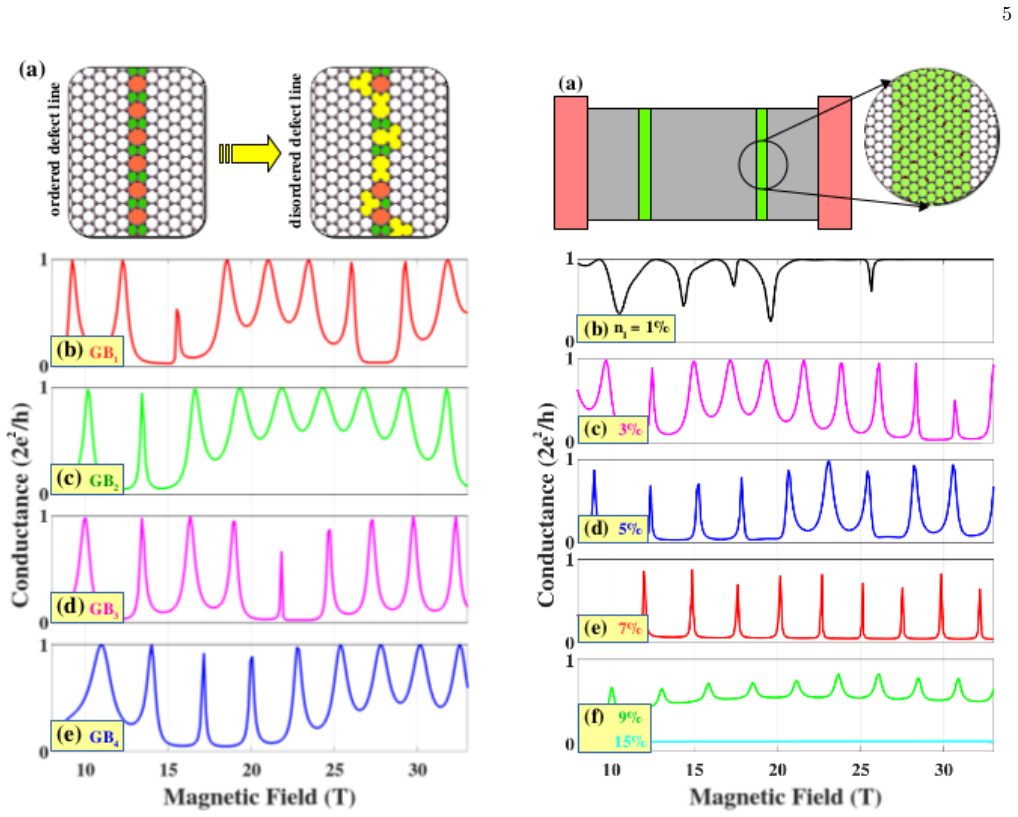
The central mechanism is the defect line as a partial scatterer that couples quantum Hall edge states. Under a strong perpendicular field, an electron following a cyclotron orbit near a grain boundary is split by scattering into a reflected and a transmitted branch, so the two sides of the line carry opposite skipping orbits; with two parallel defect lines, the branches meet and enclose a circulating channel inside the middle grain. The Aharonov-Bohm phase accumulated on that channel, $eBS/\hbar$ for enclosed area $S$, makes the conductance oscillate with field period $\Delta B = h/eS$. Computationally, the argument rests on a $p_z$ tight-binding Hamiltonian with Peierls phases, relaxed atomic structures from classical molecular dynamics, Landauer transport via Green's functions, and an on-site-energy model for oxygen impurities fitted to DFT band structure.
What would settle it
Measure the two-terminal conductance of a gated two-grain-boundary graphene device at low temperature while sweeping the perpendicular magnetic field; the claim predicts periodic oscillations with period $\Delta B = h/eS$. The absence of such oscillations, or a period inconsistent with the circulating area measured by a local probe, would falsify the central claim.
Extended reading notes
Core claim
The paper's central claim is that defect scattering—usually treated as a nuisance—can create the transmission paths between quantum Hall edge states that Aharonov-Bohm interferometers require. In a single grain boundary, electrons following cyclotron orbits are partly reflected and partly transmitted across the defect line, so the two sides carry opposite skipping orbits; with two parallel grain boundaries, this couples the edge channels so that electrons in the middle grain circulate around its enclosed area. The accumulated Aharonov-Bohm phase makes the conductance an oscillating function of magnetic field, with peaks and valleys that correspond to constructive and destructive interference. The oscillations obey the standard period $\Delta B = h/eS$ with the circulating area about 20% smaller than the geometric grain area, are strongest below the first Landau level, and persist when the boundaries are disordered with realistic vacancy densities. The identical physics is reproduced in ribbons where the two barriers are made of oxygen impurities rather than structural defects.
Load-bearing premise
The whole effect depends on electrons keeping a stable quantum phase while being scattered by the defect lines and circulating inside the internal grain; any real decoherence between those events would blur or destroy the oscillations.
Editorial extensions
If this is right
- A two-grain-boundary graphene ribbon becomes a magnetic-field-tunable interferometer whose oscillation period directly measures the area of the circulating channel, not the geometric grain area (about 20% smaller here).
- The predicted oscillations survive edge roughness and boundary disorder, with strong interference still claimed at vacancy densities up to about 10%, because the underlying quantum Hall edge states are themselves stable under such scatterers.
- The mechanism does not rely on bipolar doping, so it extends to unipolar graphene and, in principle, to other two-dimensional materials and lateral heterostructures.
- Two narrow oxygen-impurity barriers reproduce the same conductance oscillations at impurity densities of roughly 3% to 7%, offering a chemically patterned alternative to structural grain boundaries.
Reading between the lines
- If the effect holds in experiment, the same geometry could serve as a sensitive magnetometer or as a local probe of grain area and edge structure, since the AB period encodes the enclosed area directly.
- The model is single-particle and phase-coherent; a natural extension is to test whether interaction-induced fractional quantum Hall states inside the grain modify or sharpen the interference pattern.
- The oxygen-barrier result suggests that standard oxidation and reduction lithography could fabricate such interferometers without needing atomically precise defect lines, which would make the proposal easier to test.
- Because decoherence is not modeled, measuring the temperature dependence of the oscillation visibility would reveal the phase coherence length of the circulating channel, a quantity the paper leaves unestimated.
Signed reviews
Editorial analysis
A structured set of objections, weighed in public.
Referee Report
Summary. The manuscript proposes that defect scattering at graphene grain boundaries can provide tunneling paths between quantum Hall edge states, so that a polycrystalline graphene sample containing two parallel grain boundaries acts as an Aharonov-Bohm (AB) interferometer. The authors use an atomistic pz tight-binding Hamiltonian with Peierls phases and a Green's function/Landauer transport formalism to compute conductance oscillations as a function of magnetic field. They present LDOS maps showing circulating electron trajectories inside the internal grain, claim that the oscillation period satisfies the standard AB formula ΔB = h/eS with an effective area S smaller than the geometric grain area, and extend the same mechanism to graphene ribbons with two oxygen-impurity barriers. They further claim robustness to edge disorder and to grain-boundary vacancy disorder up to about 10% vacancy density.
Significance. If the interpretation holds, the work offers a new route to AB interferometers in the quantum Hall regime that exploits the unavoidable defects of polycrystalline graphene, and it is plausibly extendable to other 2D materials. The manuscript has clear strengths: the atomistic models include relaxed grain-boundary structures and realistic disorder, the LDOS panels provide visual evidence of circulating trajectories, the disorder study covers many independent configurations, and the impurity model is explicitly calibrated to DFT bandstructure. The main weakness is that the quantitative AB-period evidence is partly circular, because the effective area S is inferred from the oscillations it is supposed to explain, and the alternative explanation in terms of skipping-orbit/cavity resonances suggested by the single-grain-boundary results in the Supplementary Information is not excluded. The central physical picture may be correct, but the specific identification of the observed modulations as AB interference requires additional tests.
major comments (3)
- [Sec. III, Fig. 3] The claim that the conductance oscillations follow the AB period formula ΔB = h/eS is tested using effective areas S ≈ 1750 nm² and 3490 nm² that are inferred from the very same oscillations, with the same 20% reduction from the geometric area used for both LD values. This makes the agreement a fit rather than a parameter-free test. To make the AB identification load-bearing, the authors should determine S independently, for example from the LDOS circulating trajectories or by explicitly varying the ribbon width W at fixed LD and showing that the period scales as 1/S with S derived from geometry.
- [Supplementary Sec. 1; Sec. III] The Supplementary Information shows that a single grain boundary already produces magneto-conductance oscillations from skipping orbits, with the period controlled by the ratio of the cyclotron radius to the defect-line length. For the two-boundary systems, the period roughly doubles when LD doubles from 44 nm to 88 nm, which is also naturally expected for a two-boundary skipping-orbit or cavity resonance whose frequency is set by the cavity length, rather than uniquely by an enclosed-area AB phase. The authors should explicitly rule out this alternative, for example by showing the dependence of the oscillation frequency on W at fixed LD, and by comparing the observed frequencies with a cavity-resonance model.
- [Sec. III, paragraph following Fig. 4] The robustness claim is not fully supported by the presented data: the text asserts that strong AB oscillations persist 'up to about 10%' vacancy density, but the data shown in the Supplementary Information only cover up to 6%, and edge-disorder results are stated to be 'not further presented' although the conclusion claims robustness to disorder. The authors should either provide the 10% data and the edge-disorder results, or qualify the robustness statement to the parameter range actually computed.
minor comments (6)
- [Throughout] There are typographical errors such as 'hoping energies' for 'hopping energies', and the onsite impurity energy is written as εon in the main text but as eon in the Supplementary Information; please unify the notation.
- [Sec. III, Fig. 3] The procedure for extracting the effective area S from the LDOS or from the oscillation period is not described; please specify how the circulating-channel area is defined and measured.
- [Sec. II; Eq. (1)] The gauge used for the Peierls phase φnm is not specified; please state the Landau gauge and the boundary conditions employed in the Green's function transport calculations.
- [Sec. III, experimental outlook] The calculations are zero-temperature coherent single-particle transport with no dephasing or temperature effects; since the experimental relevance of oscillations at a few teslas depends on phase coherence, a short discussion or estimate of the relevant coherence scales would strengthen the paper.
- [References] Reference [56] is cited as 'in preparation'; if it is not yet available, it should either be updated or removed, since the reader cannot verify the claimed demonstration of ballistic transport along grain boundaries.
- [Supplementary Fig. S7] The caption refers to 'V- and P-points' without defining these labels; please clarify whether they denote valley and peak positions or something else.
Circularity Check
AB period check relies on a fitted effective area; the central LDOS circulation result is independent but the quantitative h/eS validation is partly circular.
-
fitted input called prediction
[Sec. III, paragraph discussing Fig. 3 (main text)]
"First, the period of these AB oscillations is shown to satisfy very well the standard formula ∆B = h/eS where S is determined as the surface area enclosed by circulating channels inside the internal graphene grain. ... In particular, the above formula accurately estimates the period of conductance oscillations in Figs.3.a-b using S≃ 1750 nm 2 (for LD≃ 44 nm) and 3490 nm 2 (LD≃ 88 nm), which are about 20% smaller than the values 2200 nm 2 and 4400 nm2 of the area of the internal grain, respectively."
The effective area S is not independently measured or predicted; it is assigned as 0.795 times the geometric grain area for both LD values. Since any periodic conductance modulation has a period, choosing S so that h/eS matches the observed period makes the 'agreement' with the AB formula tautological. The only non-tautological content is the approximate doubling of S with LD, but the uniform 20% reduction factor is a single fitted parameter. Thus the claim that the oscillations obey the AB period h/eS is partly a restatement of the fitted input rather than an independent prediction.
full rationale
The paper's main computational content — atomistic tight-binding Green's function transport through polycrystalline graphene with two grain boundaries — is self-contained and not circular. The circulating LDOS patterns in Fig. 2 and the robustness of conductance oscillations against edge and grain-boundary disorder are genuine numerical results, not derived from the conclusion. However, the quantitative identification of the oscillations as Aharonov-Bohm with period ΔB = h/eS is weakened by the way S is handled. The text states that the period is 'accurately estimated' using S ≈ 1750 nm² and 3490 nm², both about 20% smaller than the geometric grain areas. No independent, LDOS-based measurement of the enclosed circulating area is shown for the idealized ribbons of Fig. 3; the 20% reduction factor is effectively a single fitted parameter applied to both systems. Consequently, the claimed agreement with the AB formula is partly by construction, which places this step in the 'fitted input called prediction' category. The approximate scaling of S with LD does provide some independent content, preventing a higher score. The self-citations to the authors' prior works (refs. 33 and 56) are not load-bearing for the central claim. The single-grain-boundary skipping-orbit oscillations demonstrated in the Supplementary Information raise an alternative explanation for the conductance modulations, but that is an underdetermination concern rather than a circularity, so it is not counted in the score.
Assumptions & free parameters
free parameters (2)
- Effective enclosed area S in AB period formula =
1750 nm2 and 3490 nm2 for LD=44 nm and 88 nm
- Oxygen impurity onsite energy epsilon_on =
28 eV
assumptions (5)
- domain assumption The pz nearest-neighbor tight-binding Hamiltonian with Peierls phases and strain-modified hoppings captures low-energy magnetotransport in polycrystalline graphene.
- standard math The Landauer-Buttiker formula and Green's function technique give the conductance of the open system.
- domain assumption Grain boundaries can be represented by ordered pentagon/heptagon defect lines with randomly added vacancies at densities of 2 to 6 percent.
- domain assumption Electron transport is fully phase coherent at the Fermi energies considered.
- domain assumption DFT calculations with OpenMX provide a reliable reference for the oxygen-impurity bandstructure.
Cite this review
Pith. "Pith review of Aharonov-Bohm interferences in polycrystalline graphene." pith.science (2026). https://pith.science/paper/IKTZCWVF
@misc{pith2026190809399,
  author       = {Pith},
  title        = {Pith review of: Aharonov-Bohm interferences in polycrystalline graphene},
  year         = {2026},
  howpublished = {\url{https://pith.science/paper/IKTZCWVF}},
  note         = {Machine review of arXiv:1908.09399}
}
read the original abstract
Aharonov-Bohm (AB) interferences in the quantum Hall regime can be achieved, provided that electrons are able to transmit between two edge channels in nanostructures. Pioneering approaches include quantum point contacts in 2DEG systems, bipolar graphene p-n junctions, and magnetic field heterostructures. In this work, defect scattering is proposed as an alternative mechanism to achieve AB interferences in polycrystalline graphene. Indeed, due to such scattering, the extended defects across the sample can act as tunneling paths connecting quantum Hall edge channels. Consequently, strong AB oscillations in the conductance are predicted in polycrystalline graphene systems with two parallel grain boundaries. In addition, this general approach is demonstrated to be applicable to nano-systems containing two graphene barriers with functional impurities and perspectively, can also be extended to similar systems of 2D materials beyond graphene.
Figures


Figures from the paper (2 more)

Reference graph
Works this paper leans on
-
[1]
A. C. Ferrari et al., Nanoscale 7, 4598-4810 (2015). [2] P. T. Araujoa, M. Terrones, and M. S. Dresselhaus, 7 Mater. Today 15, 98-109 (2012)
work page 2015
-
[2]
Graphene grains and grain boundaries investigated in Fig. 2 of the main text Fig.S3 presents a zoom of the atomic structure of the system investigated in Fig.2 of the main text. Even though the grains 1 and 3 are formed by the same graphene lattice (for simplicity), it represents three main structural properties, which can be practically obtained as in re...
-
[3]
D. Chen, H. Feng, and J. Li, Chem. Rev. 112, 6027-6053 (2012)
work page 2012
- [4]
-
[5]
O. V. Yazyev and Y. P. Chen, Nat. Nanotechnol. 9, 755- 767 (2014)
work page 2014
-
[6]
A. W. Cummings et al. , Adv. Mater. 26, 5079-5094 (2014)
work page 2014
- [7]
- [8]
Show all 79 references
-
[9]
D. V. Tuan, J. Kotakoski, T. Louvet, F. Ortmann, J. C. Meyer, and S. Roche, Nano Lett. 13, 1730-1735 (2013)
2013
-
[10]
O. V. Yazyev and S. G. Louie, Nat. Mater. 9, 806-809 (2010)
2010
-
[11]
Dechamps, V
S. Dechamps, V. Hung Nguyen, and J.-C. Charlier, Nanoscale 10, 7759-7768 (2018)
2018
-
[13]
Hung Nguyen, T
V. Hung Nguyen, T. X. Hoang, P. Dollfus and J.-C. Char- lier, Nanoscale 8, 11658-11673 (2016)
2016
-
[14]
Gunlycke and C
D. Gunlycke and C. T. White, Phys. Rev. Lett. 106, 136806 (2011)
2011
-
[15]
Hung Nguyen, S
V. Hung Nguyen, S. Dechamps, P. Dollfus, and J.-C. Charlier, Phys. Rev. Lett. 117, 247702 (2016)
2016
-
[16]
Lahiri, Y
J. Lahiri, Y. Lin, P. Bozkurt, I. I. Oleynik, M, Batzill, Nat. Nanotechnol. 5, 326-329 (2010)
2010
-
[17]
Ma et al., Phys
C. Ma et al., Phys. Rev. Lett. 112, 226802 (2014)
2014
-
[18]
G. I. Mark, P. Vancso, P. H. Lambin, C. Hwang, and L. P. Biro, J. Nanophotonics 6, 061718 (2012)
2012
-
[20]
B. Yang, H. Xu, J. Lu, and K. P. Loh, J. Am. Chem. Soc. 136, 12041 (2014)
2014
-
[21]
Aharonov and D
Y. Aharonov and D. Bohm, Phys. Rev. 115, 485-491 (1959)
1959
-
[22]
C. P. Search, J. R. E. Toland, and M. Zivkovic, Phys. Rev. A 79, 053607 (2009)
2009
-
[23]
Brassard, I
G. Brassard, I. Chuang, S. Lloyd, and C. Monroe, PNAS 95, 11032-11033 (1998)
1998
-
[24]
L. P. L´ evy, G. Dolan, J. Dunsmuir, and H. Bouchiat, Phys. Rev. Lett. 64, 2074 (1990)
1990
-
[25]
Mailly, C
D. Mailly, C. Chapelier, and A. Benoit, Phys. Rev. Lett. 70, 2020 (1993)
1993
-
[26]
C. de C. Chamon, D. E. Freed, S. A. Kivelson, S. L. Sondhi, and X. G. Wen, Phys. Rev. B 55, 2331 (1997)
1997
-
[27]
F. E. Camino, Wei Zhou, and V. J. Goldman, Phys. Rev. Lett. 98, 076805 (2007)
2007
-
[28]
Nakamura, S
J. Nakamura, S. Fallahi, H. Sahasrabudhe, R. Rahman, S. Liang, G. C. Gardner, and M. J. Manfra, Nat. Phys. 15, 563-569 (2019)
2019
-
[29]
Roulleau, F
P. Roulleau, F. Portier, P. Roche, A. Cavanna, G. Faini, U. Gennser, and D. Mailly, Phys. Rev. Lett. 100, 126802 (2008)
2008
-
[30]
S. Jorg, R. Patrik, and T. Bjorn, Sol. State Commun. 152, 1411-1419 (2012)
2012
-
[31]
Morikawa, S
S. Morikawa, S. Masubuchi, R. Moriya, K. Watanabe, T. Taniguchi, and T. Machida, Appl. Phys. Lett. 106, 183101 (2015)
2015
-
[32]
Mre´ nca-Kolasi´ nska, S
A. Mre´ nca-Kolasi´ nska, S. Heun, and B. Szafran, Phys. Rev. B 93, 125411 (2016)
2016
-
[33]
Hung Nguyen and J.-C
V. Hung Nguyen and J.-C. Charlier, 2D Mater. in press (2019) https://doi.org/10.1088/2053-1583/ab3500
2019 doi
-
[34]
Luican-Mayer et al., 2D Mater
A. Luican-Mayer et al., 2D Mater. 3, 031005 (2016)
2016
-
[35]
Jask´ olski, M
W. Jask´ olski, M. Pelc, L. Chico, and A. Ayuela, Nanoscale 8, 6079-6084 (2016)
2016
-
[36]
Jask´ olski, M
W. Jask´ olski, M. Pelc, G. W. Bryant, L. Chico, and A. Ayuela, 2D Mater. 5, 025006 (2018)
2018
-
[39]
V. D. Lago and L. E. F. Foa Torres, J. Phys.: Condens. Matter 27, 145303 (2015)
2015
-
[43]
A. W. Robertson, C. S. Allen, Y. A. Wu, K. He, J. Olivier, J. Neethling, A. I. Kirkland, and J. H. Warner, Nat. Commun. 3, 1144 (2012)
2012
-
[44]
X. Wu, M. Sprinkle, X. Li, F. Ming, C. Berger, and W. A. de Heer, Phys. Rev. Lett. 101, 026801 (2008)
2008
-
[45]
Byun et al., ACS Nano 5, 6417-6424 (2011)
I.-S. Byun et al., ACS Nano 5, 6417-6424 (2011)
2011
-
[46]
Masubuchi, M
S. Masubuchi, M. Arai, and T. Machida, Nano Lett. 11, 4542-4546 (2011)
2011
-
[47]
S. Wang, R. Wang, X. Wang, D. Zhang, and X. Qiu, Nanoscale 4, 2651-2657 (2012)
2012
-
[48]
D. H. Lee, C. K. Kim, J.-H. Lee, H.-J. Chung, B. H. Park, Carbon 96, 223-228 (2016)
2016
-
[49]
Y. K. Lee et al., Nanoscale 8, 11494-11502 (2016)
2016
-
[50]
A. I. Dago, S. Sangiao, R. Fern, M. De Teresa, and R. Garcia, Carbon 129, 281-285 (2018)
2018
-
[51]
V. M. Pereira, A. H. Castro Neto and N. M. R. Peres, Phys. Rev. B 80, 045401 (2009)
2009
-
[52]
see Supplementary Information for the details of magneto-transport through single defect line graphene systems, atomic structure of the system studied in Fig.2, effect of disorders at the grain boundaries, and calcula- tion models for graphene systems with oxygen impurity barriers
-
[53]
Hung Nguyen, J
V. Hung Nguyen, J. Saint-Martin, D. Querlioz, F. Maz- zamuto, A. Bournel, Y.-M. Niquet, and P. Dollfus, J. Comput. Electron. 12, 85-93 (2013)
2013
-
[54]
Rickhaus, P
P. Rickhaus, P. Makk, M.-H. Liu, E. T´ ov´ ari, M. Weiss, R. Maurand, K. Richter, and C. Sch¨ onenberger, Nat. Com- mun. 6, 6470 (2015)
2015
-
[55]
Oroszl´ any, P
L. Oroszl´ any, P. Rakyta, A. Korm´ anyos, C. J. Lambert, and J. Cserti, Phys. Rev. B 77, 081403(R) (2008)
2008
-
[56]
Hung Nguyen and J.-C
V. Hung Nguyen and J.-C. Charlier, in preparation
-
[57]
Yin, K.-K
L.-J. Yin, K.-K. Bai, W.-X. Wang, S.-Y. Li, Y. Zhang, and L. He, Front. Phys. 12, 127208 (2017)
2017
-
[58]
Hung Nguyen, Y
V. Hung Nguyen, Y. M. Niquet, and P. Dollfus, Phys. Rev. B 88, 035408 (2013)
2013
-
[59]
Zhang, Z
R. Zhang, Z. Wu, X. J. Li, and K. Chang, Phys. Rev. B 95, 125418 (2017)
2017
-
[60]
S. Mao, H. Pu and J. Chen, RSC Adv. 2, 2643-2662 (2012)
2012
-
[61]
Mathkar et al., J
A. Mathkar et al., J. Phys. Chem. Lett.3, 986-991 (2012)
2012
-
[62]
S. Y. Toh, K. S. Loh, S. K. Kamarudin, W. R. W. Daud, Chem. Eng. J. 251, 422-434 (2014)
2014
-
[63]
L. G. Guex, B. Sacchi, K. F. Peuvot, R. L. Andersson, A. M. Pourrahimi, V. Str¨ om, S. Farris, and R. T. Olsson, Nanoscale 9, 9562-9571 (2017)
2017
-
[64]
A. E. F. Oliveira, G. B. Braga, C. R. T. Tarley, A. C. Pereira, J. Mater. Sci. 53, 12005-12015 (2018)
2018
-
[65]
Huang, Z
H. Huang, Z. Li, J. She, and W. Wang, J. Appl. Phys. 111, 054317 (2012)
2012
-
[66]
Aharonov-Bohm interferences in polycrystalline graphene
O. ´Avalos-Ovando, D. Mastrogiuseppe, and S. E. Ulloa, 8 J. Phys.: Condens. Matter 31, 213001 (2019). 9 Supplementary Information for “Aharonov-Bohm interferences in polycrystalline graphene” V . Hung Nguyen and J.-C. Charlier Institute of Condensed Matter and Nanosciences, Un...
2019
-
[67]
4 of the main text) in graphene systems
Magneto-transport in graphene systems with a single defect line Here, in order to demonstrate the skipping trajectories around the grain boundaries presented in Fig.1.c of the main text, we investigate magneto-transport in a simple case, i.e., across a single defect line (see ...
-
[69]
These disordered defect lines are modeled by introducing randomly vacancies around the ordered one as illustrated in Fig.4.a of the main text
Effect of disorders at the grain boundary In Fig.S4, the conductance as a function of magnetic field obtained in fifteen graphene systems containing different disordered defect lines is displayed. These disordered defect lines are modeled by introducing randomly vacancies arou...
-
[70]
Magneto-transport in graphene systems with oxygen impurity barriers In this section, we would like to explain in more detail our calculations for graphene systems with oxygen impurity barriers. Fig. S5: Tight binding vs DFT calculations for graphene with oxygen impurities: top...
-
[71]
Lahiri, Y
J. Lahiri, Y . Lin, P. Bozkurt, I. I. Oleynik, M, Batzill, Nat. Nanotechnol. 5, 326-329 (2010)
2010
-
[72]
Chen et al., Phys
J.-H. Chen et al., Phys. Rev. B 89, 121407(R) (2014)
2014
-
[73]
A. W. Cummings, A. Cresti, and S. Roche, Phys. Rev. B 90, 161401(R) (2014)
2014
-
[74]
Bergvall, J
A. Bergvall, J. M. Carlsson, and T. Lfwander, Phys. Rev. B 91, 245425 (2015)
2015
-
[75]
Phillips and E
M. Phillips and E. J. Mele, Phys. Rev. B 96, 041403(R) (2017)
2017
-
[76]
Rickhaus, P
P. Rickhaus, P. Makk, M.-H. Liu, E. Tóvári, M. Weiss, R. Maurand, K. Richter, and C. Schönenberger, Nat. Commun. 6, 6470 (2015)
2015
-
[77]
and from the European Union’s Horizon 2020 re- search and innovation program (N◦ 696656)
2020
-
[78]
Oroszlány, P
L. Oroszlány, P. Rakyta, A. Kormányos, C. J. Lambert, and J. Cserti, Phys. Rev. B 77, 081403(R) (2008)
2008
-
[79]
Yu et al., Nat
Q. Yu et al., Nat. Mater. 10, 443-449 (2011)
2011
-
[80]
Yasaei et al., Nat
P. Yasaei et al., Nat. Commun. 5, 4911 (2014)
2014
-
[81]
O. V . Yazyev and S. G. Louie, Nat. Mater. 9, 806-809 (2010)
2010
-
[82]
H. I. Rasool, C. Ophus, W. S. Klug, A. Zettl, and J. K. Gimzewski, Nat. Commun. 4, 2811 (2013)
2013
-
[83]
S. B. Kumar and J. Guo, Nano Lett. 12, 1362-1366 (2012)
2012
-
[84]
Hung Nguyen, T
V . Hung Nguyen, T. X. Hoang, P. Dollfus and J.-C. Charlier, Nanoscale 8, 11658-11673 (2016)
2016
-
[85]
http://www.openmx-square.org
-
[86]
Leconte et al., ACS Nano 4, 4033-4038 (2010)
N. Leconte et al., ACS Nano 4, 4033-4038 (2010)
2010
-
[87]
Leconte et al., Phys
N. Leconte et al., Phys. Rev. B 84, 235420 (2011)
2011
Reviewed August 14, 2026 · model on record in the stance chip above.
Discussion (0). Continue with ORCID to comment.