REVIEW 3 major objections 1 minor 1 cited by
A Cryogenic Hybrid Photonic/CMOS Controller Architecture for Scalable Superconducting Qubit Control
T0 review · 3 major / 1 minor · reviewed 2026-06-27 · grok-4.3
Pith's one-line read Hybrid photonic-CMOS architecture at 4 K shares optical pulse templates to scale superconducting qubit control.
desk verdict Hybrid photonic/CMOS controller architecture for qubits rests on first-order models whose key Cryo-CMOS assumptions lack circuit validation or measurements. read the letter →
The pith
A machine-rendered reading of the paper's core claim, the machinery that carries it, and where it could break.
The reading
What carries the argument
Shared optical pulse template distribution combined with local 4 K Cryo-CMOS envelope programming, phase selection, and microwave upconversion.
What would settle it
A physical prototype measurement showing either 4 K power per channel or controller-induced gate error rate exceeding the first-order models when the hybrid controller drives actual transmon qubits.
Extended reading notes
Core claim
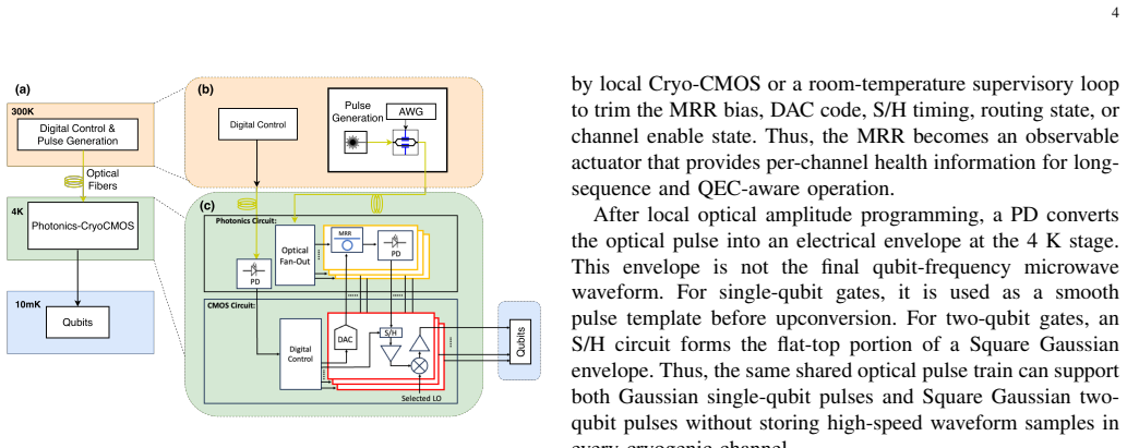
The paper presents a 4 K hybrid photonic/CMOS controller architecture in which optical fibers distribute shared shaped pulse templates while local Cryo-CMOS circuits provide transmission control, amplitude programming, sample-and-hold envelope shaping, LO-tone and phase selection, and microwave upconversion. This enables both single-qubit and two-qubit gate generation in the same path. Compared with fully Cryo-CMOS controllers, it reduces per-channel active dissipation; compared with purely photonic links, it adds local 4 K programmability for pulse selection, amplitude scaling, timing updates, and LO-phase control while remaining compatible with room-temperature feedback and quantum error c
Load-bearing premise
Local cryogenic CMOS circuits at 4 K can perform transmission control, amplitude programming, sample-and-hold shaping, LO-tone selection, phase control, and upconversion with power dissipation and fidelity impact low enough to preserve the claimed scaling advantage.
Editorial extensions
If this is right
- Per-channel active dissipation falls because high-speed sampled RF/IF waveform synthesis and waveform-memory access move out of each cryogenic channel.
- Local 4 K programmability supports pulse selection, amplitude scaling, timing updates, and LO-phase control within the same control path.
- The architecture remains compatible with room-temperature real-time feedback and quantum error correction workflows.
- Controller-induced fidelity limits stay within acceptable bounds according to three-level transmon simulations.
Reading between the lines
- Systems with thousands of qubits become more practical once the number of optical fibers and cryogenic power lines is minimized through template sharing.
- The same hybrid distribution principle could apply to other quantum platforms that need precise microwave control at millikelvin temperatures.
- Crosstalk between channels sharing an optical template would need direct measurement in a multi-qubit testbed to confirm the scaling projection.
- Integration latency from the optical distribution stage may require adjustments to real-time feedback timing in error-correction loops.
Signed reviews
Editorial analysis
A structured set of objections, weighed in public.
Referee Report
Summary. The manuscript proposes a 4 K hybrid photonic/CMOS controller architecture for superconducting qubits in which optical fibers distribute shared shaped pulse templates while local Cryo-CMOS circuits perform transmission gating, amplitude programming, sample-and-hold envelope shaping, LO-tone/phase selection, and microwave upconversion. Architecture-level first-order analytic models for power dissipation, waveform-memory scaling, and controller-induced infidelity are presented together with a three-level transmon simulation of dominant error terms; the analysis concludes that the hybrid approach is a feasible path to scalable control that reduces per-channel dissipation relative to all-Cryo-CMOS designs while retaining local programmability absent from purely photonic links.
Significance. If the first-order models prove accurate, the architecture would offer a concrete route to lowering cryogenic wiring count and active power per channel while preserving real-time feedback compatibility, addressing a central scaling bottleneck for superconducting processors.
major comments (3)
- [Abstract] Abstract and the analysis section: the feasibility conclusion rests on 'architecture-level first-order models' for 4 K power dissipation and fidelity limits, yet no explicit equations, numerical outputs, error budgets, or sensitivity analyses on key parameters (mixer conversion loss, hold-capacitor leakage, LO distribution power, upconversion efficiency at 4 K) are supplied, so the claimed per-channel power reduction and scaling advantage cannot be evaluated.
- [Abstract] The three-level transmon simulation is invoked to cross-check dominant fidelity terms, but the manuscript provides neither the simulation parameters, the extracted infidelity values, nor a comparison against the analytic model predictions, leaving the fidelity claim unsupported.
- The central scaling advantage requires that local 4 K CMOS simultaneously implement all listed functions (transmission control through microwave upconversion) with total dissipation and added infidelity low enough to outperform both baselines; the paper supplies only first-order estimates without SPICE-level netlists, published 4 K Cryo-CMOS measurements for the upconversion/phase blocks, or any validation that the implicit assumptions hold within the required margins.
minor comments (1)
- Notation for the optical pulse templates and the local envelope programming blocks should be defined consistently before the first-order models are introduced.
Simulated Author's Rebuttal
We thank the referee for the constructive feedback on our manuscript. We address each major comment below and agree that expanding the presentation of the models and simulation results will strengthen the paper.
read point-by-point responses
-
Referee: [Abstract] Abstract and the analysis section: the feasibility conclusion rests on 'architecture-level first-order models' for 4 K power dissipation and fidelity limits, yet no explicit equations, numerical outputs, error budgets, or sensitivity analyses on key parameters (mixer conversion loss, hold-capacitor leakage, LO distribution power, upconversion efficiency at 4 K) are supplied, so the claimed per-channel power reduction and scaling advantage cannot be evaluated.
Authors: The manuscript presents architecture-level first-order analytic models in the analysis section, but we agree these are summarized at too high a level in the abstract and lack explicit equations and numerical detail. In revision we will add the governing equations for power dissipation and infidelity, sample numerical outputs for representative parameters, an error budget table, and sensitivity analysis on the listed parameters (mixer loss, leakage, LO power, upconversion efficiency). revision: yes
-
Referee: [Abstract] The three-level transmon simulation is invoked to cross-check dominant fidelity terms, but the manuscript provides neither the simulation parameters, the extracted infidelity values, nor a comparison against the analytic model predictions, leaving the fidelity claim unsupported.
Authors: We will include the transmon simulation parameters (levels, drive strengths, decoherence rates), the extracted infidelity values for each error term, and a direct side-by-side comparison with the analytic model predictions in the revised manuscript. revision: yes
-
Referee: [—] The central scaling advantage requires that local 4 K CMOS simultaneously implement all listed functions with total dissipation and added infidelity low enough to outperform both baselines; the paper supplies only first-order estimates without SPICE-level netlists, published 4 K Cryo-CMOS measurements for the upconversion/phase blocks, or any validation that the implicit assumptions hold within the required margins.
Authors: The work is explicitly scoped as an architecture-level proposal using first-order estimates; circuit-level SPICE netlists and new 4 K measurements lie outside this scope. We will add an expanded discussion of the key assumptions, their validity ranges, and the conditions under which the scaling advantage holds, while clearly stating that detailed circuit validation remains future work. revision: partial
Circularity Check
No circularity detected; claims rest on external architectural comparisons
full rationale
The manuscript advances an architectural proposal supported by first-order analytic models for power, memory scaling, and fidelity, plus a three-level transmon simulation for error cross-checks. No derivation steps, equations, or fitted parameters are presented that reduce any claimed prediction or feasibility result to the inputs by construction. No self-citation chains, uniqueness theorems, or ansatzes imported from prior author work appear as load-bearing elements. The central feasibility argument compares the hybrid approach against fully Cryo-CMOS and purely photonic baselines using independent modeling assumptions, rendering the derivation self-contained.
Assumptions & free parameters
Cite this review
Pith. "Pith review of A Cryogenic Hybrid Photonic/CMOS Controller Architecture for Scalable Superconducting Qubit Control." pith.science (2026). https://pith.science/paper/23BP7ZNQ
@misc{pith2026260610114,
  author       = {Pith},
  title        = {Pith review of: A Cryogenic Hybrid Photonic/CMOS Controller Architecture for Scalable Superconducting Qubit Control},
  year         = {2026},
  howpublished = {\url{https://pith.science/paper/23BP7ZNQ}},
  note         = {Machine review of arXiv:2606.10114}
}
read the original abstract
Scaling superconducting quantum computers toward thousands of qubits remains a difficult control hardware problem. It requires hardware that reduces room-temperature to cryogenic wiring and cryogenic power while preserving in-fridge programmability for microwave pulse generation. This work develops a 4 K hybrid photonic/CMOS control architecture in which optical fibers distribute shared shaped pulse templates, while local cryogenic CMOS (Cryo-CMOS) circuits provide transmission control, amplitude programming, sample-and-hold envelope shaping, LO-tone and phase selection, and microwave upconversion, enabling both single-qubit and two-qubit gate generation within the same control path. Compared with fully Cryo-CMOS controllers, this architecture reduces per-channel active dissipation by moving high-speed sampled RF/IF waveform synthesis and waveform-memory access out of each cryogenic channel. Compared with purely photonic-link qubit-control approaches, it adds local 4 K programmability for pulse selection, amplitude scaling, timing updates, and LO-phase control, while remaining compatible with room-temperature real-time feedback and quantum error correction (QEC) workflows. We present architecture-level first-order models for 4 K power dissipation, waveform-memory scaling, and controller-induced fidelity limits, and cross-check the dominant fidelity terms using a three-level transmon simulation. The analysis shows that shared optical pulse template distribution with local 4 K envelope programming is a feasible path toward scalable superconducting qubit control.
Figures


Figures from the paper (5 more)


Forward citations
Cited by 1 Pith paper
-
Onnes: A Physics-Grounded Multi-Agent LLM Simulator for Cryogenic Fault Diagnosis in Quantum Computing Infrastructure
A physics-grounded dilution-fridge simulator with LLM agents achieves supervised-ML parity on cryogenic fault classification using six demonstrations and no training, validated on simulated telemetry plus a real-hardw...
Reference graph
Works this paper leans on
-
[1]
Establishing a new benchmark in quantum computational advantage with 105-qubit zuchongzhi 3.0 processor,
D. Gao, D. Fan, C. Zha, J. Bei, G. Cai, J. Cai, S. Cao, X. Zeng, F. Chen, J. Chenet al., “Establishing a new benchmark in quantum computational advantage with 105-qubit zuchongzhi 3.0 processor,”Physical Review Letters, vol. 134, p. 090601, 2025
2025
-
[2]
Engineering cryogenic setups for 100-qubit scale superconducting circuit systems,
S. Krinner, S. Storz, P. Kurpiers, P. Magnard, J. Heinsoo, R. Keller, J. L ¨utolf, C. Eichler, and A. Wallraff, “Engineering cryogenic setups for 100-qubit scale superconducting circuit systems,”EPJ Quantum Technology, vol. 6, no. 2, 2019
2019
-
[3]
Scaling up superconducting quantum com- puters with cryogenic rf-photonics,
S. Joshi and S. Moazeni, “Scaling up superconducting quantum com- puters with cryogenic rf-photonics,”Journal of Lightwave Technology, vol. 42, no. 1, pp. 166–175, 2024
2024
-
[4]
Design and characterization of a 28-nm bulk-cmos cryogenic quantum controller dissipating less than 2 mw at 3 k,
J. C. Bardin, E. Jeffrey, E. Lucero, T. Huang, S. Das, D. Sank, O. Naaman, A. Megrant, R. Barends, T. Whiteet al., “Design and characterization of a 28-nm bulk-cmos cryogenic quantum controller dissipating less than 2 mw at 3 k,”IEEE Journal of Solid-State Circuits, vol. 54, no. 11, pp. 3043–3060, 2019
2019
-
[5]
A cryo-cmos low-power semi-autonomous transmon qubit state controller in 14-nm finfet technology,
S. Chakraborty, D. J. Frank, K. Tien, P. Rosno, M. Yeck, J. A. Glick, R. Robertazzi, R. Richetta, J. F. Bulzacchelli, D. Underwoodet al., “A cryo-cmos low-power semi-autonomous transmon qubit state controller in 14-nm finfet technology,”IEEE Journal of Solid-State Circuits, vol. 57, no. 11, pp. 3258–3273, 2022
2022
-
[6]
A scalable cryo-cmos controller for the wideband frequency- multiplexed control of spin qubits and transmons,
J. P. G. van Dijk, B. Patra, S. Subramanian, X. Xue, N. Samkharadze, A. Corna, C. Jeon, F. Sheikh, E. Juarez-Hernandez, B. P. Esparza et al., “A scalable cryo-cmos controller for the wideband frequency- multiplexed control of spin qubits and transmons,”IEEE Journal of Solid-State Circuits, vol. 55, no. 11, pp. 2930–2946, 2020
2020
-
[7]
Control and readout of a superconducting qubit using a photonic link,
F. Lecocq, F. Quinlan, K. Cicak, J. Aumentado, S. A. Diddams, and J. D. Teufel, “Control and readout of a superconducting qubit using a photonic link,”Nature, vol. 591, no. 7851, pp. 575–579, 2021
2021
-
[8]
Microwaves in quantum computing,
J. C. Bardin, D. H. Slichter, and D. J. Reilly, “Microwaves in quantum computing,”IEEE Journal of Microwaves, vol. 1, no. 1, pp. 403–427, 2021
2021
Show all 52 references
-
[9]
Feedback control of a solid-state qubit using high-fidelity projective measurement,
D. Rist `e, C. C. Bultink, K. W. Lehnert, and L. DiCarlo, “Feedback control of a solid-state qubit using high-fidelity projective measurement,” Physical Review Letters, vol. 109, p. 240502, 2012
2012
-
[10]
Low-latency digital signal processing for feedback and feedforward in quantum computing and communication,
Y . Salath ´e, P. Kurpiers, T. Karg, C. K. Lang, P. Magnard, J. Heinsoo, S. Storz, J.-C. Besse, A. Mezzacapo, U. Las Heraset al., “Low-latency digital signal processing for feedback and feedforward in quantum computing and communication,”Physical Review Applied, vol. 9, p. 034...
2018
-
[11]
Surface codes: Towards practical large-scale quantum computation,
A. G. Fowler, M. Mariantoni, J. M. Martinis, and A. N. Cleland, “Surface codes: Towards practical large-scale quantum computation,”Physical Review A, vol. 86, no. 3, p. 032324, 2012
2012
-
[12]
Demonstrating real-time and low-latency quan- tum error correction with superconducting qubits,
L. Cauneet al., “Demonstrating real-time and low-latency quan- tum error correction with superconducting qubits,”arXiv preprint arXiv:2410.05202, 2024
2024
-
[13]
Fault-tolerant quantum comput- ing in the pauli or clifford frame with slow error diagnostics,
C. Chamberland, P. Iyer, and D. Poulin, “Fault-tolerant quantum comput- ing in the pauli or clifford frame with slow error diagnostics,”Quantum, vol. 2, p. 43, 2018
2018
-
[14]
Quantum error correction below the surface code threshold,
R. e. a. Acharya, “Quantum error correction below the surface code threshold,”Nature, vol. 638, pp. 920–926, 2025
2025
-
[15]
Cryogenic optical-to-microwave conversion using si photonic integrated circuit ge photodiodes,
D. Julien-Neitzert, E. Leung, N. Islam, S. Khorev, S. Shekhar, L. Chros- towski, J. F. Young, and J. Salfi, “Cryogenic optical-to-microwave conversion using si photonic integrated circuit ge photodiodes,”APL Photonics, vol. 9, no. 11, p. 116107, 2024
2024
-
[16]
Cross-cross resonance gate,
K. Heya, N. Kanazawaet al., “Cross-cross resonance gate,”PRX Quantum, vol. 2, p. 040336, 2021
2021
-
[17]
Procedure for systematically tuning up cross-talk in the cross-resonance gate,
S. Sheldon, E. Magesan, J. M. Chow, and J. M. Gambetta, “Procedure for systematically tuning up cross-talk in the cross-resonance gate,”Physical Review A, vol. 93, p. 060302, 2016
2016
-
[18]
Using cryogenic cmos control electronics to enable a two-qubit cross-resonance gate,
D. L. Underwoodet al., “Using cryogenic cmos control electronics to enable a two-qubit cross-resonance gate,”PRX Quantum, vol. 5, no. 1, p. 010326, 2024
2024
-
[19]
A quantum engineer’s guide to superconducting qubits,
P. Krantz, M. Kjaergaard, F. Yan, T. P. Orlando, S. Gustavsson, and W. D. Oliver, “A quantum engineer’s guide to superconducting qubits,” Applied Physics Reviews, vol. 6, p. 021318, 2019
2019
-
[20]
Systematic improvements in transmon qubit coherence enabled by niobium surface encapsulation,
M. Bal, A. A. Murthy, S. Zhu, F. Crisa, X. You, Z. Huang, T. Roy, J. Lee, D. van Zanten, R. Pilipenkoet al., “Systematic improvements in transmon qubit coherence enabled by niobium surface encapsulation,” npj Quantum Information, vol. 10, p. 43, 2024
2024
-
[21]
Simple pulses for elimination of leakage in weakly nonlinear qubits,
F. Motzoi, J. M. Gambetta, P. Rebentrost, and F. K. Wilhelm, “Simple pulses for elimination of leakage in weakly nonlinear qubits,”Physical Review Letters, vol. 103, p. 110501, 2009
2009
-
[22]
Reducing leakage of single-qubit gates for supercon- ducting quantum processors using analytical control pulse envelopes,
E. Hyypp ¨a, A. Veps ¨al¨ainen, M. Papi ˇc, C. F. Chan, S. Inel, A. Landra, W. Liu, J. Luus, F. Marxer, C. Ockeloen-Korppi, S. Orbell, B. Tarasinski, and J. Heinsoo, “Reducing leakage of single-qubit gates for supercon- ducting quantum processors using analytical control pulse...
2024
-
[23]
Error-robust quantum logic optimization using a cloud quantum computer interface,
A. R. R. Carvalho, H. Ball, M. J. Biercuk, M. R. Hush, and F. Thom- sen, “Error-robust quantum logic optimization using a cloud quantum computer interface,”Physical Review Applied, vol. 15, p. 064054, 2021
2021
-
[24]
Calibration of drive nonlinearity for arbitrary- angle single-qubit gates using error amplification,
S. Laz ˘ar, Q. Ficheux, J. Herrmann, A. Remm, M. Kerschbaum, J.-C. Besse, and A. Wallraff, “Calibration of drive nonlinearity for arbitrary- angle single-qubit gates using error amplification,”Physical Review Applied, vol. 20, p. 024036, 2023
2023
-
[25]
Superconducting quantum circuits at the surface code threshold for fault tolerance,
R. Barends, J. Kelly, A. Megrantet al., “Superconducting quantum circuits at the surface code threshold for fault tolerance,”Nature, vol. 508, pp. 500–503, 2014
2014
-
[26]
Realization of high-fidelity cz gate based on a double- transmon coupler,
R. Liet al., “Realization of high-fidelity cz gate based on a double- transmon coupler,”Physical Review X, vol. 14, p. 041050, 2024
2024
-
[27]
Impact of classical control electronics on qubit fidelity,
J. P. G. van Dijk, A. Vladimirescu, E. Charbon, F. Sebastiano, and H. Homulle, “Impact of classical control electronics on qubit fidelity,” Physical Review Applied, vol. 12, p. 044054, 2019
2019
-
[28]
Microwave-multiplexed qubit controller using adiabatic superconductor logic,
N. Takeuchi, T. Yamae, T. Yamashita, T. Yamamoto, and N. Yoshikawa, “Microwave-multiplexed qubit controller using adiabatic superconductor logic,”npj Quantum Information, vol. 10, p. 59, 2024
2024
-
[29]
Design and fabrication of cryogenic multiplexing control chip,
R. Huang, Y . Shi, X. Geng, L. Yang, J. Liu, and W. Chen, “Design and fabrication of cryogenic multiplexing control chip,”Frontiers in Physics, vol. 11, p. 1212642, 2023
2023
-
[30]
Cryogenic multiplexing control chip for a superconducting quantum processor,
R. Huang, X. Geng, X. Wu, G. Dai, L. Yang, J. Liu, and W. Chen, “Cryogenic multiplexing control chip for a superconducting quantum processor,”Physical Review Applied, vol. 18, p. 064046, 2022
2022
-
[31]
Globalfoundries silicon photonics – gf fotonix 45spclo,
CMC Microsystems, “Globalfoundries silicon photonics – gf fotonix 45spclo,” 2026, technology access page for the GlobalFoundries 45SP- CLO silicon-photonic/CMOS platform
2026
-
[32]
Operation of high-speed silicon photonic micro-disk modulators at cryogenic temperatures,
M. Gehl, C. Long, D. Trotter, A. Starbuck, A. Pomerene, J. B. Wright, S. Melgaard, J. Siirola, A. L. Lentine, and C. DeRose, “Operation of high-speed silicon photonic micro-disk modulators at cryogenic temperatures,”Optica, vol. 4, no. 3, pp. 374–382, 2017
2017
-
[33]
A fully packaged cryogenic optical transmitter directly interfaced with a superconducting chip,
B. Yin, H. Gevorgyan, D. Onural, B. Zhang, A. Khilo, M. A. Popovi ´c, and V . M. Stojanovi´c, “A fully packaged cryogenic optical transmitter directly interfaced with a superconducting chip,”Nature Electronics, vol. 9, pp. 78–83, 2026
2026
-
[34]
Cryo-compatible, silicon spoked- ring modulator in a 45nm cmos platform for 4k-to-room-temperature optical links,
H. Gevorgyan, A. Khilo, D. Van Orden, D. Onural, B. Yin, M. T. Wade, V . M. Stojanovic, and M. A. Popovic, “Cryo-compatible, silicon spoked- ring modulator in a 45nm cmos platform for 4k-to-room-temperature optical links,” inOptical Fiber Communication Conference, 2021, p. M3B.3
2021
-
[35]
Sub-decibel efficiency, bi-layer, o-band fiber-to-chip grating coupler demonstrated in a 45 nm cmos foundry platform,
B. Zhanget al., “Sub-decibel efficiency, bi-layer, o-band fiber-to-chip grating coupler demonstrated in a 45 nm cmos foundry platform,” in CLEO: Science and Innovations, 2022, demonstrated 0.85 dB O-band fiber-to-chip grating coupler in a 45 nm CMOS foundry platform. 14
2022
-
[36]
Cryogenic optical packaging using photonic wire bonds,
B. Lin, D. Witt, J. F. Young, and L. Chrostowski, “Cryogenic optical packaging using photonic wire bonds,”APL Photonics, vol. 8, p. 126109, 2023
2023
-
[37]
Scalable low loss cryogenic packaging of quantum memories in cmos-foundry processed photonic chips,
R. Bernson, A. Witte, G. Clark, K. Gradkowski, J. Yang, M. Saha, M. Zimmermann, A. Leenheer, K. C. Chen, G. Gilbert, M. Eichenfield, D. Englund, and P. O’Brien, “Scalable low loss cryogenic packaging of quantum memories in cmos-foundry processed photonic chips,”arXiv preprint ...
2025
-
[38]
A cryogenic cmos chip for generating control signals for multiple qubits,
S. J. Pauka, K. Das, R. Kalra, A. Moini, Y . Yang, M. Trainer, A. Bous- quet, C. Cantaloube, N. Dick, G. C. Gardneret al., “A cryogenic cmos chip for generating control signals for multiple qubits,”Nature Electronics, vol. 4, pp. 64–70, 2021
2021
-
[39]
Bidirectional interconversion of microwave and light with thin-film lithium niobate,
Y . Xu, A. A. Sayem, L. Fan, C.-L. Zou, S. Wang, R. Cheng, W. Fu, L. Yang, M. Xu, and H. X. Tang, “Bidirectional interconversion of microwave and light with thin-film lithium niobate,”Nature Commu- nications, vol. 12, p. 4453, 2021
2021
-
[40]
Cavity electro- optics in thin-film lithium niobate for efficient microwave-to-optical transduction,
J. Holzgrafe, N. Sinclair, D. Zhu, A. Shams-Ansari, M. Colangelo, Y . Hu, M. Zhang, K. K. Berggren, and M. Lon ˇcar, “Cavity electro- optics in thin-film lithium niobate for efficient microwave-to-optical transduction,”Optica, vol. 7, no. 12, pp. 1714–1720, 2020
2020
-
[41]
Coherent control of a superconducting qubit using light,
H. K. Warner, J. Holzgrafe, B. Yankelevich, D. Barton, S. Poletto, C. J. Xin, N. Sinclair, D. Zhu, E. Sete, B. Langley, E. Batson, M. Colangelo, A. Shams-Ansari, G. Joe, K. K. Berggren, L. Jiang, M. Reagor, and M. Lon ˇcar, “Coherent control of a superconducting qubit using li...
2025
-
[42]
All-optical superconducting qubit readout,
G. M. Arnold, T. Werner, R. Sahu, L. N. Kapoor, L. Qiu, and J. M. Fink, “All-optical superconducting qubit readout,”Nature Physics, vol. 21, pp. 393–400, 2025
2025
-
[43]
Optical readout of a superconducting qubit using a piezo-optomechanical transducer,
T. C. van Thiel, M. J. Weaver, F. Berto, P. Duivestein, M. Lemang, K. L. Schuurman, M. Zemlicka, F. Hijazi, A. C. Bernasconi, C. Ferrer, E. Lachman, M. Field, Y . Mohan, F. K. de Vries, C. C. Bultink, J. van Oven, J. Y . Mutus, R. Stockill, and S. Groeblacher, “Optical readout...
2025
-
[44]
An interior-ridge silicon microring modulator,
E. Timurdogan, C. M. Sorace-Agaskar, E. S. Hosseini, and M. R. Watts, “An interior-ridge silicon microring modulator,”Journal of Lightwave Technology, vol. 31, no. 24, pp. 3907–3914, 2013
2013
-
[45]
Resolving the thermal challenges for silicon microring resonator devices,
K. Padmaraju and K. Bergman, “Resolving the thermal challenges for silicon microring resonator devices,”Nanophotonics, vol. 3, no. 4–5, pp. 269–281, 2014
2014
-
[46]
Thermal stabilization of a microring modulator using feedback control,
K. Padmaraju, J. Chan, D. F. Logan, A. P. Knights, and K. Bergman, “Thermal stabilization of a microring modulator using feedback control,” Optics Express, vol. 20, no. 27, pp. 27 999–28 008, 2012
2012
-
[47]
Wavelength locking of silicon photonics multiplexer for dml-based wdm transmitter,
S. Grillanda, F. Morichetti, M. Carminati, P. Ciccarella, M. J. Strain, M. Sorel, and A. Melloni, “Wavelength locking of silicon photonics multiplexer for dml-based wdm transmitter,” in2017 IEEE Photonics Conference (IPC), 2017, pp. 541–542
2017
-
[48]
A 20-ghz low-noise rf pulse generator for silicon quantum computer with 137.4-fs jitter,
T. Norimatsu, Y . Wachi, T. Miki, Y . Kanno, R. Takahashi, T. Ogawa, T. Utsugi, T. Sekiguchi, M. Nagata, and H. Mizuno, “A 20-ghz low-noise rf pulse generator for silicon quantum computer with 137.4-fs jitter,” IEICE Transactions on Electronics, 2025, advance online publication
2025
-
[49]
Multiplexed superconducting qubit control at millikelvin temperatures with a low-power cryo-cmos multiplexer,
R. Acharya, S. Brebels, A. Grill, J. Verjauw, T. Ivanov, D. P. Lozano, D. Wan, J. V . Damme, A. M. Vadiraj, M. Mongillo, B. Govoreanu, J. Craninckx, I. P. Radu, K. de Greve, G. Gielen, F. Catthoor, and A. Poto ˇcnik, “Multiplexed superconducting qubit control at millikelvin te...
2023
-
[50]
QuTiP 5: The quantum toolbox in Python,
N. Lambert, E. Gigu `ere, P. Menczel, B. Li, P. Hopf, G. Su ´arez, M. Gali, J. Lishman, R. Gadhvi, R. Agarwal, A. Galicia, N. Shammah, P. D. Nation, J. R. Johansson, S. Ahmed, S. Cross, A. Pitchford, and F. Nori, “QuTiP 5: The quantum toolbox in Python,”Physics Reports, vol. 1...
2026
-
[51]
Non-volatile tuning of cryogenic silicon photonic micro-ring modulators,
U. Adya, S. Singhal, R. Chen, I.-T. Chen, S. Joshi, A. Majumdar, M. Li, and S. Moazeni, “Non-volatile tuning of cryogenic silicon photonic micro-ring modulators,”Nature Communications, vol. 16, p. 9290, 2025
2025
-
[52]
Fiber array to chip attach using laser fusion splicing for low loss,
J. Nauriyal, M. Song, Y . Zhang, M. Granados-Baez, and J. Cardenas, “Fiber array to chip attach using laser fusion splicing for low loss,” Optics Express, vol. 31, no. 13, pp. 21 863–21 869, 2023
2023
Reviewed June 27, 2026 · model on record in the stance chip above.
Discussion (0). Continue with ORCID to comment.