REVIEW 4 major objections 4 minor 1 cited by
Development of an MKID frequency-to-pixel LED mapper for SPT-3G+
T0 review · 4 major / 4 minor · reviewed 2026-08-12 · deepseek-v4-flash
Pith's one-line read A cryogenic 30-LED mapper identifies which microwave resonance belongs to which physical pixel on SPT-3G+ prototype MKID arrays at 320 mK, exposing fabrication scatter that limits detector yield.
desk verdict Solid, incremental instrumentation work: the LED mapper works at 320 mK and handles multiple pixels per LED, but the paper never validates assignment accuracy, so its fabrication-defect interpretation is weaker than the basic mapping claim. read the letter →
The pith
A machine-rendered reading of the paper's core claim, the machinery that carries it, and where it could break.
The reading
What carries the argument
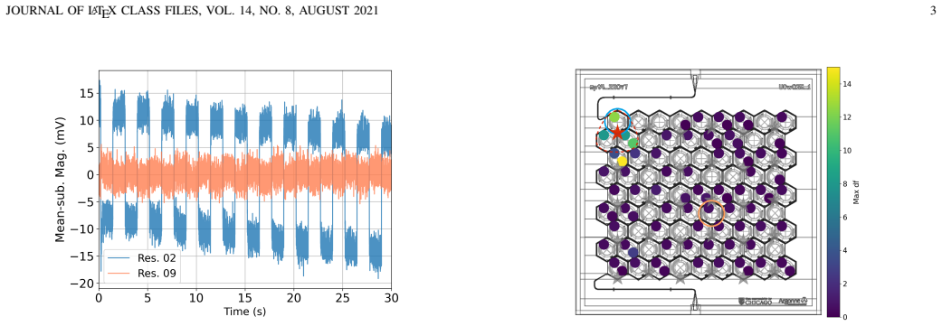
The central object is the LED mapper itself: a printed circuit board with 30 LEDs addressed through a row-column scheme, a plastic spacer, and an aluminum collimating lid with 1.6 mm holes that guides each LED's light to a hexagonal unit cell of three pixels while blocking stray light. Because the 2.2 mm pixel pitch prevents one LED per pixel, the design exploits the existing frequency-bank structure: each unit cell contains six detectors (two polarizations per pixel) spread across six deliberately separated frequency banks, so one LED can identify up to one resonator per bank. The mapping procedure works by placing bias tones on each resonance, flashing one LED at 0.4 Hz with 50% duty cycle for 30 seconds, converting I/Q timestreams into frequency-shift PSDs, and assigning to each LED the resonance in each bank whose response exceeds the mean by 10 sigma, with a crosscheck that only one resonance per bank is assigned per LED.
What would settle it
Mask off one LED's collimator hole so no light reaches the wafer, flash it at the usual rate, and look for any resonator whose response exceeds the 10-sigma threshold; a positive result would prove that non-optical crosstalk alone can create a match, invalidating the strongest-response assignment rule.
Extended reading notes
Core claim
The central claim is that a simple fixture of 30 blue LEDs, a row-column addressing board, and a collimating lid can produce a reliable frequency-to-pixel map for SPT-3G+ prototype MKID arrays even at 320 mK, well above the 100 mK design temperature. On a prototype 220 GHz chip of 160 MKIDs, the authors show that flashing each LED in turn and measuring the frequency shift of every resonance yields a map in which the strongest responding resonator in each frequency bank sits in the illuminated unit cell, with matches accepted only above a 10-sigma threshold and one assignment per bank per LED. The maps reproduce the intended six-bank ordering and expose three classes of fabrication defects: resonators that clash at nearly the same frequency, resonators that are missing entirely, and resonators that have swapped positions relative to the design. They also reveal that measured frequencies curve downward across each bank with position, indicating a spatial fabrication non-uniformity, and that '×'-oriented inductors sit about 10 MHz higher than '+' ones, an effect absent from the first bank because of a mask error shorting one orientation. Together these results establish the mapper as both a yield diagnostic and the foundation for a subsequent capacitor-trimming step.
Load-bearing premise
The whole map rests on assuming that the resonator with the strongest response to an LED flash is the pixel under that LED; if stray light or electrical crosstalk ever produces the largest response, the assignment is wrong.
Editorial extensions
If this is right
- Guided by the frequency-to-pixel map, interdigitated-capacitor trimming can move clashed and swapped resonators onto the intended 566 kHz grid, raising the sub-module yield from 81% toward the >90% goal.
- Because the mapping succeeds at 320 mK, prototype arrays can be tested in a helium sorption cryostat, freeing the dilution refrigerator for low-noise measurements.
- The maps serve as a spatial fabrication diagnostic, showing where frequency drift is correlated with position and where the '×' inductor orientation sits systematically higher in frequency than the '+' orientation.
- A mapper built at the scale of a full SPT-3G+ triangular sub-module would apply the same mapping-and-trimming process to the deployment-scale arrays with 800 detectors per readout channel.
Reading between the lines
- One extension the authors leave implicit is using each LED's spatial point-spread to predict a response profile across neighboring pixels, which would quantify stray-light contamination per LED instead of relying on a single 10-sigma cutoff.
- The downward frequency drift across each bank is smooth in position, which suggests a wafer-level correction map could be applied before trimming and reduce the number of required trimming iterations.
- The reproducible ~10 MHz offset between the two inductor orientations could be tracked as a manufacturing-quality metric across wafers, independent of any particular science run.
- A natural testable variant would flash multiple LEDs with orthogonal codes and deconvolve the responses, turning 30 sequential 30-second exposures into a single multiplexed mapping pass.
Editorial analysis
A structured set of objections, weighed in public.
Referee Report
Summary. This manuscript describes a cryogenic LED-based frequency-to-pixel mapper for prototype SPT-3G+ MKID arrays. A printed circuit board with 30 LEDs, a spacer, and a collimating lid illuminates unit cells on a 1-inch chip at 320 mK, while the RF-ICE readout records I/Q timestreams during 0.4 Hz LED flashing. Resonances are identified from sparse and fine sweeps, bias tones are placed, and the frequency-to-pixel map is constructed by assigning, for each LED, the strongest responding resonance in each frequency bank above a 10σ threshold. The authors show a chopped optical response, a monotonic response versus LED power, and a spatial map of assigned pixel locations. They then use the map to diagnose resonator frequency scatter, including missing, clashed, and swapped resonators, and propose a two-step process of mapping and IDC trimming to improve detector yield. The central claim is that this mapper works at 300-320 mK and provides a usable frequency-to-pixel map for SPT-3G+ prototype arrays.
Significance. If the mapping is accurate, the result is genuinely useful for SPT-3G+ development: a direct identification of which resonance belongs to which physical pixel, obtained at a relatively high operating temperature, enables both resonator-scatter diagnostics and post-fabrication frequency trimming. The work builds naturally on the LED-mapping concept of Liu et al. and the cryogenic LED module of Shroyer et al., and it extends those ideas to the SPT-3G+ pixel geometry with six detectors per unit cell in six frequency banks. The manuscript gives clear visual evidence that flashed LEDs produce a strong, localized response and that the resulting maps reveal real structure in the resonator frequency scatter. The main weakness is that the assignment accuracy is never quantitatively established: no confusion matrix, repeatability statistic, or comparison to an independent known-good map is provided, even though the assignment rule is the load-bearing element for the proposed trimming application. The paper also includes useful machine-readable-style diagnostics in the figures, but no code or data release is mentioned.
major comments (4)
- [Section II-C and Fig. 7] The assignment rule in Section II-C (accept only the strongest resonance per bank above 10σ, one resonance per bank per LED) has no accompanying accuracy metric. Figure 7 itself shows the failure mode: a resonance outside the active LED's unit cell has a strong response, attributed to stray light on a very responsive detector. If that resonance were the largest in its frequency bank, the rule would assign it to the wrong LED. Because Figure 8 then labels missing, clashed, and swapped resonators using this same map, an assignment error is indistinguishable from a fabrication defect. Please provide an external validation: for example, repeat the mapping multiple times and report the fraction of assignments that change between runs, or compare the map against a known-good map obtained by a different method, or report a confusion matrix with a measured false-assignment rate as a function of the 10σ threshold.
- [Section II-C and Fig. 5] The crosschecks mentioned in Section II-C are not described, and the level of crosstalk is only illustrated qualitatively in Figure 5. Since the assignment rule relies on the strongest response being the true optical signal, the paper should quantify how often the 10σ threshold changes the assignment relative to a pure per-bank maximum, and should bound the contribution of electrical crosstalk and stray light to the measured timestream amplitudes. Without such a test, it is not possible to assess whether the mapping procedure is reliable enough for the IDC-trimming yield goals stated in Section VI-B.
- [Section IV and Fig. 8] The frequency-scatter analysis in Figure 8 reports no measurement uncertainties for the resonator frequencies, and the criteria for classifying a resonator as missing, clashed, or swapped are not stated. Please report the frequency measurement uncertainty (from the fine sweep and tone placement), the tolerance used to define a clash, and the number of resonators in each category. This is needed to distinguish real fabrication scatter from mapper artifacts.
- [Section VI-B] The yield statement in Section VI-B ('so far attained a yield of 81% after removing one half of all collisions. If all resonances in collisions could be preserved and reordered, the yield would increase to > 90%') is presented without a reference or a description of how the yield was measured. Please either cite the supporting measurement or label this as an estimate from unpublished prototype data, and specify the number of arrays and detectors used.
minor comments (4)
- [Abstract and Section II-B] The abstract states that mapping is demonstrated at 300 mK, while Section II-B reports a base temperature of 320 mK and the conclusion repeats 320 mK. Please make these numbers consistent.
- [Section I] Two references are missing in the sentence about the cause of resonance scatter ('generally believed to stem from inconsistencies during the fabrication process, but the exact mechanism is often difficult to pinpoint [?], [?]'). Please fill in these references or remove the placeholder.
- [Section II-C] The sentence 'Crosschecks are implemented to prevent mis-assignment due to variations in detector responsitivity' is vague. Please specify what the crosschecks actually compare and how often they change a raw maximum-response assignment.
- [Fig. 6] The power-dependence figure would be more informative with a single resonance's frequency shift plotted against LED drive voltage or current, rather than only a family of curves with a legend; this would make it easier to see whether the response is monotonic and where it begins to saturate.
Circularity Check
No significant circularity: the frequency-to-pixel map is a direct measurement, not a derived prediction.
full rationale
The paper's central claim is an experimental demonstration: an LED illuminates a unit cell, and the MKID with the strongest response in each frequency bank is assigned to that physical location. This assignment is the operational definition of the frequency-to-pixel map, not a prediction derived from a fitted parameter. No model parameter is fit to a subset of the data and then used to predict a closely related quantity; the 10-sigma acceptance threshold is a data-quality cut, and the only external comparison in Section IV is against the design mask and Sonnet simulation, which are independent of the measured map. The stray-light event in Fig. 7 is an acknowledged validation limitation, but a wrong assignment from stray light would be an experimental error, not a tautology. Self-citations [1]-[4] and [7] support the SPT-3G+ detector design and RF-ICE readout hardware, while the LED-mapping technique itself is grounded in independent prior work [5] and [8]. Thus the derivation chain is self-contained for what it claims: a measured frequency-to-pixel map and a diagnostic look at resonator scatter.
Assumptions & free parameters
free parameters (1)
- match acceptance threshold =
10 sigma
assumptions (3)
- domain assumption Each LED illuminates only its intended unit cell, and stray light is weak enough that the highest-response resonance identifies the correct pixel.
- domain assumption The MKID frequency response during LED flashing is dominated by optical absorption in the intended pixel, not by thermal or electrical crosstalk.
- domain assumption Sonnet-simulated designed resonance frequencies are accurate enough that deviations from the intended order indicate real fabrication scatter (missing, clashed, swapped resonators).
Cite this review
Pith. "Pith review of Development of an MKID frequency-to-pixel LED mapper for SPT-3G+." pith.science (2026). https://pith.science/paper/PVVTYT2J
@misc{pith2026241117878,
  author       = {Pith},
  title        = {Pith review of: Development of an MKID frequency-to-pixel LED mapper for SPT-3G+},
  year         = {2026},
  howpublished = {\url{https://pith.science/paper/PVVTYT2J}},
  note         = {Machine review of arXiv:2411.17878}
}
read the original abstract
SPT-3G+ is the next-generation camera for the South Pole Telescope (SPT). SPT is designed to measure the cosmic microwave background (CMB) and the mm/sub-mm sky. The planned focal plane consists of 34,000 microwave kinetic inductance detectors (MKIDs), divided among three observing bands centered at 220, 285, and 345 GHz. Each readout line is designed to measure 800 MKIDs over a 500 MHz bandwidth, which places stringent constraints on the accuracy of the frequency placement required to limit resonator collisions that reduce the overall detector yield. To meet this constraint, we are developing a two-step process that first optically maps the resonance to a physical pixel location, and then next trims the interdigitated capacitor (IDC) to adjust the resonator frequency. We present a cryogenic LED apparatus operable at 300 mK for the optical illumination of SPT-3G+ detector arrays. We demonstrate integration of the LED controls with the GHz readout electronics (RF-ICE) to take data on an array of prototype SPT-3G+ detectors. We show that this technique is useful for characterizing defects in the resonator frequency across the detector array and will allow for improvements in the detector yield.
Figures


Figures from the paper (3 more)


Forward citations
Cited by 1 Pith paper
-
Automated analysis of the visual properties of superconducting detectors
A computer-vision pipeline for room-temperature optical screening of MKID detector wafers reports 98.6% simulated defect-detection accuracy, yet its predicted yields on two real chips were far from cryogenic measurements.
Reference graph
Works this paper leans on
-
[1]
SPT-3G+: mapping the high-frequency cosmic microwave background using kinetic inductance detectors,
A. J. Anderson, P. Barry, A. N. Bender, B. A. Benson, L. E. Bleem, J. E. Carlstrom, T. W. Cecil, C. L. Chang, T. M. Crawford, K. R. Dibert, M. A. Dobbs, K. Fichman, N. W. Halverson, W. L. Holzapfel, A. Hryciuk, K. S. Karkare, J. Li, M. Lisovenko, D. Marrone, J. McMahon, J. Montgomery, T. Natoli, Z. Pan, S. Raghunathan, C. L. Reichardt, M. Rouble, E. Shiro...
work page 2022
-
[2]
B. A. Benson, P. a. R. Ade, Z. Ahmed, S. W. Allen, K. Arnold, J. E. Austermann, A. N. Bender, L. E. Bleem, J. E. Carlstrom, C. L. Chang, H. M. Cho, J. F. Cliche, T. M. Crawford, A. Cukierman, T. d. Haan, M. A. Dobbs, D. Dutcher, W. Everett, A. Gilbert, N. W. Halverson, D. Hanson, N. L. Harrington, K. Hattori, J. W. Henning, G. C. Hilton, G. P. Holder, W. ...
work page 2014
-
[3]
Characterization of MKIDs for CMB observation at 220 GHz with the South Pole Telescope
K. R. Dibert, P. S. Barry, A. J. Anderson, B. A. Benson, T. Cecil, C. L. Chang, K. N. Fichman, K. Karkare, J. Li, T. Natoli, Z. Pan, M. Rouble, E. Shirokoff, and M. Young, “Characterization of MKIDs for CMB observation at 220 GHz with the South Pole Telescope,” IEEE Transactions on Applied Superconductivity , vol. 33, no. 5, pp. 1–5, Aug. 2023, arXiv:2304...
work page Pith review arXiv 2023
-
[4]
K. Dibert, P. Barry, Z. Pan, A. Anderson, B. Benson, C. Chang, K. Karkare, J. Li, T. Natoli, M. Rouble, E. Shirokoff, and A. Stark, “Development of MKIDs for measurement of the Cosmic Microwave Background with the South Pole Telescope,” Journal of Low Temperature Physics, vol. 209, no. 3-4, pp. 363–371, Nov. 2022, arXiv:2111.04816 [astro-ph]. [Online]. Av...
work page Pith review arXiv 2022
-
[5]
Cryogenic LED pixel-to-frequency mapper for kinetic inductance detector arrays,
X. Liu, W. Guo, Y . Wang, L. F. Wei, C. M. Mckenney, B. Dober, T. Billings, J. Hubmayr, L. S. Ferreira, M. R. Vissers, and J. Gao, “Cryogenic LED pixel-to-frequency mapper for kinetic inductance detector arrays,” Journal of Applied Physics , vol. 122, no. 3, p. 034502, Jul. 2017, publisher: American Institute of Physics. [Online]. Available: https://aip.s...
-
[6]
——, “Supplementary Materials for “Cryogenic LED pixel-to-frequency mapper for kinetic inductance detector arrays”,” p. 2
-
[7]
M. Rouble, G. Smecher, A. Anderson, P. S. Barry, K. Dibert, M. Dobbs, K. S. Karkare, and J. Montgomery, “RF-ICE: large-scale gigahertz readout of frequency-multiplexed microwave kinetic inductance detectors,” in Millimeter, Submillimeter, and Far-Infrared Detectors and Instrumentation for Astronomy XI , vol. 12190. SPIE, Aug. 2022, pp. 898–911. [Online]. ...
work page 2022
-
[8]
A scalable cryogenic LED module for selectively illuminating kinetic inductance detector arrays,
J. E. Shroyer, M. Nelson, L. Walters, and B. R. Johnson, “A scalable cryogenic LED module for selectively illuminating kinetic inductance detector arrays,” Review of Scientific Instruments , vol. 93, no. 11, p. 113107, Nov. 2022. [Online]. Available: https://doi.org/10.1063/5. 0103968
doi:10.1063/5 2022
Reviewed August 12, 2026 · model on record in the stance chip above.
Discussion (0). Continue with ORCID to comment.