REVIEW 3 major objections 4 minor 82 references
Growth of hexagonal BN crystals by traveling-solvent floating zone
T0 review · 3 major / 4 minor · reviewed 2026-08-11 · deepseek-v4-flash
Pith's one-line read Traveling-solvent floating zone grows high-quality hexagonal BN crystals.
desk verdict Solid first demonstration of TSFZ growth of h-BN; feasibility holds, but the 'on par with CBF' claim outruns the stacking-fault evidence. read the letter →
The pith
A machine-rendered reading of the paper's core claim, the machinery that carries it, and where it could break.
The reading
What carries the argument
The central object is the traveling-solvent floating zone (TSFZ) itself: a molten iron flux is held between a feed rod and a seed rod without a crucible; the feed rod dissolves into the flux, and h-BN recrystallizes onto the seed as the molten zone is slowly translated. This arrangement combines a steep temperature gradient, continuous directional solidification, and zone refining (impurities stay in the liquid rather than entering the recrystallized solid). The paper also relies on the Sieverts'-law relation between nitrogen pressure and nitrogen solubility in the flux, and on the identity of Raman and PL features (the $E_{2g}$ intralayer and interlayer phonon modes, phonon-assisted free excitons, and the 3.9–4.1 eV carbon-defect band) as metrics of crystal quality.
What would settle it
Measure the photoluminescence of a TSFZ-grown h-BN crystal that is never cut or polished, using an as-grown or naturally cleaved surface, and compare the intensity ratio of the stacking-fault emission (5.48 eV) to the phonon-assisted free-exciton emission (5.77 eV); a ratio near 20 rather than the CBF values near 1–2 would show the stacking faults are intrinsic to TSFZ growth.
Extended reading notes
Core claim
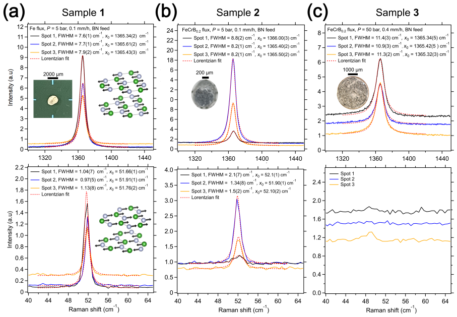
On its own terms, the paper's central claim is that TSFZ is a viable route to high-quality h-BN single crystals. The optimized procedure uses an Fe flux, a polycrystalline h-BN feed, moderate $N_2$ pressure ($P \approx 5$–$7$ bar), and a growth rate of 0.1 mm/h; the grown boules have diameters of 3–5 mm and lengths of 2–10 mm, with the largest crystalline grains reaching roughly 1 mm × 2 mm × 0.5 mm. X-ray diffraction, Raman spectroscopy, and photoluminescence show that the h-BN lattice itself is of high quality: the intralayer $E_{2g}$ mode has an average linewidth of 7.7(2) cm$^{-1}$ at 1365.46(4) cm$^{-1}$ and the interlayer shear mode 1.0(1) cm$^{-1}$ at 51.78(9) cm$^{-1}$, values comparable to CBF-grown crystals, and the PL spectrum has sharp phonon-assisted free-exciton peaks with minimal carbon-defect signal. The paper openly notes that the measured stacking-fault-to-exciton PL ratio (20.9, versus 2.4 and 1.1 for CBF samples) is higher, and that whether this is intrinsic to TSFZ or an artifact of cutting and polishing the samples is not yet settled.
Load-bearing premise
The paper assumes the high stacking-fault photoluminescence of its best sample is caused by cutting and polishing before measurement, not by the TSFZ growth itself; if the stacking faults are intrinsic, the claim that TSFZ matches CBF quality is unsupported.
Editorial extensions
If this is right
- Because TSFZ is continuous, it offers a path to bulk h-BN crystals larger than the roughly 1 mm by 100-micrometer plates typical of CBF growth.
- If the polishing explanation for the elevated stacking-fault PL is correct, polished TSFZ crystals would be expected to show CBF-comparable defect signals when measured on as-grown or cleaved surfaces.
- The lower 4.1 eV carbon-defect emission in the TSFZ sample than in a natural-isotope CBF sample suggests TSFZ's crucible-free geometry and zone refining reduce carbon contamination.
- Using a boron feed rod in TSFZ demonstrates that nitrogen can be supplied from the gas, which implies isotopic control of the grown h-BN is possible.
- The finding that Fe flux outperforms Fe-Cr in TSFZ, opposite to the trend in CBF, means flux chemistry interacts with growth geometry and needs separate optimization.
Reading between the lines
- If the stacking-fault excess is indeed polishing-induced, the practical payoff is large: TSFZ may already produce material whose intrinsic defect density matches CBF, and the technique's inherent scalability becomes the main remaining challenge.
- A direct way to test the paper's open question would be growing at 50 bar with the same 0.1 mm/h rate used at low pressure; the present 50 bar runs were limited to 0.4 mm/h, so pressure and rate effects are conflated.
- The occasional columnar, c-axis-oriented growth hints that, with the right seeding and interface control, TSFZ could grow thick h-BN ingots with an ideal shape for exfoliation, a form factor CBF cannot deliver.
- Because TSFZ can use either h-BN or boron feed rods, one could isotopically enrich or dope the feed to engineer the crystal's phonon and thermal properties.
Editorial analysis
A structured set of objections, weighed in public.
Referee Report
Summary. The paper reports the first demonstration of hexagonal BN (h-BN) crystal growth by the traveling-solvent floating-zone (TSFZ) method, using Fe or FeCr-based fluxes under N2 pressures of 1–50 bar. Boules 3–5 mm in diameter and 2–10 mm long were grown, with microCT showing grains up to roughly 1 mm × 2 mm × 0.5 mm and variable amounts of trapped flux. For the optimized growth (Fe flux, 5–7 bar, 0.1 mm/h), Raman spectroscopy gives an intralayer E2g linewidth of 7.7(2) cm−1 and an interlayer shear-mode linewidth of 1.0(1) cm−1, comparable to values reported for crucible-based flux (CBF) crystals; photoluminescence shows sharp phonon-assisted free-exciton features and strongly reduced carbon-related emission near 3.9–4.1 eV. The authors conclude that TSFZ is a viable route to larger, high-quality h-BN crystals.
Significance. If the feasibility result holds, this is a meaningful advance for bulk h-BN synthesis: TSFZ is crucible-free, offers zone-refining, and potentially enables larger crystals than the typical millimeter-scale CBF plates. The paper's strengths include the use of complementary characterization (microCT, powder and polished-surface XRD, SEM/EDS, Raman, PL), direct benchmarking against CBF crystals grown at Kansas State rather than only literature values, and unusually candid acknowledgment of unresolved issues, including flux inclusions, the pressure/rate confound, and the stacking-fault question. The central feasibility claim—that TSFZ can grow h-BN grains with Raman linewidths comparable to CBF material—is supported by the data. However, the stronger 'on par with, or superior to CBF' claim in the Conclusions rests on an untested assumption about the origin of the enhanced stacking-fault-related PL, and the evidence base for the optimized-growth comparison is a single boule.
major comments (3)
- [§5, Table 1, Fig. 6] The central quality benchmark for the optimized TSFZ material is the PL ratio PL(5.48 eV)/PL(5.77 eV) = 20.9 for sample 1, versus 2.4 and 1.1 for the CBF samples. The manuscript attributes this order-of-magnitude excess to cutting and polishing, citing the unpolished dendritic flake (sample 8, ratio 2.7) and deformation studies [73]. This control is not adequate: sample 8 was grown with a FeB0.2 flux rather than the optimized Fe flux and is a thin flake rather than a sectioned bulk boule, so it does not isolate the effect of polishing from the effect of growth conditions. Because the text itself states that 'the intrinsic stacking fault density characteristic of the TSFZ technique is currently unclear,' the claim in §6 that the optimized procedure yields crystals 'on par with, or superior to' CBF crystals in crystallinity is not yet supported. The authors should either provide a same-sample before/after polishing comparison on the optimized material or explicitly limit the quality claim to the Raman linewidth and carbon-defect PL results.
- [§6 Conclusions] The Conclusions state that TSFZ-grown h-BN is 'on par with, or superior to' CBF crystals 'in terms of purity and crystallinity,' but the PL data in §5 show that the TSFZ samples have significantly higher stacking-fault-related emission than the CBF samples, and the Discussion explicitly leaves open whether this is intrinsic. This is in tension with the statement in the same Conclusions that 'the TSFZ samples reported here mostly show higher stacking fault densities than reported CBF samples.' The crystallinity claim should be separated into (i) the intralayer Raman linewidth, which is supported by the data, and (ii) the stacking-fault density, which is unresolved.
- [§4 and §5, Table 1] The optimized-growth quality comparison rests on spectroscopy of a single boule (sample 1) for PL, and on a different, unpolished piece of the same boule for Raman. No replicate of the optimized Fe-flux, 5–7 bar, 0.1 mm/h growth is spectroscopically characterized. Given the large run-to-run variation visible in the microCT and Raman data across the other samples, the statement that the 'currently optimized growth procedure produces' crystals of this quality would be materially strengthened by a second optimized-growth sample. I do not consider this a fatal flaw for a feasibility demonstration, but it is part of the evidence needed for the 'on par' claim.
minor comments (4)
- [Abstract and Fig. 5a] The abstract and Introduction report the interlayer E2g FWHM as 1.0(1) cm−1, while the Fig. 5a caption reports 1.1(1) cm−1; please reconcile these values.
- [§5 Discussion] The sentence 'the intralayer mode is substantially broadened compared to samples 1 and 3' appears to be a typo; sample 3 is the sample with the broadened mode, so the comparison should presumably be to samples 1 and 2.
- [§4 Results] The phrase 'The signal corresponding signal in sample3 shows no resolvable peaks' contains a duplicated word.
- [Fig. 6b] The comparison in Fig. 6b would benefit from a legend or caption explicitly identifying which CBF sample has natural isotope abundance and which is isotopically enriched, since the text refers to both.
Circularity Check
No significant circularity: the feasibility claim rests on direct measurements, and quality benchmarks are external literature values and directly measured CBF samples, not quantities derived from the paper's own inputs.
full rationale
This is an experimental crystal-growth paper, not a derivation or fitting exercise. The central claim—that h-BN crystals can be grown by the TSFZ technique—is supported by X-ray tomography, XRD, SEM/EDS, Raman, and PL measurements reported directly in the paper, with no fitted parameter that is then renamed as a prediction. The quality benchmark comparison uses external literature values (Raman FWHM 7.6 cm-1 from an APHT Fe-flux CBF sample, 7.3 cm-1 from HPHT CBF, PL ratios 1.1 and 0.9 from literature) as well as CBF samples measured directly in the same study; these are independent evidence rather than outputs of the paper's own model. The one place where the paper makes an interpretive assumption—the high PL(5.48 eV)/PL(5.77 eV) ratio of 20.9 in the polished TSFZ sample—is explicitly flagged as possibly extrinsic, with the authors stating that 'the intrinsic stacking fault density characteristic of the TSFZ technique is currently unclear' and citing an external deformation study (Watanabe et al., ref. [73]) for the physical mechanism. That is an admitted uncertainty about an assumption, not a circular derivation. Self-citations are present (e.g., refs. [53, 54] for the high-pressure floating-zone furnace and ref. [4] for the indirect-gap assignment), but they are methodological or background references and are not load-bearing for the central claim. No equation in the paper reduces to another equation by construction, and no fitted input is relabeled as a prediction. The appropriate finding is no significant circularity.
Assumptions & free parameters
assumptions (3)
- domain assumption Raman FWHM of the E2g intralayer mode is a valid transferable metric of h-BN crystallinity.
- domain assumption PL peaks at 3.9 and 4.1 eV are carbon-related defects, and sharp phonon-assisted free-exciton peaks indicate high purity.
- domain assumption Sieverts' law applies to nitrogen solubility in the Fe flux, so N2 partial pressure controls nitrogen activity.
Cite this review
Pith. "Pith review of Growth of hexagonal BN crystals by traveling-solvent floating zone." pith.science (2026). https://pith.science/paper/NRRDEHXD
@misc{pith2026241217195,
  author       = {Pith},
  title        = {Pith review of: Growth of hexagonal BN crystals by traveling-solvent floating zone},
  year         = {2026},
  howpublished = {\url{https://pith.science/paper/NRRDEHXD}},
  note         = {Machine review of arXiv:2412.17195}
}
abstract
Large, high-purity single-crystals of hexagonal BN (h-BN) are essential for exploiting its many desirable and interesting properties. Here, we demonstrate via X-ray tomography, X-ray diffraction and scanning electron microscopy that h-BN crystals can be grown by traveling-solvent floating-zone (TSFZ). The diameters of grown boules range from 3 - 5 mm with lengths from 2 - 10 mm. Tomography indicates variable grain sizes within the boules, with the largest having areas of $\approx$ 1 mm $\times$ 2 mm and thickness $\approx$ 0.5 mm. Although the boules contain macroscale flux inclusions, the h-BN lattice itself is of high quality for samples grown under optimized conditions. The currently optimized growth procedure employs an Fe flux, moderate N$_2$ pressure ($P_{N2} \approx$ 6 bar), and a growth rate of 0.1 mm/h. Raman spectroscopy for an optimized sample gives an average linewidth of 7.7(2) cm$^{-1}$ for the E$_{\mathrm{2g}}$ intralayer mode at 1365.46(4) cm$^{-1}$ and 1.0(1) cm$^{-1}$ for the E$_{\mathrm{2g}}$ interlayer shear mode at 51.78(9) cm$^{-1}$. The corresponding photoluminescence spectrum shows sharp phonon-assisted free exciton peaks and minimal signal in the energy range corresponding to carbon-related defects ($E$ = 3.9 4.1 eV). Our work demonstrates the viability of growing h-BN by the TSFZ technique, thereby opening a new route towards larger, high-quality crystals and advancing the state of h-BN related research.
Figures


Figures from the paper (2 more)

Reference graph
Works this paper leans on
-
[73]
Band-edge luminescence of deformed hexagonal boron nitride single crystals
Watanabe,K.,Taniguchi,T.,Kuroda,T.,Kanda,H.,2006. Band-edge luminescence of deformed hexagonal boron nitride single crystals. Diamond Relat. Mater. 15, 1891–1893. doi:10.1016/j.diamond.2006. 06.014
-
[1]
Electric field effectinatomicallythincarbonfilms
Novoselov, K.S., Geim, A.K., Morozov, S.V., Jiang, D., Zhang, Y., Dubonos, S.V., Grigorieva, I.V., Firsov, A.A., 2004. Electric field effectinatomicallythincarbonfilms. Science306,666–669. doi: 10. 1126/science.1102896
2004
-
[2]
Two-dimensional atomic crys- tals
Novoselov, K.S., Jiang, D., Schedin, F., Booth, T., Khotkevich, V., Morozov, S., Geim, A.K., 2005. Two-dimensional atomic crys- tals. Proc. Natl. Acad. Sci. 102, 10451–10453. doi:10.1073/pnas. 0502848102
doi:10.1073/pnas 2005
-
[3]
Boron nitride substrates for high-quality graphene electronics
Dean, C.R., Young, A.F., Meric, I., Lee, C., Wang, L., Sorgenfrei, S., Watanabe, K., Taniguchi, T., Kim, P., Shepard, K.L., et al., 2010. Boron nitride substrates for high-quality graphene electronics. Nat. Nanotechnol. 5, 722–726. doi:10.1038/NNANO.2010.172
-
[4]
Hexagonal boron nitride is an indirect bandgap semiconductor
Cassabois, G., Valvin, P., Gil, B., 2016. Hexagonal boron nitride is an indirect bandgap semiconductor. Nat. Photon. 10, 262–266. doi:10.1038/nphoton.2015.277
-
[5]
Modulating the thermal conductivity inhexagonalboronnitrideviacontrolledboronisotopeconcentration
Yuan, C., Li, J., Lindsay, L., Cherns, D., Pomeroy, J.W., Liu, S., Edgar, J.H., Kuball, M., 2019. Modulating the thermal conductivity inhexagonalboronnitrideviacontrolledboronisotopeconcentration. Commun. Phys. 2, 43. doi:10.1038/s42005-019-0145-5
-
[6]
Hexagonal boron nitride: a promising substrate for graphene with high heat dissipation
Zhang, Z., Hu, S., Chen, J., Li, B., 2017. Hexagonal boron nitride: a promising substrate for graphene with high heat dissipation. Nan- otechnology 28, 225704. doi:10.1088/1361-6528/aa6e49
-
[7]
Ultrathin high- temperature oxidation-resistant coatings of hexagonal boron nitride
Liu, Z., Gong, Y., Zhou, W., Ma, L., Yu, J., Idrobo, J.C., Jung, J., MacDonald, A.H., Vajtai, R., Lou, J., et al., 2013. Ultrathin high- temperature oxidation-resistant coatings of hexagonal boron nitride. Nat. Commun. 4, 2541. doi:10.1038/ncomms3541
Show all 82 references
-
[8]
Šiškins, M., Mullan, C., Son, S.K., Yin, J., Watanabe, K., Taniguchi, T., Ghazaryan, D., Novoselov, K.S., Mishchenko, A.,
-
[9]
Signatures oftunablesuperconductivityinatrilayergraphenemoirésuperlattice
Chen,G.,Sharpe,A.L.,Gallagher,P.,Rosen,I.T.,Fox,E.J.,Jiang,L., Lyu,B.,Li,H.,Watanabe,K.,Taniguchi,T.,etal.,2019a. Signatures oftunablesuperconductivityinatrilayergraphenemoirésuperlattice. Nature 572, 215–219. doi:10.1038/s41586-019-1393-y
-
[10]
Evidence of a gate- tunable Mott insulator in a trilayer graphene moiré superlattice
Chen,G.,Jiang,L.,Wu,S.,Lyu,B.,Li,H.,Chittari,B.L.,Watanabe, K., Taniguchi, T., Shi, Z., Jung, J., et al., 2019b. Evidence of a gate- tunable Mott insulator in a trilayer graphene moiré superlattice. Nat. Phys. 15, 237–241. doi:10.1038/s41567-018-0387-2
-
[11]
Gate-dependentpseudospin mixing in graphene/boron nitride moiré superlattices
Shi, Z., Jin, C., Yang, W., Ju, L., Horng, J., Lu, X., Bechtel, H.A., Martin,M.C.,Fu,D.,Wu,J.,etal.,2014. Gate-dependentpseudospin mixing in graphene/boron nitride moiré superlattices. Nat. Phys. 10, 743–747. doi:10.1038/nphys3075
2014 doi
-
[12]
Ponomarenko, L., Gorbachev, R., Yu, G., Elias, D., Jalil, R., Patel, A., Mishchenko, A., Mayorov, A., Woods, C., Wallbank, J., et al.,
-
[13]
Boron nitride for excitonics, nanophotonics, and quantum technologies
Gil,B.,Cassabois,G.,Cusco,R.,Fugallo,G.,Artus,L.,2020. Boron nitride for excitonics, nanophotonics, and quantum technologies. Nanophotonics 9, 3483–3504. doi:10.1515/nanoph-2020-0225
2020 doi
-
[14]
Structure,propertiesandapplicationsoftwo-dimensional hexagonalboronnitride
Roy,S.,Zhang,X.,Puthirath,A.B.,Meiyazhagan,A.,Bhattacharyya, S., Rahman, M.M., Babu, G., Susarla, S., Saju, S.K., Tran, M.K., etal.,2021. Structure,propertiesandapplicationsoftwo-dimensional hexagonalboronnitride. Adv.Mater.33,2101589. doi: 10.1002/adma. 202101589
2021 doi
-
[15]
Recent development of boron nitride towards electronic applications
Izyumskaya, N., Demchenko, D.O., Das, S., Özgür, Ü., Avrutin, V., Morkoç, H., 2017. Recent development of boron nitride towards electronic applications. Adv. Electron. Mater. 3, 1600485. doi:10. 1002/aelm.201600485
2017
-
[16]
Quan- tumsensingandimagingwithspindefectsinhexagonalboronnitride
Vaidya, S., Gao, X., Dikshit, S., Aharonovich, I., Li, T., 2023. Quan- tumsensingandimagingwithspindefectsinhexagonalboronnitride. Adv. Phys.: X 8, 2206049. doi:10.1080/23746149.2023.2206049
2023
-
[17]
Photonics with hexagonal boron nitride
Caldwell, J.D., Aharonovich, I., Cassabois, G., Edgar, J.H., Gil, B., Basov, D., 2019. Photonics with hexagonal boron nitride. Nat. Rev. Mater. 4, 552–567. doi:10.1038/s41578-019-0124-1
2019 doi
-
[18]
Tunable phonon polaritons in atomically thin Van der Waals crystals of boron nitride
Dai,S.,Fei,Z.,Ma,Q.,Rodin,A.,Wagner,M.,McLeod,A.,Liu,M., Gannett, W., Regan, W., Watanabe, K., et al., 2014. Tunable phonon polaritons in atomically thin Van der Waals crystals of boron nitride. Science 343, 1125–1129. doi:10.1126/science.1246833
2014 doi
-
[19]
Quantum emission from hexagonal boron nitride monolayers
Tran, T.T., Bray, K., Ford, M.J., Toth, M., Aharonovich, I., 2016. Quantum emission from hexagonal boron nitride monolayers. Nat. Nanotech. 11, 37–41. doi:10.1038/nnano.2015.242
2016 doi
-
[20]
Bright UV single photon emission at point defects in h-BN
Bourrellier, R., Meuret, S., Tararan, A., Stéphan, O., Kociak, M., Tizei, L.H., Zobelli, A., 2016. Bright UV single photon emission at point defects in h-BN. Nano Lett. 16, 4317–4321. doi:10.1021/acs. nanolett.6b01368
2016 doi
-
[21]
Fournier,C.,Plaud,A.,Roux,S.,Pierret,A.,Rosticher,M.,Watanabe, K.,Taniguchi,T.,Buil,S.,Quélin,X.,Barjon,J.,etal.,2021.Position- controlled quantum emitters with reproducible emission wavelength in hexagonal boron nitride. Nat. Commun. 12, 3779. doi:10.1038/ s41467-021-24019-6
2021
-
[22]
Single-photon sources
Lounis, B., Orrit, M., 2005. Single-photon sources. Rep. Prog. Phys. 68, 1129. doi:10.1088/0034-4885/68/5/R04
2005 doi
-
[23]
High-resolution optical imaging and sensing using quantumemittersinhexagonalboron-nitride
Bradac, C., 2021. High-resolution optical imaging and sensing using quantumemittersinhexagonalboron-nitride. Front.Phys.9,641341. doi:10.3389/fphy.2021.641341
2021
-
[24]
Strain quantum sensing with spin defects in hexagonal boron nitride
Lyu, X., Tan, Q., Wu, L., Zhang, C., Zhang, Z., Mu, Z., Zúñiga- Pérez, J., Cai, H., Gao, W., 2022. Strain quantum sensing with spin defects in hexagonal boron nitride. Nano Lett. 22, 6553–6559. doi:10.1021/acs.nanolett.2c01722
2022 doi
-
[25]
A planar defect spin sensorinatwo-dimensionalmaterialsusceptibletostrainandelectric fields
Udvarhelyi, P., Clua-Provost, T., Durand, A., Li, J., Edgar, J.H., Gil, B., Cassabois, G., Jacques, V., Gali, A., 2023. A planar defect spin sensorinatwo-dimensionalmaterialsusceptibletostrainandelectric fields. npj Comput. Mater. 9, 150. doi:10.1038/s41524-023-01111-7
2023 doi
-
[26]
Dahal, R., Li, J., Majety, S., Pantha, B.N., Cao, X., Lin, J., Jiang, H.,
-
[27]
Epitaxial single- crystal hexagonal boron nitride multilayers on Ni (111)
Ma,K.Y.,Zhang,L.,Jin,S.,Wang,Y.,Yoon,S.I.,Hwang,H.,Oh,J., Jeong, D.S., Wang, M., Chatterjee, S., et al., 2022. Epitaxial single- crystal hexagonal boron nitride multilayers on Ni (111). Nature 606, 88–93. doi:10.1038/s41586-022-04745-7. : Preprint submitted to Elsevier Page 12 of 14
2022 doi
-
[28]
Ultraflat single- crystal hexagonal boron nitride for wafer-scale integration of a 2D- compatible high-𝜅 metal gate
Wang, Y., Zhao, C., Gao, X., Zheng, L., Qian, J., Gao, X., Li, J., Tang, J., Tan, C., Wang, J., et al., 2024. Ultraflat single- crystal hexagonal boron nitride for wafer-scale integration of a 2D- compatible high-𝜅 metal gate. Nat. Mater. 23, 1495–1501. doi:10. 1038/s41563-024-01968-z
2024
-
[29]
Wafer- scalesingle-crystalhexagonalboronnitridemonolayersonCu(111)
Chen, T.A., Chuu, C.P., Tseng, C.C., Wen, C.K., Wong, H.S.P., Pan, S., Li, R., Chao, T.A., Chueh, W.C., Zhang, Y., et al., 2020. Wafer- scalesingle-crystalhexagonalboronnitridemonolayersonCu(111). Nature 579, 219–223. doi:10.1038/s41586-020-2009-2
2020 doi
-
[30]
Large-area synthesis and transfer of multilayer hexagonal boron nitride for enhanced graphene device arrays
Fukamachi,S.,Solís-Fernández,P.,Kawahara,K.,Tanaka,D.,Otake, T., Lin, Y.C., Suenaga, K., Ago, H., 2023. Large-area synthesis and transfer of multilayer hexagonal boron nitride for enhanced graphene device arrays. Nat. Electron. 6, 126–136. doi: 10.1038/ s41928-022-00911-x
2023
-
[31]
Rhombohedral and turbostratic boron nitride: X-ray diffraction and photoluminescencesignatures.Appl.Phys.Lett.119,262102.doi: 10
Moret, M., Rousseau, A., Valvin, P., Sharma, S., Souqui, L., Peder- sen, H., Högberg, H., Cassabois, G., Li, J., Edgar, J., et al., 2021. Rhombohedral and turbostratic boron nitride: X-ray diffraction and photoluminescencesignatures.Appl.Phys.Lett.119,262102.doi: 10. 1063/5.0076424
2021
-
[32]
Page,R.,Casamento,J.,Cho,Y.,Rouvimov,S.,Xing,H.G.,Jena,D.,
-
[33]
Tsai,C.,Kobayashi,Y.,Akasaka,T.,Kasu,M.,2009.Molecularbeam epitaxial growth of hexagonal boron nitride on Ni (111) substrate. J. Cryst.Growth311,3054–3057. doi: 10.1016/j.jcrysgro.2009.01.077
2009 doi
-
[34]
Vuong, T., Cassabois, G., Valvin, P., Rousseau, E., Summerfield, A., Mellor, C., Cho, Y., Cheng, T., Albar, J.D., Eaves, L., et al.,
-
[35]
High-temperature molecular beam epitaxy of hexagonal boron nitride with high active nitrogen fluxes
Cheng,T.S.,Summerfield,A.,Mellor,C.J.,Khlobystov,A.N.,Eaves, L., Foxon, C.T., Beton, P.H., Novikov, S.V., 2018. High-temperature molecular beam epitaxy of hexagonal boron nitride with high active nitrogen fluxes. Materials 11, 1119. doi:10.3390/ma11071119
2018 doi
-
[36]
Rotationally aligned hexagonal boron nitride on sapphire by high-temperature molecular beam epitaxy. Phys. Rev. Materials 3, 064001. doi:10.1103/PhysRevMaterials.3.064001
-
[37]
Alemoush, Z., Tingsuwatit, A., Maity, A., Li, J., Lin, J., Jiang, H.,
-
[38]
Synthesis of high-purity boron nitride single crystals under high pressure by using Ba–BN solvent
Taniguchi, T., Watanabe, K., 2007. Synthesis of high-purity boron nitride single crystals under high pressure by using Ba–BN solvent. J. Cryst. Growth 303, 525–529. doi:10.1016/j.jcrysgro.2006.12.061
2007 doi
-
[39]
Hexagonal boron nitride single crystal growth at atmospheric pressure using Ni- Cr solvent
Kubota,Y.,Watanabe,K.,Tsuda,O.,Taniguchi,T.,2008. Hexagonal boron nitride single crystal growth at atmospheric pressure using Ni- Cr solvent. Chem. Mater. 20, 1661–1663. doi:10.1021/cm7028382
2008 doi
-
[40]
Liu, S., He, R., Ye, Z., Du, X., Lin, J., Jiang, H., Liu, B., Edgar, J.H.,
-
[41]
Effect of growth temperature on the structural and optical properties of few-layer hexagonal boron nitride by molecular beam epitaxy
Laleyan, D.A., Mengle, K., Zhao, S., Wang, Y., Kioupakis, E., Mi, Z., 2018. Effect of growth temperature on the structural and optical properties of few-layer hexagonal boron nitride by molecular beam epitaxy. Opt. Express 26, 23031–23039. doi:10.1364/OE.26.023031
2018 doi
-
[42]
Zhang,S.Y.,Xu,K.,Zhao,X.K.,Shao,Z.Y.,Wan,N.,2019.Improved hBN single-crystal growth by adding carbon in the metal flux. Cryst. Growth Des. 19, 6252–6257. doi:10.1021/acs.cgd.9b00712
2019 doi
-
[43]
Hexagonal boron nitride single crystal growth from solution with a temperature gradient
Li, J., Yuan, C., Elias, C., Wang, J., Zhang, X., Ye, G., Huang, C., Kuball, M., Eda, G., Redwing, J.M., et al., 2020a. Hexagonal boron nitride single crystal growth from solution with a temperature gradient. Chem. Mater. 32, 5066–5072. doi:10.1021/acs.chemmater. 0c00830
-
[44]
Single crystal growth of monoisotopic hexagonal boron nitride from a Fe–Cr flux
Li, J., Elias, C., Ye, G., Evans, D., Liu, S., He, R., Cassabois, G., Gil, B., Valvin, P., Liu, B., et al., 2020b. Single crystal growth of monoisotopic hexagonal boron nitride from a Fe–Cr flux. J. Mater. Chem. C 8, 9931–9935. doi:10.1039/D0TC02143A
-
[45]
Hexagonal boron nitridecrystalgrowthfromiron,asinglecomponentflux
Li, J., Wang, J., Zhang, X., Elias, C., Ye, G., Evans, D., Eda, G., Redwing, J.M., Cassabois, G., Gil, B., et al., 2021. Hexagonal boron nitridecrystalgrowthfromiron,asinglecomponentflux. ACSNano 15, 7032–7039. doi:10.1021/acsnano.1c00115
2021 doi
-
[46]
In- fraredhyperbolicmetasurfacebasedonnanostructuredVanderWaals materials
Li,P.,Dolado,I.,Alfaro-Mozaz,F.J.,Casanova,F.,Hueso,L.E.,Liu, S., Edgar, J.H., Nikitin, A.Y., Vélez, S., Hillenbrand, R., 2018. In- fraredhyperbolicmetasurfacebasedonnanostructuredVanderWaals materials. Science 359, 892–896. doi:10.1126/science.aaq1704
2018 doi
-
[47]
Large-scale growth of high-quality hexagonal boron nitride crystals at atmospheric pressure from an Fe–Cr flux. Cryst. Growth Des. 17, 4932–4935. doi:10.1021/acs.cgd.7b00871
-
[48]
Liu,S.,He,R.,Xue,L.,Li,J.,Liu,B.,Edgar,J.H.,2018.Singlecrystal growth of millimeter-sized monoisotopic hexagonal boron nitride. Chem. Mater. 30, 6222–6225. doi:10.1021/acs.chemmater.8b02589
2018 doi
-
[49]
Fault-tolerant quantum computation by anyons
Kitaev, A., 2003. Fault-tolerant quantum computation by anyons. Ann. Phys. 303, 2–30. doi:10.1016/S0003-4916(02)00018-0
2003 doi
-
[50]
Disorder in Van der Waals heterostructures of 2D materials
Rhodes, D., Chae, S.H., Ribeiro-Palau, R., Hone, J., 2019. Disorder in Van der Waals heterostructures of 2D materials. Nat. Mater. 18, 541–549. doi:10.1038/s41563-019-0366-8
2019 doi
-
[51]
Hexagonal boron nitride synthe- sized at atmospheric pressure using metal alloy solvents: evaluation asasubstratefor2Dmaterials
Onodera, M., Taniguchi, T., Watanabe, K., Isayama, M., Masubuchi, S., Moriya, R., Machida, T., 2019. Hexagonal boron nitride synthe- sized at atmospheric pressure using metal alloy solvents: evaluation asasubstratefor2Dmaterials. NanoLett.20,735–740. doi: 10.1021/ acs.nanolett.9b04641
2019
-
[52]
Techniques of zone melting and crystal growing
Pfann, W., 1957. Techniques of zone melting and crystal growing. Solid State Phys. 4, 423–521. doi:10.1016/S0081-1947(08)60158-7
1957 doi
-
[53]
High- pressure laser floating zone furnace
Schmehr, J.L., Aling, M., Zoghlin, E., Wilson, S.D., 2019. High- pressure laser floating zone furnace. Rev. Sci. Instrum. 90. doi:10. 1063/1.5085327
2019
-
[54]
Ultralow-losspolaritonsinisotopicallypureboronnitride.Nat.Mater
Giles, A.J., Dai, S., Vurgaftman, I., Hoffman, T., Liu, S., Lindsay, L., Ellis, C.T., Assefa, N., Chatzakis, I., Reinecke, T.L., et al., 2018. Ultralow-losspolaritonsinisotopicallypureboronnitride.Nat.Mater. 17, 134–139. doi:10.1038/nmat5047
2018 doi
-
[55]
Anyons in an exactly solved model and beyond
Kitaev, A., 2006. Anyons in an exactly solved model and beyond. Ann. Phys. 321, 2–111. doi:10.1016/j.aop.2005.10.005
2006 doi
-
[56]
Laser-heated pedestal growth of oxide fibers
Andreeta, M.R., Hernandes, A.C., 2010. Laser-heated pedestal growth of oxide fibers. Springer, Berlin, Heidelberg. pp. 393–432. doi:10.1007/978-3-540-74761-1_13
2010 doi
-
[57]
Iron—Binary phase diagrams
Kubaschewski, O., 2013. Iron—Binary phase diagrams. Springer Science & Business Media
2013
-
[58]
NRecon Reconstruction Soft- ware
MicroPhotonics, 2020. NRecon Reconstruction Soft- ware. https://www.microphotonics.com/micro-ct-systems/ nrecon-reconstruction-software/. Accessed: 2024-10-29
2020
-
[59]
Geick,R.,Perry,C.,Rupprecht,G.,1966.Normalmodesinhexagonal boron nitride. Phys. Rev. 146, 543. doi:10.1103/PhysRev.146.543
1966 doi
-
[60]
Defect-related photo- luminescence of hexagonal boron nitride
Museur, L., Feldbach, E., Kanaev, A., 2008. Defect-related photo- luminescence of hexagonal boron nitride. Phys. Rev. B 78, 155204. doi:10.1103/PhysRevB.78.155204
2008 doi
-
[61]
Advances in high-pressure laser floating zone growth: The Laser Optical Kristallmacher II (LOKII)
GomezAlvarado,S.J.,Zoghlin,E.,Jackson,A.,Kautzsch,L.,Plumb, J., Aling, M., Capa Salinas, A.N., Pokharel, G., Pang, Y., Gomez, R.M., et al., 2024. Advances in high-pressure laser floating zone growth: The Laser Optical Kristallmacher II (LOKII). Rev. Sci. Instrum. 95. doi:10.10...
2024 doi
-
[62]
Feigelson, R., 1985. The laser-heated pedestal growth method: a powerful tool in the search for new high performance laser crystals, in: Tunable Solid State Lasers: Proceedings of the First International ConferenceLaJolla,Calif.,June13–15,1984,Springer.pp.129–142. doi:10.1007/...
1985 doi
-
[63]
Point defects in hexagonalboronnitride.I.EPR,thermoluminescence,andthermally- stimulated-current measurements
Katzir, A., Suss, J., Zunger, A., Halperin, A., 1975. Point defects in hexagonalboronnitride.I.EPR,thermoluminescence,andthermally- stimulated-current measurements. Phys. Rev. B 11, 2370. doi:10. 1103/PhysRevB.11.2370
1975
-
[64]
arXiv preprint arXiv:2405.20837 doi:10.48550/arXiv.2405.20837
Plo,J.,Pershin,A.,Li,S.,Poirier,T.,Janzen,E.,Schutte,H.,Tian,M., Wynn,M.,Bernard,S.,Rousseau,A.,etal.,2024.Isotopesubstitution and polytype control for point defects identification: the case of the ultraviolet color center in hexagonal boron nitride. arXiv preprint arXiv:2405....
-
[65]
Phase diagrams of ternary iron alloys
Raghavan, V., 1987. Phase diagrams of ternary iron alloys. ASM International
1987
-
[66]
Reviewofthermodynamicproperties of the Cr-N system
DeLuca,J.,Leitnaker,J.,1973. Reviewofthermodynamicproperties of the Cr-N system. J. Am. Chem. Soc. 56, 126–129. doi:10.1111/j. 1151-2916.1973.tb15426.x
1973
-
[67]
AthermodynamicevaluationoftheCr-Fe-Nsystem
Frisk,K.,1990. AthermodynamicevaluationoftheCr-Fe-Nsystem. Metall. Trans. A 21, 2477–2488. doi:10.1007/BF02646992
1990 doi
-
[68]
Near band-gap photoluminescence properties of hexagonal boron nitride
Museur, L., Kanaev, A., 2008. Near band-gap photoluminescence properties of hexagonal boron nitride. J. Appl. Phys. 103, 103520. doi:10.1063/1.2925685
2008 doi
-
[69]
Electronspinresonanceincarbon-doped boron nitride
Moore,A.,Singer,L.,1972. Electronspinresonanceincarbon-doped boron nitride. J. Phys. Chem. Solids 33, 343–356. doi: 10.1016/ 0022-3697(72)90016-9
1972
-
[70]
Compound Semiconductor 30, 46–50
Sadovyi,B.,Sadovyi,P.,Porowski,S.,Grzegory,I.,2024b.Producing high-quality hexagonal BN. Compound Semiconductor 30, 46–50
-
[71]
OptimizationofNi–Crfluxgrowthforhexagonalboronnitridesingle crystals
Hoffman, T.B., Clubine, B., Zhang, Y., Snow, K., Edgar, J.H., 2014. OptimizationofNi–Crfluxgrowthforhexagonalboronnitridesingle crystals. J. Cryst. Growth 393, 114–118. doi:10.1016/j.jcrysgro. 2013.09.030
2014 doi
-
[72]
Isotopeengineering ofVanderWaalsinteractionsinhexagonalboronnitride
Vuong, T., Liu, S., Van der Lee, A., Cuscó, R., Artús, L., Michel, T., Valvin,P.,Edgar,J.,Cassabois,G.,Gil,B.,2018. Isotopeengineering ofVanderWaalsinteractionsinhexagonalboronnitride. Nat.Mater. 17, 152–158. doi:10.1038/nmat5048
2018 doi
-
[74]
Characterization methods dedicated to nanometer-thick hBN layers
Schué, L., Stenger, I., Fossard, F., Loiseau, A., Barjon, J., 2016. Characterization methods dedicated to nanometer-thick hBN layers. 2D Materials 4, 015028
2016
-
[75]
Absorption of gases by metals
Sieverts, A., 1929. Absorption of gases by metals. Zeitschrift für Metallkunde 21, 37–46
1929
-
[76]
Comparative evaluation of h-BN crystals properties grown under high N2 pressure with pure Ni and Ni–Crsolventsviathermalgradienttechnique
Sadovyi, P., Nikolenko, B., Strelchuk, V., Turko, B., Petrusha, I., Porowski, S., Grzegory, I., 2024a. Comparative evaluation of h-BN crystals properties grown under high N2 pressure with pure Ni and Ni–Crsolventsviathermalgradienttechnique. E-MRSFallMeeting, Symposium P: Boro...
-
[82]
Watanabe,K.,Taniguchi,T.,2009.Jahn-Tellereffectonexcitonstates in hexagonal boron nitride single crystal. Phys. Rev. B 79, 193104. : Preprint submitted to Elsevier Page 14 of 14
2009
-
[2011]
Epitaxially grown semiconducting hexagonal boron nitride as a deep ultraviolet photonic material. Appl. Phys. Lett. 98, 211110. doi:10.1063/1.3593958
-
[2013]
Nature 497, 594–597
Cloning of Dirac fermions in graphene superlattices. Nature 497, 594–597. doi:10.1038/nature12187
-
[2017]
2D Mater
Deep ultraviolet emission in hexagonal boron nitride grown by high-temperature molecular beam epitaxy. 2D Mater. 4, 021023. doi:10.1088/2053-1583/aa604a
-
[2019]
High-temperature electronic devices enabled by hBN- encapsulated graphene. Appl. Phys. Lett. 114, 123104. doi:10.1063/ 1.5088587
-
[2024]
Status of h-BN quasi-bulk crystals and high efficiency neutron detectors. J. Appl. Phys. 135, 175704. doi:10.1063/5.0179610
Reviewed August 11, 2026 · model on record in the stance chip above.
Discussion (0). Continue with ORCID to comment.