REVIEW 3 major objections 6 minor 33 references
Graphene intercalation of the large gap quantum spin Hall insulator bismuthene
T0 review · 3 major / 6 minor · reviewed 2026-08-09 · deepseek-v4-flash
Pith's one-line read Graphene intercalation preserves the topological state of bismuthene and shields it from oxidation in air.
desk verdict Convincing intercalation and oxidation protection; the topological gap claim is indirect but the circumstantial case is strong. read the letter →
The pith
A machine-rendered reading of the paper's core claim, the machinery that carries it, and where it could break.
The reading
What carries the argument
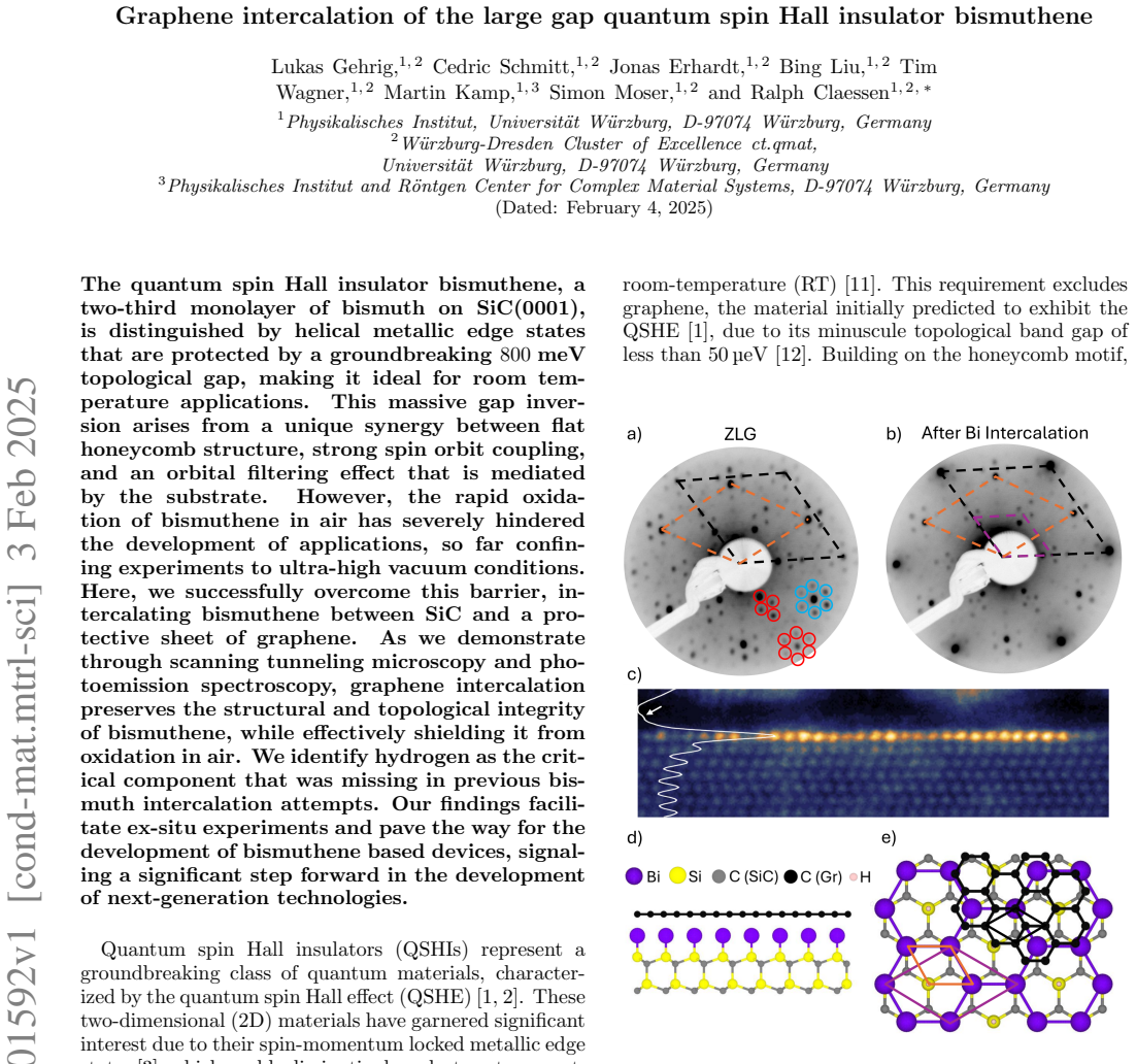
The key object is bismuthene, the two-thirds monolayer bismuth phase on SiC(0001), a (√3×√3)R30° superstructure whose flat honeycomb geometry, strong spin-orbit coupling, and substrate-mediated orbital filtering open an 800 meV topological gap. The enabling step in this work is hydrogen-assisted intercalation: annealing with hydrogen passivates the silicon dangling bonds and decouples the graphene overlayer, and a final 550 °C desorption drives the bismuth coverage to the 2/3 monolayer phase rather than the 1/3 or full-monolayer structures seen in earlier attempts. The evidence chain then rests on four measurements: LEED/STEM for the atomic registry, STM for the moiré pattern and edge modulations, ARPES plus potassium doping for the band structure and gap lower bound, and XPS for oxidation resistance.
What would settle it
Measure nonlocal or two-terminal transport through the buried edge channels at room temperature: quantized helical edge conductance that persists after air exposure would confirm the preserved topological phase, while a bulk-dominated conductivity or the complete absence of edge conductance would show that the STM modulation and 230 meV lower bound were not sufficient evidence.
Extended reading notes
Core claim
The authors claim to stabilize the 2/3 monolayer bismuthene phase as an intercalant between 4H-SiC(0001) and zero-layer graphene. After depositing bismuth and annealing at 350 °C, a subsequent desorption at 550 °C in a hydrogen atmosphere removes excess bismuth and leaves a single bismuth layer sitting at the T1 sites directly above silicon, in the same (√3×√3)R30° arrangement as pristine bismuthene. LEED and cross-sectional STEM confirm the vertical stacking; STM resolves both the graphene overlayer and the bismuthene lattice, together with a moiré pattern of about 3.2 nm. ARPES shows the characteristic px/py bands of bismuthene, matching density functional calculations for the pristine phase, and potassium doping saturates the valence band at about –230 meV below the Fermi level, giving a conservative lower bound for the preserved topological gap. STM at SiC step edges shows the same enhanced signal and √3 modulation seen at pristine bismuthene edges, which the authors interpret as conserved topological edge states. XPS shows that the Bi 4f core levels remain unchanged after exposure to oxygen and ambient air, unlike the pristine, uncapped film, which develops oxidation satellites.
Load-bearing premise
The load-bearing assumption is that the valence-band stop at about 230 meV below the Fermi energy gives a true lower bound for the topological gap, and that the √3-periodic bright lines seen at silicon-carbide step edges belong to helical topological edge states; if either signal is actually a trivial edge effect or a potassium-doping artifact, the claim that bismuthene's topological order survives the graphene cap is not proven.
Editorial extensions
If this is right
- The 2/3 monolayer bismuthene phase can be intercalated beneath one graphene sheet on SiC(0001), giving a buried quantum spin Hall insulator with the same (√3×√3)R30° registry as the pristine film.
- The preserved valence-band saturation at about –230 meV places the topological gap at or above room-temperature requirements, so the buried edge states should survive thermal excitation.
- The graphene cap blocks oxidation of bismuthene in oxygen and ambient air, so samples grown in ultrahigh vacuum can be taken out for ex situ experiments and device processing.
- The hydrogen desorption step is the decisive control that selects the 2/3 monolayer phase instead of the metallic or 1/3 monolayer trivial films reported in earlier intercalation attempts.
Reading between the lines
- Extending this result, one could map the bismuth phase diagram against hydrogen partial pressure and annealing time; the paper identifies hydrogen as the missing ingredient but does not show how sharp the 2/3 monolayer window is.
- Because the finished stack has n-doped graphene and p-doped bismuthene, it behaves as a built-in heterojunction; gating the stack would let one tune the relative doping, possibly reaching bismuthene charge neutrality without potassium deposition.
- The edge-state evidence here is topographic rather than transport-based; a direct nonlocal conductance measurement through the buried helical edge would test topological protection more stringently than STM modulation alone.
Signed reviews
Editorial analysis
A structured set of objections, weighed in public.
Referee Report
Summary. This manuscript reports an intercalation protocol that places the 2/3-monolayer bismuthene phase between SiC(0001) and an epitaxial graphene overlayer. The structural identity of the intercalated film is established through LEED, cross-sectional STEM, and bias-dependent STM, and the valence band is compared with literature DFT calculations. Potassium dosing in ARPES is used to infer a 230 meV lower bound for the band gap from saturation of the bismuthene valence band, and STM images at SiC step edges are presented as evidence for conserved topological edge states. Finally, XPS shows that the graphene cap suppresses bismuth oxidation upon oxygen and air exposure. The authors conclude that graphene intercalation preserves the structural and topological integrity of bismuthene while making it air-stable.
Significance. The structural intercalation and air-stability results are well supported and practically valuable: the hydrogen-assisted protocol appears to solve a previously elusive preparation problem, and the XPS comparison between pristine and capped bismuthene directly demonstrates oxidation protection. The paper also benefits from comparison with independent literature DFT calculations rather than fitting its own model, and the LEED/STEM/STM evidence for the 2/3-monolayer phase is convincing. The main weakness is that the topological-integrity claim rests on an indirect gap estimate and on edge-state signatures that are not unique; those parts of the argument need strengthening or explicit reframing.
major comments (3)
- [Fig. 4 and accompanying text] The inference that valence-band saturation at about -230 meV gives Egap >= 230 meV assumes that potassium electrons are transferred into the bismuthene conduction band and that no in-gap states pin the Fermi level. The conduction band is never observed, so the identical ARPES signature would arise from a trivial 230 meV gap, from a defect-pinned Fermi level, or from a potassium-induced electrostatic shift. The non-dispersive K 4s feature at -760 meV in Fig. 4c shows that K-derived states are occupied near the valence band, so the simple rigid-band charge-transfer picture is not established. Please either provide direct evidence of conduction-band occupation or spin texture, or explicitly state the assumptions under which the 230 meV value is a valid lower bound.
- [Fig. 5 and surrounding text] The enhanced tunneling signal with sqrt(3) periodicity at SiC step edges is not unique to helical topological edge states; trivial step-edge states, Friedel oscillations, or boundary standing waves can produce similar constant-current modulations. The comparison with pristine bismuthene in Fig. 5a is helpful, but a single bias condition in Fig. 5b cannot establish spin-momentum locking. Please add energy-dependent or wavevector-resolved evidence, or soften the wording from 'strongly suggesting the conservation' to 'consistent with the conservation' of topological edge states.
- [Comparison with DFT in Fig. 3] The red DFT lines in Fig. 3a are calculated for pristine bismuthene, not for the graphene-intercalated stack studied here. Since the central claim is that topological integrity is preserved under intercalation, a DFT calculation of the actual graphene/bismuthene/SiC heterostructure would close the loop by checking that the band inversion and gap survive the presence of the graphene overlayer and the observed doping. If such a calculation is already available, it should be shown; if not, the manuscript should state that the topological conclusion is inferred from structural identity and the pristine-phase literature rather than computed for the intercalated system.
minor comments (6)
- [Fig. 4] The text refers to the saturation as occurring in Fig. 4c, while the caption describes the doping saturation in panel d); please correct the cross-reference.
- [Page 3] The sentence 'bismuth occupying the the T1 site' contains a duplicated article; please remove the second 'the'.
- [Preparation protocol] The statement that hydrogen is the critical missing component in previous intercalation attempts is not supported by a control experiment without hydrogen; please either add such a control or soften the claim to a working hypothesis.
- [Notation] The high-symmetry path notation 'MBi gamma KBi MBi' is not defined in the text; a brief definition would help readers unfamiliar with the bismuthene Brillouin zone.
- [Abstract and text] The manuscript mixes 'two-third monolayer' in the abstract with '2/3 monolayer' in the main text; please use one consistent convention.
- [Fig. 3b] The Fermi-surface pocket used to extract bismuthene hole doping may overlap with the graphene replica discussed in the same figure; a sentence quantifying any possible contamination would strengthen the doping estimate.
Circularity Check
No circular reasoning: the intercalation and topological-integrity claims are supported by direct measurements compared with independent prior DFT and STM results.
full rationale
The paper's central claims are (i) that a graphene cap can be intercalated above the 2/3 monolayer bismuthene phase on SiC, and (ii) that this intercalated phase retains its topological gap and edge states. Both claims are established by new experimental data rather than by fitting or by definitional reduction. The phase identification uses LEED, STM, and STEM signatures compared with the previously published bismuthene structure of Reis et al. [14] and with independent DFT band-structure calculations from Li et al. [13], whose red lines are overlaid on the measured ARPES dispersion; the ARPES data are shown in the paper and are not generated from the cited calculations. The topological-gap lower bound of Egap ≥ 230 meV follows directly from the observed saturation of the bismuthene valence-band maximum under potassium doping (Fig. 4), with the authors explicitly acknowledging that this is an experimental lower limit and not a full gap measurement; no parameter is fitted to the target claim. The STM edge-state argument in Fig. 5 is presented as 'strongly suggesting' conserved topological edge states, based on similarity to the known pristine-bismuthene edge signature [32], and is not used as a forced uniqueness proof. Self-citations to the group's earlier work on bismuthene [14], its theoretical paradigm [13], and the analogous indenene intercalation method [20] are used as published external references for the pristine phase and the experimental protocol, not as an unverified load-bearing premise. No equation or inference in the paper reduces to its own input, and no fitted parameter is renamed as a prediction.
Assumptions & free parameters
assumptions (3)
- domain assumption DFT calculations from Ref. 13 accurately describe the band structure of intercalated bismuthene even though they were computed for pristine bismuthene on SiC.
- domain assumption The valence band saturation under potassium doping gives a lower bound for the topological gap.
- domain assumption STM modulations at armchair edges with sqrt(3) periodicity are a signature of topological edge states.
Cite this review
Pith. "Pith review of Graphene intercalation of the large gap quantum spin Hall insulator bismuthene." pith.science (2026). https://pith.science/paper/FCLVDH4Q
@misc{pith2026250201592,
  author       = {Pith},
  title        = {Pith review of: Graphene intercalation of the large gap quantum spin Hall insulator bismuthene},
  year         = {2026},
  howpublished = {\url{https://pith.science/paper/FCLVDH4Q}},
  note         = {Machine review of arXiv:2502.01592}
}
read the original abstract
The quantum spin Hall insulator bismuthene, a two-third monolayer of bismuth on SiC(0001), is distinguished by helical metallic edge states that are protected by a groundbreaking 800 meV topological gap, making it ideal for room temperature applications. This massive gap inversion arises from a unique synergy between flat honeycomb structure, strong spin orbit coupling, and an orbital filtering effect that is mediated by the substrate. However, the rapid oxidation of bismuthene in air has severely hindered the development of applications, so far confining experiments to ultra-high vacuum conditions. Here, we successfully overcome this barrier, intercalating bismuthene between SiC and a protective sheet of graphene. As we demonstrate through scanning tunneling microscopy and photoemission spectroscopy, graphene intercalation preserves the structural and topological integrity of bismuthene, while effectively shielding it from oxidation in air. We identify hydrogen as the critical component that was missing in previous bismuth intercalation attempts. Our findings facilitate ex-situ experiments and pave the way for the development of bismuthene based devices, signaling a significant step forward in the development of next-generation technologies.
Figures


Figures from the paper (3 more)


Reference graph
Works this paper leans on
-
[1]
Kane, C. L. & Mele, E. J. Quantum spin Hall effect in graphene. Phys. Rev. Lett.95, 226801 (2005)
work page 2005
-
[2]
Quantum spin Hall insulator state in HgTe quantum wells
K¨ onig, M.et al. Quantum spin Hall insulator state in HgTe quantum wells. Science 318, 766–770 (2007)
work page 2007
-
[3]
Bernevig, B. A. & Zhang, S.-C. Quantum spin Hall effect. Phys. Rev. Lett.96, 106802 (2006)
work page 2006
-
[4]
Michetti, P. & Trauzettel, B. Devices with electrically tunable topological insulating phases. Appl. Phys. Lett. 102, 063503 (2013)
work page 2013
-
[5]
Qian, X., Liu, J., Fu, L. & Li, J. Quantum spin Hall ef- fect in two-dimensional transition metal dichalcogenides. Science 346, 1344–1347 (2014)
work page 2014
-
[6]
Liu, J. et al. Spin-filtered edge states with an electrically tunable gap in a two-dimensional topological crystalline 6 insulator. Nat. Mater. 13, 178–183 (2014)
work page 2014
-
[7]
Han, W., Otani, Y. & Maekawa, S. Quantum materials for spin and charge conversion. npj Quantum Mater.3, 27 (2018)
work page 2018
-
[8]
et al.Milestones toward majorana-based quan- tum computing
Aasen, D. et al.Milestones toward majorana-based quan- tum computing. Phys. Rev. X6, 031016 (2016)
work page 2016
Show all 33 references
-
[9]
& Zhang, S.-C
Qi, X.-L. & Zhang, S.-C. Topological insulators and su- perconductors. Rev. Mod. Phys.83, 1057–1110 (2011)
2011
-
[10]
Hasan, M. Z. & Kane, C. L. Colloquium: Topological insulators. Rev. Mod. Phys.82, 3045–3067 (2010)
2010
-
[11]
S., Yang, S
Lodge, M. S., Yang, S. A., Mukherjee, S. & Weber, B. Atomically thin quantum spin Hall insulators. Adv. Mater. 33, 2008029 (2021)
2021
-
[12]
Sichau, J. et al. Resonance microwave measurements of an intrinsic spin-orbit coupling gap in graphene: A pos- sible indication of a topological state. Phys. Rev. Lett. 122, 046403 (2019)
2019
-
[13]
Li, G. et al. Theoretical paradigm for the quantum spin Hall effect at high temperatures. Phys. Rev. B98, 165146 (2018)
2018
-
[14]
Reis, F. et al. Bismuthene on a SiC substrate: A candi- date for a high-temperature quantum spin Hall material. Science 357, 287–290 (2017)
2017
-
[15]
Riedl, C., Coletti, C., Iwasaki, T., Zakharov, A. A. & Starke, U. Quasi-free-standing epitaxial graphene on SiC obtained by hydrogen intercalation.Phys. Rev. Lett.103, 246804 (2009)
2009
-
[16]
Forti, S. et al. Semiconductor to metal transition in two- dimensional gold and its van der Waals heterostack with graphene. Nat. Commun. 11, 2236 (2020)
2020
-
[18]
& Starke, U
Matta, B., Rosenzweig, P., Bolkenbaas, O., K¨ uster, K. & Starke, U. Momentum microscopy of Pb-intercalated graphene on SiC: Charge neutrality and electronic struc- ture of interfacial Pb. Phys. Rev. Res.4, 023250 (2022)
2022
-
[19]
& Starke, U
Rosenzweig, P. & Starke, U. Large-area synthesis of a semiconducting silver monolayer via intercalation of epi- taxial graphene. Phys. Rev. B101, 201407 (2020)
2020
-
[20]
et al.Achieving environmental stability in an atomically thin quantum spin Hall insulator via graphene intercalation
Schmitt, C. et al.Achieving environmental stability in an atomically thin quantum spin Hall insulator via graphene intercalation. Nat. Commun. 15, 1486 (2024)
2024
-
[21]
Wolff, S. et al. Bi-intercalated epitaxial graphene on SiC(0001). New Journal of Physics26, 103009 (2024)
2024
-
[22]
Intercalation of graphene on SiC(0001) via ion implantation
St¨ ohr, A.et al. Intercalation of graphene on SiC(0001) via ion implantation. Phys. Rev. B94, 085431 (2016)
2016
-
[23]
et al.Electronic band structure of Bi-intercalate layers in graphene and SiC(0001)
Sohn, Y. et al.Electronic band structure of Bi-intercalate layers in graphene and SiC(0001). J. Korean Phys. Soc. 78, 157–163 (2021)
2021
-
[24]
Glass, S. et al. Atomic-scale mapping of layer-by- layer hydrogen etching and passivation of SiC(0001) sub- strates. J. Phys. Chem. C120, 10361–10367 (2016)
2016
-
[25]
& Starke, U
Riedl, C., Coletti, C. & Starke, U. Structural and elec- tronic properties of epitaxial graphene on SiC(0001): a review of growth, characterization, transfer doping and hydrogen intercalation. J. Phys. D: Appl. Phys. 43, 374009 (2010)
2010
-
[26]
Lin, Y.-R. et al. Vertical structure of Sb-intercalated quasifreestanding graphene on SiC(0001). Phys. Rev. B 106, 155418 (2022)
2022
-
[27]
Briggs, N. et al. Atomically thin half-van der Waals met- als enabled by confinement heteroepitaxy. Nat. Mater. 19, 637–643 (2020)
2020
-
[28]
& Roten- berg, E
Bostwick, A., Ohta, T., Seyller, T., Horn, K. & Roten- berg, E. Quasiparticle dynamics in graphene. Nat. Phys. 3, 36–40 (2007)
2007
-
[29]
Gierz, I., Henk, J., H¨ ochst, H., Ast, C. R. & Kern, K. Illuminating the dark corridor in graphene: Polarization dependence of angle-resolved photoemission spectroscopy on graphene. Phys. Rev. B83, 121408 (2011)
2011
-
[30]
Kern, C. S. et al.Simple extension of the plane-wave final state in photoemission: Bringing understanding to the photon-energy dependence of two-dimensional materials. Phys. Rev. Res.5, 033075 (2023)
2023
-
[31]
Polley, C. M. et al. Origin of the π-band replicas in the electronic structure of graphene grown on 4H-SiC(0001). Phys. Rev. B99, 115404 (2019)
2019
-
[32]
Tomonaga–Luttinger liquid in the edge channels of a quantum spin Hall insulator
St¨ uhler, R.et al. Tomonaga–Luttinger liquid in the edge channels of a quantum spin Hall insulator. Nat. Phys. 16, 47–51 (2020). 1901.06170
2020 arXiv
-
[33]
Schmitt, C. et al. All-optical quality control of indenene intercalation into graphene/SiC. Appl. Phys. Lett.125, 223102 (2024)
2024
-
[34]
Syperek, M. et al. Observation of room temperature ex- citons in an atomically thin topological insulator. Nat. Commun. 13, 6313 (2022)
2022
Reviewed August 9, 2026 · model on record in the stance chip above.
Discussion (0). Continue with ORCID to comment.