REVIEW 4 major objections 6 minor 35 references
Influence of thickness on magnetic properties of RF-sputtered amorphous CoNbZr thin films
T0 review · 4 major / 6 minor · reviewed 2026-08-07 · deepseek-v4-flash
Pith's one-line read Film thickness alone controls magnetic softness of amorphous CoNbZr films.
desk verdict Useful systematic dataset; the Néel–Bloch crossover claim is more speculative than the paper suggests. read the letter →
The pith
A machine-rendered reading of the paper's core claim, the machinery that carries it, and where it could break.
The reading
What carries the argument
The carrying mechanism is the Néel-to-Bloch domain wall transition, quantified by the thickness formula D = 20√(A/K_d), where A is the exchange constant and K_d is the magnetostatic anisotropy constant derived from the saturation magnetization. The paper uses this criterion to predict the crossover at approximately 84 nm and to tie the observed change in remanent domain structure to the switch in wall type. A second load-bearing element is the thickness-dependent in-plane demagnetization factor, taken from standard demagnetization formulas, which raises the demagnetization field with thickness and accounts for the smoother hysteresis loops, the drop in Mr/Ms, and the increasing field needed to reach the same magnetization. Surface anisotropy, treated as inversely proportional to thickness, provides the explanation for the higher coercivity of the thinnest films.
What would settle it
Deposit Co91Nb7Zr2 films under the same RF-sputtering conditions at thicknesses near 84 nm, 104 nm, and 120 nm and image their remanent domains with MFM or Lorentz microscopy. If cross-tie walls persist well above the predicted crossover or the wall type does not switch between 52 and 208 nm, the exchange constant or the transition criterion is wrong for this alloy. Independently, measure the exchange stiffness of the actual film composition, for instance by spin-wave resonance; since the crossover scales as sqrt(A), a 20% change in A moves the predicted 84 nm by about 9 nm, so the two checks can be compared quantitatively.
Extended reading notes
Core claim
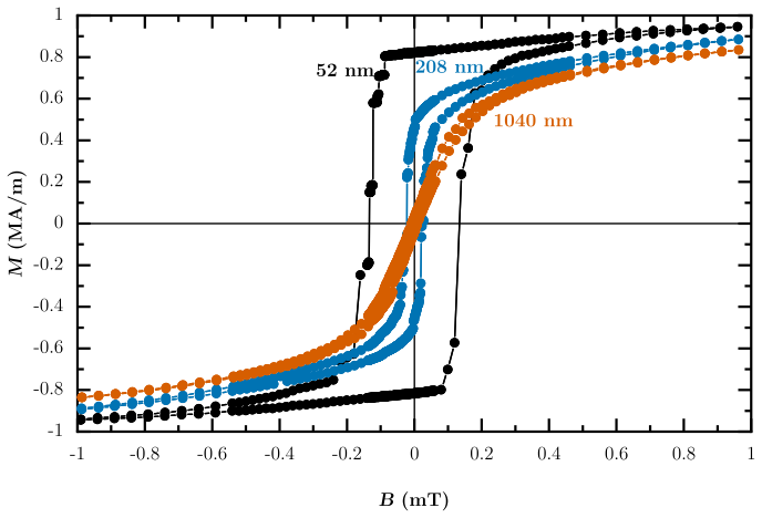
The central discovery claimed by the paper is that for RF-sputtered amorphous Co91Nb7Zr2 films, film thickness is the controlling parameter for soft magnetic properties, independent of composition or crystallinity. The paper reports that saturation magnetization remains constant at (1.01 ± 0.04) MA/m from 52 nm to 1040 nm, while coercivity falls by a factor of ten to about 10 A/m, the remanent-to-saturation ratio falls by a factor of sixteen to 0.05, and the maximum permeability number falls by a factor of five to 4×$10^{4}$. The same thickness sweep changes the remanent domain state from irregular cross-tie walls in the 52 nm film to a regular flux-closure diamond state at 208 nm. The authors interpret this as the signature of a transition from Néel-type to Bloch-type domain walls, which they estimate, using D = 20√(A/K_d) with the literature exchange constant A = 11 pJ/m and their measured magnetization, to occur at roughly 84 nm. They further explain the thickness-dependent coercivity and remanence through demagnetization fields that grow from about 0.04 mT to 0.51 mT and through surface anisotropy that weakens as the film thickens.
Load-bearing premise
The explanation of the domain images as a Néel-to-Bloch wall transition depends on the literature exchange constant A = 11 pJ/m being accurate for this specific Co91Nb7Zr2 composition; if the true exchange constant differs, the predicted 84 nm crossover shifts and the claimed structural origin of the magnetic trends loses its anchor.
Editorial extensions
If this is right
- Film thickness alone can be used to engineer softness in amorphous CoNbZr: a roughly 1 µm film reaches a coercivity of about 10 A/m and a maximum permeability number of 4×10^4.
- Since saturation magnetization does not change with thickness, making the film thicker to gain softness does not sacrifice magnetic moment per volume.
- Below the predicted crossover near 84 nm, remanent domains should be Néel-type with cross-ties; above it, Bloch-type flux-closure states should dominate, matching the two imaged thicknesses.
- The demagnetization field rising from about 0.04 mT to 0.51 mT means thicker films need stronger applied fields to saturate, which explains the transition from square to smooth loops.
- Multilayer CoNbZr stacks with optimized interlayer thickness should give a higher giant magnetoimpedance ratio and sensitivity than a single 1 µm film of the same total magnetic thickness.
Reading between the lines
- A sharper test of the wall-transition explanation, which the paper does not perform, is to image films at intermediate thicknesses around 84 nm, 104 nm, and 120 nm; if cross-tie walls persist far above the predicted crossover, the assumed exchange constant is off for this alloy.
- The same mechanism implies that varying the Nb/Zr content, which changes the exchange constant, should shift the crossover thickness; determining A for Co91Nb7Zr2 directly would turn the 84 nm estimate into a tested prediction.
- The very low remanence ratio at 1040 nm suggests films of that thickness are almost fully flux-closed at remanence, which could make them less responsive to small applied fields in sensor geometries despite their lower coercivity; the paper does not discuss this trade-off.
- Because surface anisotropy is invoked to explain the higher coercivity of thin films, modifying the film surfaces or interfaces should change Hc most strongly in the thinnest samples; this is a testable consequence of the paper's mechanism.
Editorial analysis
A structured set of objections, weighed in public.
Referee Report
Summary. The paper reports a systematic thickness series (52–1040 nm) of RF-sputtered amorphous Co91Nb7Zr2 films. Structural characterisation by XRD, electron diffraction, and EDX indicates an amorphous structure with composition Co91±1Nb7±1Zr2±1. VSM measurements show a thickness-independent saturation magnetisation of (1.01±0.04) MA/m, while coercivity, remanence ratio, and maximum permeability decrease with increasing thickness. MFM on 20 µm patterned squares at 52 nm and 208 nm shows irregular cross-tie domains versus flux-closure domains, and the authors attribute the change to a Néel-to-Bloch wall transition expected at approximately 84 nm, estimated using a literature exchange constant and the measured saturation magnetisation. The conclusion suggests implications for multilayer GMI sensors.
Significance. If the empirical trends hold, the dataset is a useful contribution to the soft-magnetic thin-film literature, especially because Ms is cross-checked by two independent methods and the film series is systematic. A notable strength is that the only fitted parameter in the analysis is the linear diamagnetic background slope; the remaining quantities are measured directly or taken from literature. However, the central mechanistic claim, the 84 nm Néel–Bloch crossover, is only weakly supported by two MFM images and an external exchange constant, and the maximum-permeability extraction is not documented. The paper is therefore a plausible empirical study whose interpretive conclusion needs substantial strengthening.
major comments (4)
- [Abstract, §3.2, Fig. 7] The abstract states that films above 208 nm exhibit flux-closure domain structures, but MFM was performed only at 52 nm and 208 nm. The flux-closure observation is therefore limited to a single thickness; no data support the behaviour at 520 or 1040 nm. Please restrict the domain-structure claim to the measured thicknesses or add MFM data at intermediate or larger thicknesses.
- [§3.2, §3.3] The 84 nm Néel–Bloch transition is an interpolation between two widely spaced MFM thicknesses, not a fitted or measured crossover. The estimate uses D=20√(A/Kd) with A=11 pJ/m from Ref. [34] and Kd derived from Ms only, but §3.3 invokes a thickness-dependent perpendicular surface anisotropy at 52 nm, which is not included in the estimate. Because the true crossover could lie outside the 52–208 nm interval, the two MFM images do not discriminate between the proposed mechanism and alternatives. Please provide a sensitivity analysis of the crossover to A and to a plausible perpendicular anisotropy, or reframe the wall-transition explanation as tentative.
- [§2.3, Fig. 6(c)] The maximum permeability number µmax is one of the three central thickness-dependent quantities, but the manuscript nowhere defines how it was obtained. It is not stated whether µmax is computed from the slope of the VSM loops (and over which field range) or measured by a separate permeability method, and no uncertainties are given for µmax. Please add the extraction procedure, the defining equation, and error estimates.
- [§3.2 vs. §3.3] The paper offers two overlapping explanations for the thickness trends: the Néel–Bloch wall transition in §3.2, and the demagnetising-field/surface-anisotropy arguments in §3.3. These are not reconciled; in particular, the coercivity decrease is attributed to reduced surface anisotropy in §3.3 but to the wall-type change in §3.2. The manuscript should state which mechanism is primary or explain how the two are connected.
minor comments (6)
- [§2.2] The goniometer radius is given as 280 nm; this is presumably 280 mm. Please correct.
- [§3.1] The sentence 'A notable observation in Figs. 6(a) and 6(b) is that the uncertainty in the measure fields decrease with increasing thickness' contains a grammatical error ('measure fields' should be 'measured fields') and a subject-verb disagreement.
- [§3.2] When introducing Kd in the expression D=20√(A/Kd), please define Kd (e.g., Kd = μ0Ms²/2 for a thin film with no perpendicular anisotropy) and give the source or derivation of the numerical prefactor 20.
- [Table 3] The definition of p_Co in the formula n_B = p_CoMs/(μB NCo) is not given; please define the Co concentration variable and state its numerical value for Co91Nb7Zr2.
- [Fig. 7] The MFM images are taken on 20 µm×20 µm patterned elements, whereas the Néel–Bloch transition estimate applies to an extended film; please comment on whether lateral confinement could affect the observed wall type.
- [§2.1, §3.1] The target composition Co85Nb12Zr3 was chosen for near-zero magnetostriction, but the deposited films are Co91Nb7Zr2; please address whether the magnetostriction of the actual film composition was considered.
Circularity Check
No circularity: the 84 nm Néel–Bloch crossover is an external-formula prediction from measured Ms and a literature exchange constant, not fitted to the MFM images.
full rationale
The paper's central claims are extracted directly from VSM hysteresis loops: Ms, Hc, Mr/Ms, and μmax are measured quantities, and their thickness dependence is presented as data, not derived from a fitted model. The only fitted parameter is the small diamagnetic background correction of 0.5 μAm²/T, which does not enter the central results. The Néel–Bloch wall transition at approximately 84 nm is computed from the formula D = 20√(A/Kd), using a literature exchange constant A = 11 pJ/m from Ref. [34] and Kd derived from the independently measured saturation magnetization; it is not fitted to the MFM images. The MFM images at 52 nm and 208 nm are then compared qualitatively as a consistency check, not used as inputs to the calculation. There are no load-bearing self-citations: the reference list contains no works by the present authors. Concerns about the accuracy of the literature value A or the sparse thickness sampling of the MFM data are evidence-weighting issues, not circularity. The derivation chain is therefore self-contained relative to its stated inputs.
Assumptions & free parameters
free parameters (1)
- diamagnetic background slope =
0.5 µAm^2/T
assumptions (6)
- domain assumption The CoNbZr films remain amorphous and compositionally homogeneous across the entire thickness range.
- domain assumption MFM images of patterned 20 µm by 20 µm squares are representative of the unpatterned continuous films measured by VSM.
- domain assumption The literature exchange constant A=11 pJ/m (Ref. [34]) applies to the Co91Nb7Zr2 composition.
- domain assumption The diamagnetic background is a linear function of field with slope 0.5 µAm^2/T.
- domain assumption The quoted Néel-Bloch transition criterion D=20*sqrt(A/Kd) from Ref. [33] is valid for these film geometries.
- standard math Demagnetization factors Nx computed from Aharoni's formulas correctly describe the 8 mm by 8 mm film geometry.
Cite this review
Pith. "Pith review of Influence of thickness on magnetic properties of RF-sputtered amorphous CoNbZr thin films." pith.science (2026). https://pith.science/paper/MKLDF74M
@misc{pith2026250522077,
  author       = {Pith},
  title        = {Pith review of: Influence of thickness on magnetic properties of RF-sputtered amorphous CoNbZr thin films},
  year         = {2026},
  howpublished = {\url{https://pith.science/paper/MKLDF74M}},
  note         = {Machine review of arXiv:2505.22077}
}
abstract
Amorphous sputtered Co-based thin films are widely used as soft magnetic materials in applications such as sensors, inductors and magnetic flux concentrators. The magnetic properties of these films can be controlled by deposition parameters like film thickness, argon pressure, deposition rate and others. In this study, we present a detailed investigation of the magnetic properties of RF-sputtered Co$_{91}$Nb$_7$Zr$_2$ films with thicknesses ranging from 52 nm to 1040 nm. These amorphous films exhibit an average saturation magnetisation of 1.01(4) MA/m. As the film thickness increases, there is a significant decrease in coercivity, remanent-to-saturation magnetisation ratio M$_r$/M$_s$, and maximum permeability. The change in macroscopic magnetic properties is also reflected by the domain structure. At a thickness of 52 nm, the remanent domain state shows irregular domains, while films thicknesses above 208 nm exhibit flux-closure domain structures instead. The thickness-dependent modifications are attributed to the transition between N\'eel and Bloch type domain walls, which is expected to occur at approximately 84 nm.
Figures


Figures from the paper (4 more)



Reference graph
Works this paper leans on
-
[34]
A. Yoshihara, K. Takanashi, M. Shimoda, O. Kitakami, and Y. Shimada, Japanese Journal of Applied Physics33, 3927 (1994)
work page 1994
- [1]
-
[2]
Sakakima, IEEE Transactions on Magnetics19, 131 (1983)
H. Sakakima, IEEE Transactions on Magnetics19, 131 (1983)
work page 1983
- [3]
-
[4]
Meydan, Journal of Magnetism and Magnetic Materials133, 525 (1994)
T. Meydan, Journal of Magnetism and Magnetic Materials133, 525 (1994)
work page 1994
-
[5]
C. P. O. Treutler, Sensors and Actuators, A: Physical91, 2 (2001)
work page 2001
- [6]
-
[7]
Korenivski, Journal of Magnetism and Magnetic Materials215, 800 (2000)
V. Korenivski, Journal of Magnetism and Magnetic Materials215, 800 (2000)
work page 2000
Show all 35 references
-
[8]
M. S. Ryłko, K. J. Hartnett, J. G. Hayes, and M. G. Egan, Conference Proceedings - IEEE Applied Power Electronics Conference and Exposition - APEC , 2043 (2009)
2009
-
[9]
H. I. Hsiang, L. C. Wu, C. C. Chen, and W. H. Lee, Materials15, 1 (2022)
2022
-
[10]
Hasegawa, Materials Science and Engineering: A375-377, 90 (2004)
R. Hasegawa, Materials Science and Engineering: A375-377, 90 (2004)
2004
-
[11]
F. Chai, Z. Li, L. Chen, and Y. Pei, IEEE Transactions on Magnetics57, 1 (2020). 17
2020
-
[12]
Enomoto, R
Y. Enomoto, R. Takahata, D. Satoh, Y. Marukawa, and H. Sano, IEEJ Journal of Industry Applications12, 1127 (2023)
2023
-
[13]
H. J. de Wit, C. H. M. Witmer, and F. W. A. Dirne, IEEE Transactions on Magnetics23, 2123 (1987)
1987
-
[14]
Żuberek, H
R. Żuberek, H. Szymczak, D. Żymierska, G. Suran, and M. Naili, Journal of Magnetism and Magnetic Materials104-107, 117 (1992)
1992
-
[15]
Marinho, S
Z. Marinho, S. Cardoso, R. Chaves, R. Ferreira, L. V. Melo, and P. P. Freitas, Journal of Applied Physics109, 07E521 (2011)
2011
-
[16]
G. He, Y. Zhang, L. Qian, G. Xiao, Q. Zhang, J. C. Santamarina, T. W. Patzek, and X. Zhang, Applied Physics Letters113, 242401 (2018)
2018
-
[17]
Maspero, S
F. Maspero, S. Cuccurullo, D. Mungpara, A. Schwarz, and R. Bertacco, Journal of Magnetism and Magnetic Materials535, 168072 (2021)
2021
-
[18]
B. Peng, W. L. Zhang, Q. Y. Xie, W. X. Zhang, and H. C. Jiang, Journal of Non-Crystalline Solids365, 59 (2013)
2013
-
[19]
Takahashi, M
T. Takahashi, M. Yoneda, and M. Naoe, Japanese Journal of Applied Phys- ics28, 379 (1989)
1989
-
[20]
X. W. Li, C. Song, J. Yang, F. Zeng, K. W. Geng, and F. Pan, Journal of Magnetism and Magnetic Materials315, 120 (2007)
2007
-
[21]
Cao and C
Y. Cao and C. Zhou, Journal of Magnetism and Magnetic Materials324, 1832 (2012)
2012
-
[22]
Katada, T
H. Katada, T. Shimatsu, I. Watanabe, H. Muraoka, Y. Nakamura, and Y. Sugita, Journal of the Magnetics Society of Japan24, 539 (2000)
2000
-
[23]
Yamaguchi, S
M. Yamaguchi, S. Tanaka, Y. Endo, S. Muroga, and M. Nagata, 2015 Asia-Pacific International Symposium on Electromagnetic Compatibility (APEMC) , 536 (2015). 18
2015
-
[24]
Fassbender and J
J. Fassbender and J. McCord, Journal of Magnetism and Magnetic Mater- ials320, 579 (2008)
2008
-
[25]
Tomus and H
D. Tomus and H. P. Ng, Micron44, 115 (2013)
2013
-
[26]
Crangle and G
J. Crangle and G. M. Goodman, Proceedings of the Royal Society of Lon- don. A. Mathematical and Physical Sciences321, 477 (1971)
1971
-
[27]
Babcock, V
K. Babcock, V. Elings, M. Dugas, and S. Loper, IEEE Transactions on Magnetics30, 4503 (1994)
1994
-
[28]
Cullity and S
B. Cullity and S. Stock,Elements of X-Ray Diffraction: Third Edition (Pearson Education Limited, 2014)
2014
-
[29]
Neidhardt, S
J. Neidhardt, S. Mráz, J. M. Schneider, E. Strub, W. Bohne, B. Liedke, W. Möller, and C. Mitterer, Journal of Applied Physics104, 10.1063/1.2978211 (2008)
2008 doi
-
[30]
L. Sun, Y. Hao, C. L. Chien, P. C. Searson, and P. C. Searson, IBM Journal of Research and Development49, 79 (2005)
2005
-
[31]
Ohnuma, K
S. Ohnuma, K. Shirakawa, M. Nose, and T. Masumoto, IEEE Transactions on Magnetics16, 1129 (1980)
1980
-
[32]
Lekdadri, R
A. Lekdadri, R. Chami, A. Saadi, H. Lassri, and L. H. Omari, Materials Today: Proceedings37, 3813 (2020)
2020
-
[33]
Hubert and R
A. Hubert and R. Schäfer,Magnetic Domains(Springer Berlin Heidelberg, 2009)
2009
-
[35]
Aharoni, Journal of Applied Physics83, 3432 (1998)
A. Aharoni, Journal of Applied Physics83, 3432 (1998). 19
1998
Reviewed August 7, 2026 · model on record in the stance chip above.
Discussion (0). Sign in to comment.