How nanotextured interfaces influence the electronics in perovskite solar cells
Pith reviewed 2026-05-19 10:02 UTC · model grok-4.3
The pith
Nanotexturing redistributes the electric field in perovskite solar cells and raises power conversion efficiency for heights up to 300 nm.
A machine-rendered reading of the paper's core claim, the machinery that carries it, and where it could break.
Core claim
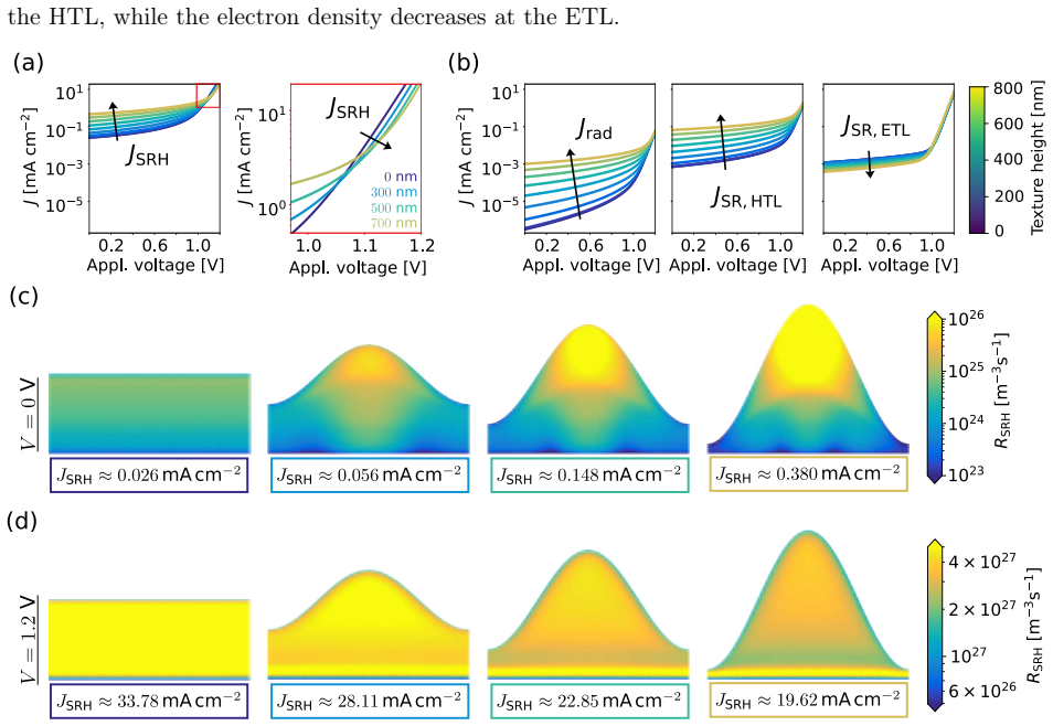
Texturing redistributes the electric field, influencing carrier accumulation and recombination dynamics. Moderate texturing heights (≤ 300 nm) always increase the power conversion efficiency, regardless of surface recombination velocities. This behaviour originates from variations in surface recombination at the untextured electron transport layer, which controls open-circuit voltage, while recombination at the textured hole transport layer controls short-circuit current density.
What carries the argument
Multi-dimensional optical and charge-transport simulations that solve light propagation together with electrostatic potential and carrier continuity equations across the textured geometry.
If this is right
- Moderate nanotexturing improves efficiency even when surface recombination is high.
- Open-circuit voltage changes in experiments trace to recombination differences at the flat electron transport layer.
- Short-circuit current stays closer to the optical limit when recombination at the textured hole transport layer is low.
- The same texture design principles apply to perovskite light-emitting diodes and photodetectors.
Where Pith is reading between the lines
- Texture height could be chosen mainly for optics while surface passivation is tuned separately for electronics.
- Similar field-redistribution effects may appear in other thin-film solar cells that use nano-textured contacts.
- Long-term stability might improve if the redistributed field reduces local carrier densities that drive degradation.
Load-bearing premise
The chosen simulation geometry and material parameters correctly reproduce the real electric-field patterns and interface recombination rates that occur in fabricated devices.
What would settle it
Fabricate single-junction perovskite cells with controlled 300 nm interface textures and flat controls, measure power conversion efficiency while varying only the electron-transport-layer surface recombination velocity, and check whether efficiency rises in every case.
Figures


read the original abstract
Perovskite solar cells have reached power conversion efficiencies that rival those of established silicon photovoltaics. Nanotextures in perovskite solar cells scatter the incident light, thereby improving optical absorption. In addition, experiments show that nanotextures impact electronic performance, although the underlying mechanisms remain unclear. This study investigates the underlying theoretical reasons by combining multi-dimensional optical and charge-transport simulations for a single-junction perovskite solar cell. Our numerical results reveal that texturing redistributes the electric field, influencing carrier accumulation and recombination dynamics. We find that moderate texturing heights ($\leq 300$ nm) always increase the power conversion efficiency, regardless of surface recombination velocities. Our study also clarifies why experiments have reported that texturing both increased and reduced open-circuit voltages in perovskite solar cells: this behaviour originates from variations in surface recombination at the untextured electron transport layer. In contrast, surface recombination at the textured hole transport layer strongly affects the short-circuit current density, with lower recombination rates keeping it closer to the optical ideal. These findings provide new insights into the opto-electronic advantages of texturing and offer guidance for the design of next-generation textured perovskite-based solar cells, light emitting diodes, and photodetectors.
Editorial analysis
A structured set of objections, weighed in public.
Referee Report
Summary. The manuscript uses multi-dimensional optical and charge-transport simulations of a single-junction perovskite solar cell to investigate the electronic effects of nanotextured interfaces. It claims that texturing redistributes the internal electric field, thereby altering carrier accumulation and recombination dynamics. Moderate texturing heights (≤ 300 nm) are reported to increase power conversion efficiency for all tested surface recombination velocities. The work further explains conflicting experimental reports on open-circuit voltage by attributing them to surface recombination at the untextured electron transport layer, while recombination at the textured hole transport layer primarily influences short-circuit current density.
Significance. If the numerical trends hold, the paper makes a useful contribution by clarifying the opto-electronic mechanisms of nanotexturing in perovskite devices beyond simple light scattering. The results are generated from standard first-principles transport equations solved on the textured geometry without fitted parameters introduced to force efficiency gains, and consistent trends are shown across multiple recombination velocities and texture heights. This provides mechanistic insight into experimental observations and practical guidance for interface design in solar cells, LEDs, and photodetectors.
major comments (1)
- Simulation setup and boundary conditions: No mesh-convergence study or grid-independence test is reported. Because the central claims concerning electric-field redistribution, carrier profiles, and efficiency gains rest on numerical solutions of the drift-diffusion equations in complex nanotextured geometries, explicit verification that the quantitative trends are insensitive to mesh refinement is needed to establish robustness.
minor comments (2)
- Abstract: The unqualified statement that moderate texturing 'always' increases efficiency should be limited to the simulated range of parameters and geometries to prevent overgeneralization.
- Results figures: Direct side-by-side comparison of electric-field and carrier-density maps for textured versus planar reference cases would improve clarity and allow readers to assess the magnitude of the redistribution effect.
Simulated Author's Rebuttal
We thank the referee for the positive evaluation of our work and for the constructive comment on numerical robustness. We address the point below and will revise the manuscript accordingly to strengthen the presentation of our simulation results.
read point-by-point responses
-
Referee: Simulation setup and boundary conditions: No mesh-convergence study or grid-independence test is reported. Because the central claims concerning electric-field redistribution, carrier profiles, and efficiency gains rest on numerical solutions of the drift-diffusion equations in complex nanotextured geometries, explicit verification that the quantitative trends are insensitive to mesh refinement is needed to establish robustness.
Authors: We agree that explicit demonstration of mesh independence is essential for establishing the robustness of results obtained from drift-diffusion simulations on complex geometries. Although our simulations employed adaptive mesh refinement with a minimum element size chosen to resolve the nanotextured interfaces and boundary layers (typically <10 nm near surfaces), we did not include a dedicated convergence study in the original manuscript. In the revised version we will add a new subsection (or supplementary note) that reports the results of systematic mesh refinement: we will show that the electric-field profiles, carrier densities, recombination rates, and power-conversion efficiency change by less than 1 % when the mesh is further refined by a factor of two, confirming that the reported trends are insensitive to discretization. revision: yes
Circularity Check
No significant circularity detected
full rationale
The paper derives its central claims by numerically solving coupled optical and drift-diffusion transport equations on explicitly defined nanotextured geometries with stated boundary conditions and material parameters. The reported field redistribution, carrier accumulation changes, and PCE increase for texturing heights ≤300 nm emerge directly from these first-principles PDE solutions without any fitted parameters, self-definitional loops, or load-bearing self-citations that reduce the output to the input. No ansatz is smuggled via prior work, no uniqueness theorem is invoked to force choices, and no known empirical pattern is merely renamed. The derivation chain is therefore self-contained and independent of the target results.
Axiom & Free-Parameter Ledger
free parameters (2)
- texture height
- surface recombination velocities
axioms (2)
- domain assumption Drift-diffusion equations with standard boundary conditions accurately describe carrier transport in the perovskite and transport layers.
- domain assumption Maxwell equations with appropriate scattering boundary conditions capture the optical field redistribution caused by the nanotexture.
Lean theorems connected to this paper
-
IndisputableMonolith/Cost/FunctionalEquationwashburn_uniqueness_aczel unclear?
unclearRelation between the paper passage and the cited Recognition theorem.
We employ a vacancy-assisted drift-diffusion model ... solving the drift-diffusion equations ... Shockley-Read-Hall (SRH) recombination ...
-
IndisputableMonolith/Foundation/RealityFromDistinctionreality_from_one_distinction unclear?
unclearRelation between the paper passage and the cited Recognition theorem.
multi-dimensional optical and charge-transport simulations ... finite element (FE) mesh ... finite volume (FV) mesh
What do these tags mean?
- matches
- The paper's claim is directly supported by a theorem in the formal canon.
- supports
- The theorem supports part of the paper's argument, but the paper may add assumptions or extra steps.
- extends
- The paper goes beyond the formal theorem; the theorem is a base layer rather than the whole result.
- uses
- The paper appears to rely on the theorem as machinery.
- contradicts
- The paper's claim conflicts with a theorem or certificate in the canon.
- unclear
- Pith found a possible connection, but the passage is too broad, indirect, or ambiguous to say the theorem truly supports the claim.
Reference graph
Works this paper leans on
-
[1]
Next- generation applications for integrated perovskite solar cells
A. S. R. Bati, Y. L. Zhong, P. L. Burn, M. K. Nazeeruddin, P. E. Shaw, and M. Batmunkh. “Next- generation applications for integrated perovskite solar cells”. In: Communications Materials 4.1 (2023), p. 2
work page 2023
-
[2]
Optics for terawatt-scale photovoltaics: review and perspectives
K. Jäger et al. “Optics for terawatt-scale photovoltaics: review and perspectives”. In: Adv. Opt. Photonics 17.1 (Feb. 2025), pp. 185–294
work page 2025
-
[3]
Homogenized contact in all-perovskite tandems using tailored 2D perovskite
Y. Wang et al. “Homogenized contact in all-perovskite tandems using tailored 2D perovskite”. In: Nature 635 (2024), pp. 867–873
work page 2024
-
[4]
Perovskite/silicon tandem solar cells with bilayer interface passivation
J. Liu et al. “Perovskite/silicon tandem solar cells with bilayer interface passivation”. In: Nature 635 (2024), pp. 596–603. 16
work page 2024
-
[5]
Z. Liu et al. “All-perovskite tandem solar cells achieving> 29% efficiency with improved (100) orientation in wide-bandgap perovskites”. In: Nature Materials 24 (2025), pp. 252–259
work page 2025
-
[6]
Highly Efficient Monolithic Perovskite/TOPCon Silicon Tandem Solar Cells Enabled by “Halide Locking
L. Wang et al. “Highly Efficient Monolithic Perovskite/TOPCon Silicon Tandem Solar Cells Enabled by “Halide Locking””. In: Advanced Materials 37.7 (2025), p. 2416150
work page 2025
-
[7]
Enhanced cation interaction in perovskites for efficient tandem solar cells with silicon
E. Ugur, A. A. Said, P. Dally, S. Zhang, C. E. Petoukhoff, D. Rosas-Villalva, S. Zhumagali, B. K. Yildirim, A. Razzaq, S. Sarwade, et al. “Enhanced cation interaction in perovskites for efficient tandem solar cells with silicon”. In: Science 385.6708 (2024), pp. 533–538
work page 2024
-
[8]
P. Tockhorn et al. “Improved quantum efficiency by advanced light management in nanotextured solution-processed perovskite solar cells”. In: ACS Photonics 7.9 (2020), pp. 2589–2600
work page 2020
-
[9]
Fully textured monolithic perovskite/silicon tandem solar cells with 25.2% power conversion efficiency
F. Sahli et al. “Fully textured monolithic perovskite/silicon tandem solar cells with 25.2% power conversion efficiency”. In: Nature Materials 17.9 (2018). Publisher: Springer US, pp. 820–826
work page 2018
-
[10]
B. Chen et al. “Blade-Coated Perovskites on Textured Silicon for 26%-Efficient Monolithic Perovskite/Silicon Tandem Solar Cells”. In: Joule 4.4 (Apr. 2020), pp. 850–864
work page 2020
-
[11]
Efficient tandem solar cells with solution-processed perovskite on textured crystalline silicon
Y. Hou et al. “Efficient tandem solar cells with solution-processed perovskite on textured crystalline silicon”. eng. In: Science 367.6482 (Mar. 2020), pp. 1135–1140
work page 2020
-
[12]
Efficient and stable perovskite-silicon tandem solar cells through contact displacement by MgF x
J. Liu, M. De Bastiani, E. Aydin, G. T. Harrison, Y. Gao, R. R. Pradhan, M. K. Eswaran, M. Mandal, W. Yan, A. Seitkhan, et al. “Efficient and stable perovskite-silicon tandem solar cells through contact displacement by MgF x”. In: Science 377.6603 (2022), pp. 302–306
work page 2022
-
[13]
Nano-optical designs for high-efficiency monolithic perovskite–silicon tandem solar cells
P. Tockhorn et al. “Nano-optical designs for high-efficiency monolithic perovskite–silicon tandem solar cells”. In: Nature Nanotechnology 17.11 (2022), pp. 1214–1221
work page 2022
-
[14]
J. Zheng, H. Wei, Z. Ying, X. Yang, J. Sheng, Z. Yang, Y. Zeng, and J. Ye. “Balancing charge-carrier transport and recombination for perovskite/TOPCon tandem solar cells with double-textured structures”. In: Advanced Energy Materials 13.5 (2023), p. 2203006
work page 2023
-
[15]
O. Er-Raji, C. Messmer, A. J. Bett, O. Fischer, S. K. Reichmuth, F. Schindler, M. Bivour, O. Schultz-Wittmann, J. Borchert, M. Hermle, et al. “Loss Analysis of Fully-Textured Perovskite Silicon Tandem Solar Cells: Characterization Methods and Simulation toward the Practical Efficiency Potential”. In: Solar RRL 7.24 (2023), p. 2300659
work page 2023
-
[16]
M. T. Neukom et al. “Consistent Device Simulation Model Describing Perovskite Solar Cells in Steady-State, Transient, and Frequency Domain”. In: ACS Applied Materials & Interfaces 11.26 (2019), pp. 23320–23328
work page 2019
-
[17]
U. Aeberhard, S. Zeder, and B. Ruhstaller. “Effects of Photon Recycling and Luminescent Coupling in All-Perovskite Tandem Solar Cells Assessed by Full Opto-electronic Simulation”. In: Solar RRL 8 (June 2024)
work page 2024
-
[18]
C. Messmer, D. Chojniak, A. J. Bett, S. K. Reichmuth, J. Hohl-Ebinger, M. Bivour, M. Hermle, J. Schön, M. C. Schubert, and S. W. Glunz. “Toward more reliable measurement procedures of perovskite-silicon tandem solar cells: The role of transient device effects and measurement conditions”. In: Progress in Photovoltaics: Research and Applications 33.1 (2025),...
work page 2025
-
[19]
W. Clarke, L. Bennett, Y. Grudeva, J. Foster, G. Richardson, and N. Courtier. “IonMonger 2.0: software for free, fast and versatile simulation of current, voltage and impedance response of planar perovskite solar cells”. In: Journal of Computational Electronics 22 (2022), pp. 364–382. 17
work page 2022
-
[20]
P. Calado, I. Gelmetti, B. Hilton, M. Azzouzi, J. Nelson, and P. R. F. Barnes. “Driftfusion: An open source code for simulating ordered semiconductor devices with mixed ionic-electronic conducting materials in one-dimension”. In: Journal of Computational Electronics 21 (2022), pp. 960–991
work page 2022
-
[21]
SIMsalabim: An open-source drift-diffusion simulator for semiconductor devices
M. Koopmans, V. M. Le Corre, and L. J. A. Koster. “SIMsalabim: An open-source drift-diffusion simulator for semiconductor devices”. In: Journal of Open Source Software 7.70 (2022), p. 3727
work page 2022
-
[22]
Pathways toward 30% efficient single-junction perovskite solar cells and the role of mobile ions
J. Diekmann, P. Caprioglio, M. H. Futscher, V. M. Le Corre, S. Reichert, F. Jaiser, M. Arvind, L. P. Toro, E. Gutierrez-Partida, F. Pena-Camargo, et al. “Pathways toward 30% efficient single-junction perovskite solar cells and the role of mobile ions”. In: Solar RRL 5.8 (2021), p. 2100219
work page 2021
-
[23]
C.-H. Hsieh, J. -Y. Huang, and Y. -R. Wu. “Analysis of two-terminal perovskite/silicon tandem solar cells with differing texture structure, perovskite carrier lifetime, and tunneling junction quality”. In: Journal of Applied Physics 135.11 (2024), p. 115002
work page 2024
-
[24]
Optimization of MAPbI 3-Based Perovskite Solar Cell With Textured Surface
J.-Y. Huang, E. -W. Chang, and Y. -R. Wu. “Optimization of MAPbI 3-Based Perovskite Solar Cell With Textured Surface”. In: IEEE Journal of Photovoltaics 9.6 (2019), pp. 1686–1692
work page 2019
-
[25]
V. M. Le Corre et al. “Quantification of Efficiency Losses Due to Mobile Ions in Perovskite Solar Cells via Fast Hysteresis Measurements”. In: Solar RRL 6.4 (2022), p. 2100772
work page 2022
-
[26]
Advanced Light Management Concepts for Silicon and Perovskite Based Solar Cells
J. Sutter. “Advanced Light Management Concepts for Silicon and Perovskite Based Solar Cells”. PhD thesis. Technische Universiät Berlin, 2022
work page 2022
-
[27]
Adaptive finite element method for simulation of optical nano structures
J. Pomplun, S. Burger, L. Zschiedrich, and F. Schmidt. “Adaptive finite element method for simulation of optical nano structures”. In: Phys. Stat. Sol. B 244 (2007), p. 3419
work page 2007
-
[28]
Department of Energy (DOE)/NREL/ALLIANCE
U.S. Department of Energy (DOE)/NREL/ALLIANCE. Reference Air Mass 1.5 Spectra . https://www.nrel.gov/grid/solar-resource/spectra-am1.5.html
-
[29]
Nanophotonic light management for perovskite–silicon tandem solar cells
D. Chen, P. Manley, P. Tockhorn, D. Eisenhauer, G. Köppel, M. Hammerschmidt, S. Burger, S. Albrecht, C. Becker, and K. Jäger. “Nanophotonic light management for perovskite–silicon tandem solar cells”. In: Journal of Photonics for Energy 8.2 (2018), p. 022601
work page 2018
-
[30]
Y. Yuan, G. Yan, S. Akel, U. Rau, and T. Kirchartz. “Deriving mobility-lifetime products in halide perovskite films from spectrally and time-resolved photoluminescence”. In: Science Advances 11.16 (2025), eadt1171
work page 2025
-
[31]
P. Würfel and U. Würfel. Physics of Solar Cells: From Basic Principles to Advanced Concepts . 3rd ed. Wiley-VCH Verlag GmbH & Co, Weinheim, 2016
work page 2016
-
[32]
Dielectric Junction: Electrostatic Design for Charge Carrier Collection in Solar Cells
J. Hüpkes, U. Rau, and T. Kirchartz. “Dielectric Junction: Electrostatic Design for Charge Carrier Collection in Solar Cells”. In: Solar RRL 6.1 (2022), p. 2100720
work page 2022
-
[33]
M. Stolterfoht et al. “The impact of energy alignment and interfacial recombination on the internal and external open-circuit voltage of perovskite solar cells”. In: Energy Environ. Sci. 12 (2019), pp. 2778–2788
work page 2019
-
[34]
P. Caprioglio, M. Stolterfoht, C. M. Wolff, T. Unold, B. Rech, S. Albrecht, and D. Neher. “On the relation between the open-circuit voltage and quasi-fermi level splitting in efficient perovskite solar cells”. In: Advanced Energy Materials 9.33 (2019), p. 1901631. 18
work page 2019
-
[35]
Modelling charge transport in perovskite solar cells: Potential-based and limiting ion depletion
D. Abdel, P. Vágner, J. Fuhrmann, and P. Farrell. “Modelling charge transport in perovskite solar cells: Potential-based and limiting ion depletion”. In: Electrochimica Acta 390 (2021), p. 138696
work page 2021
-
[36]
Modeling and simulation of vacancy-assisted charge transport in innovative semi- conductor devices
D. Abdel. “Modeling and simulation of vacancy-assisted charge transport in innovative semi- conductor devices”. PhD Thesis. Freie Universität Berlin, 2024
work page 2024
-
[37]
P. Farrell, D. H. Doan, M. Kantner, J. Fuhrmann, T. Koprucki, and N. Rotundo. “Drift-Diffusion Models”. In: Handbook of Optoelectronic Device Modeling and Simulation: Lasers, Modulators, Photodetectors, Solar Cells, and Numerical Methods, Vol. 2 . CRC Press Taylor & Francis Group, 2017, pp. 733–771
work page 2017
-
[38]
Numerical analysis of a finite volume scheme for charge transport in perovskite solar cells
D. Abdel, C. Chainais-Hillairet, P. Farrell, and M. Herda. “Numerical analysis of a finite volume scheme for charge transport in perovskite solar cells”. In: IMA Journal of Numerical Analysis 44 (2024), p. 1090
work page 2024
-
[39]
D. Abdel, P. Farrell, and J. Fuhrmann. “Assessing the quality of the excess chemical potential flux scheme for degenerate semiconductor device simulation”. In: Optical and Quantum Electronics 53.163 (2021), p. 163
work page 2021
- [40]
-
[41]
J. Fuhrmann, P. Jaap, D. Runge, D. Abdel, J. Weidner, A. Seiler, P. Farrell, and M. Liero. VoronoiFVM.jl - Finite volume solver for coupled nonlinear partial differential equations
-
[42]
Algorithm 832: UMFPACK V4.3—an unsymmetric-pattern multifrontal method
T. A. Davis. “Algorithm 832: UMFPACK V4.3—an unsymmetric-pattern multifrontal method”. In: ACM Trans. Math. Softw. 30.2 (June 2004), pp. 196–199
work page 2004
-
[43]
Triangle: Engineering a 2D quality mesh generator and Delaunay triangulator
J. R. Shewchuk. “Triangle: Engineering a 2D quality mesh generator and Delaunay triangulator”. In: Applied Computational Geometry Towards Geometric Engineering . Ed. by M. C. Lin and D. Manocha. Springer-Verlag, Berlin Heidelberg, 1996, pp. 203–222
work page 1996
-
[44]
M. Kittisopikul, T. E. Holy, and T. Aschan. Interpolations.jl. Version 0.16.0. May 2025
work page 2025
-
[45]
D. Abdel, J. Relle, T. Kirchartz, P. Jaap, J. Fuhrmann, S. Burger, C. Becker, K. Jäger, and P. Farrell. TexturedPerovskiteSolarCells.jl – Numerical examples to analyse the electronic behaviour of textured perovskite solar cells . Version 1.0.0. 19 Electronic Supplementary Information Unravelling the mystery of enhanced open-circuit voltages in nanotexture...
work page 2012
discussion (0)
Sign in with ORCID, Apple, or X to comment. Anyone can read and Pith papers without signing in.