REVIEW 4 major objections 6 minor 52 references
Compact detector for atom-atom correlations on an atom chip
T0 review · 4 major / 6 minor · reviewed 2026-08-06 · deepseek-v4-flash
Pith's one-line read This paper proposes a compact, ionization-based detector that images individual Rydberg atoms near an atom chip with total magnification above 12 and single-axis magnification up to 200, enabling spatially resolved, state-selective…
desk verdict A solid, simulation-only design paper for a compact atom-chip Rydberg detector; the engineering is clever and the calibration idea useful, but the headline performance claims outrun the evidence and need a tolerance/aberration analysis. read the letter →
The pith
A machine-rendered reading of the paper's core claim, the machinery that carries it, and where it could break.
The reading
What carries the argument
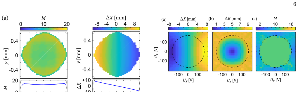
The central object is a stack of electrodes — a segmented extractor, a conical electrostatic lens, a segmented drift-tube deflector, and a 2x2 channel-electron-multiplier array — whose operation rests on a multipole decomposition of the potential on each four-segment electrode: the monopole term U, the dipole terms $U_X$ and $U_Y$, and the quadrupole term $U_{QP}$. The monopole creates the principal lensing effect through the radial field $\vec{E}_r \sim -\frac{r}{2}\frac{dE_z}{dz}\vec{e}_r$; the dipole shifts the beam and compensates stray fields; and the quadrupole produces strong single-axis magnification and effective image rotation. This segmentation is what lets one compact device both image and actively steer the ion trajectories onto individual CEMs.
What would settle it
Build the device and field-ionize rubidium atoms at known positions 100 micrometers below the chip surface, then measure the CEM hit coordinates and compare the resulting magnification with the predicted M = 12.25 at the standard voltages; a disagreement larger than the simulated depth-of-field and aberration spread, or a failure to resolve two atoms separated by about 2 micrometers under the quadrupole setting, would refute the central claim.
Extended reading notes
Core claim
The paper's central claim is that segmenting the extraction and deflection electrodes into four independently voltage-controlled quadrants gives complete multipole control over the ion trajectories, so a single 28 mm-diameter, 83 mm-long assembly can compensate stray electric fields, shift and enlarge the extraction region, rotate the image, and magnify along one axis by a factor of about 203 while keeping the perpendicular magnification below 3.2. At the standard working point, the simulated total magnification is M = 12.25, rising toward the edges of the detection plane, and applying a quadrupole voltage to the deflector electrodes produces the extreme single-axis stretching. The same electrode system can detect either ions or electrons, since charged particles follow identical trajectories under inverted voltages, and the paper shows that detecting both the electron and the ion from one ionization event gives a direct calibration of each CEM's detection efficiency.
Load-bearing premise
The quoted magnifications, extraction regions, and 2-micrometer resolution rest on the assumption that the simulated finite-difference fields of the idealized electrode geometry match the real device, including the assumed 100-micrometer starting distance and negligible initial ion energy spread.
Editorial extensions
If this is right
- Two Rydberg atoms separated by about 2 micrometers could be read out in parallel using the single-axis magnification, enabling correlation measurements on length scales relevant to Rydberg-blockade and cavity-mediated gates.
- The same electrode segments can cancel stray electric fields at the atoms, with simulated compensation strengths of 2.2 V/cm per volt axially and 26.5 mV/cm per volt laterally, which directly protects Rydberg-state fidelity.
- Detecting electron and ion from the same ionization event yields a per-detector efficiency calibration, so gate fidelities could be measured without requiring an independent, known detection efficiency.
- Because ion and electron trajectories are identical under inverted voltages, the detector can be switched between a slower ion mode and a nanosecond-timescale electron mode with the same imaging optics.
- All components fit within a compact, grounded tube that can be installed in an existing atom-chip vacuum apparatus, making the design a practical retrofit for current Rydberg experiments.
Reading between the lines
- The multipole-segmentation control scheme is not tied to this specific geometry; a similar four-quadrant electrode arrangement could give other atom-chip or MCP-based detectors the same image-rotation, stretching, and stray-field-compensation tools.
- If the simulated single-axis magnification is confirmed experimentally, the roughly 2-micrometer resolved separation would beat typical optical imaging limits for Rydberg arrays, which would directly help dense qubit geometries that current fluorescence imaging struggles to resolve.
- The electron-ion coincidence calibration, although presented as an efficiency measurement, also provides a per-shot check of whether exactly one atom was ionized; extending it to multi-atom events could distinguish genuine correlated pair detections from background counts.
- The dynamic voltage switching the paper lists as an outlook could turn the same electrodes into a time-dependent velocity or energy filter, potentially discriminating Rydberg states by their ionization energy rather than only by static field ionization.
Signed reviews
Editorial analysis
A structured set of objections, weighed in public.
Referee Report
Summary. This manuscript presents the design and simulation-based characterization of a compact electrostatic imaging and detection system for state-selective, spatially resolved readout of individual Rydberg atoms trapped near an atom chip. The device combines a segmented extraction electrode, a conical electrostatic lens, a segmented drift tube, and a 2x2 array of channel electron multipliers. Using SIMION trajectory simulations, the authors report a total magnification of about 12.25 at the chosen working point, a single-axis magnification up to about 203 using a quadrupole term on the deflector electrodes, a tunable extraction region, compensation of stray fields, and a coincidence-based scheme for calibrating detection efficiency using electron-ion pairs from the same ionization event.
Significance. If the simulated performance transfers to a fabricated device, this would be a useful contribution to Rydberg-atom quantum information platforms that require simultaneous, spatially resolved detection of multiple atoms. The multipole decomposition of the segmented electrodes is a clear and pedagogically valuable framework, and the electron-ion coincidence calibration scheme is a practical and well-motivated idea. The paper is also honest in labeling its central results as simulation-based, and it gives reproducible voltage settings and a concrete geometry. Its main value is as a design study that identifies a promising path toward compact correlation detection; the headline performance numbers, however, are not yet experimentally validated.
major comments (4)
- [III C, Fig. 7] The single-axis magnification Mx ≈ 203 is obtained at UQP/Udt = 0.35, which lies on the steep part of the Mx-versus-voltage curve. The paper provides no tolerance or sensitivity analysis for this working point. Small asymmetries among the four deflector segments, voltage drifts, or electrode misalignment will shift ion landing positions by amounts that could be comparable to the 400 µm CEM gap. Because the claim that particles separated by about 2 µm can be resolved depends directly on this extreme working point, the authors should quantify the sensitivity of Mx and of the landing coordinates to realistic voltage tolerances and mechanical misalignments, or explicitly label the result as a best-case ideal-geometry simulation.
- [IV, especially IV A and IV C] The abstract and conclusion claim that the imaging system maintains 'low aberrations' and images with 'minimal aberrations,' but the manuscript provides no quantitative aberration characterization. Section IV discusses spherical aberration, chromatic aberration, and depth of field only qualitatively, and it explicitly states that imaging quality in terms of resolution and sharpness is of secondary importance. There is no simulated spot size, point-spread function, rms blur, or distortion residual at the working point. The 'low aberrations' assertion should either be backed by quantitative simulation data or removed from the abstract and conclusion.
- [III B and II A] The extraction region is defined by treating particles that 'enter the deflector region' as detectable, but actual detection requires the ion to land on the active area of a CEM. Section II A itself warns that detection efficiency near CEM edges is strongly reduced, and the 400 µm gaps between CEMs are dead areas. The estimate that the single-axis magnification allows detection of particles separated by about 2 µm essentially assumes point-like spots placed across the CEM gap. The detection criterion used for the extraction-region and resolvable-separation claims should include the CEM active-area geometry and edge-efficiency effects, or the claims should be rephrased as addressing only the ion-optical transport rather than the full detection probability.
- [II C and III] All performance numbers come from SIMION simulations of an ideal electrode geometry with no experimental validation, no mesh-convergence study, and no discussion of patch potentials, surface charges, or insulator charging. These effects are particularly relevant near an atom chip, where adsorbate fields are known to be significant, and the paper's own Section II E acknowledges the need for stray-field compensation. The authors should add a limitations paragraph stating that the quoted magnifications, extraction regions, and deflection linearities are ideal-simulation predictions and that no statement about real-device accuracy is implied without further validation.
minor comments (6)
- [Fig. 10] The axis labels in Figure 10 appear corrupted by an encoding error (e.g., '/X30/X2D/X34' and similar strings). These must be replaced with the intended text such as 'x [mm]' and 'y [mm]'.
- [III A] The text says the maximal magnification amounts to 16 and then states that breakdown constraints yield a maximal magnification of about 12. This is confusing; please clarify that 16 is the unconstrained simulation maximum while about 12 is the maximum consistent with the stated voltage-breakdown limits.
- [IV C] The sentence 'At a distance of 2 mm this increase reaches an absolute value of 3' is ambiguous: it should state whether the magnification increases by 3 or to a value of 3 at 2 mm, and whether this is relative to the value at 100 µm.
- [II A] The CEM output voltage is described as 'typically set to −100 V for ion detection' with a potential difference of 100 V guiding the electron pulse to a grounded anode; the sign convention should be stated more carefully to avoid confusion about which electrode is at −100 V.
- [References] References [33] and [34] are manufacturer website URLs without document titles, part numbers, or access dates; for reproducibility these should be replaced by formal data-sheet citations or supplemented with retrieval dates.
- [Abstract] The phrase 'maintaining low aberrations' overstates what the paper demonstrates; if the quantitative aberration analysis is not added, the abstract should say that aberrations are discussed qualitatively or that the system is designed to minimize them.
Circularity Check
No significant circularity: the magnification and trajectory-control numbers are direct charged-particle simulation outputs, not fitted parameters or self-referential definitions, and the coincidence calibration is a standard conditional-probability identity.
full rationale
The paper's central performance claims are simulation outputs, not quantities defined in terms of themselves. In Sec. III A the magnification is explicitly 'given by the ratio of the particle separation at the imaging plane to the initial separation,' and the values M = 12.25 and Mx ≈ 203 are computed from SIMION trajectories for stated voltages (Uext = -50 V, Ucon = -1000 V, Udt = -2000 V, UQP = -700 V). This is a direct trajectory-simulation readout, not a fit to the headline claim. The single-axis magnification study in Sec. III C likewise reports simulated Mx and My as functions of UQP/Udt; no parameter is adjusted to reproduce the claimed result after the fact. The coincidence calibration in Sec. V rests on the standard identity that, for a correlated electron-ion pair, the conditional probability of detecting the ion given electron detection equals the ion detection efficiency; this is an external, mathematically simple method and is cited to prior work, but it is not a load-bearing self-citation that defines the detector's claimed capability. The self-citations present ([15], [23], [31], [46], [51]) provide background on atom-chip trapping, stray fields, ionization energy spreads, and coincidence methods; none is invoked as a uniqueness theorem or as the sole justification for an otherwise unsupported premise. The main caveats are experimental fidelity of the idealized SIMION geometry, lack of tolerance or aberration quantification, and the steepness of the Mx versus UQP characteristic near the working point; these are correctness or validation risks, not circularity. The derivation chain is therefore self-contained with respect to circularity, and the honest finding is no significant circularity.
Assumptions & free parameters
free parameters (4)
- Ion detection operating voltages =
Uext=-50 V, Ucon=-1000 V, Udt=-2000 V, UCEM=-2300 V
- Extractor dipole voltage ratio =
UXY=0.23 Uext (-11.5 V)
- Deflector quadrupole voltage =
UQP=-700 V (UQP/Udt=0.35)
- Particle starting distance =
100 µm below chip surface
assumptions (5)
- domain assumption SIMION finite-difference solutions of Laplace's equation accurately represent the real electrode fields and ion trajectories.
- domain assumption Charged particles follow identical trajectories in an electrostatic field when voltages are inverted, independent of mass when initial velocities are negligible.
- domain assumption CEM detection efficiency exceeds 50% for ions above 2 keV and electrons above 20 eV, as per manufacturer data.
- domain assumption Rydberg atoms can be field-ionized near the chip and ions start at 100 µm below the surface with negligible energy spread.
- ad hoc to paper Particles entering the deflector region are considered detectable, defining the extraction region.
Cite this review
Pith. "Pith review of Compact detector for atom-atom correlations on an atom chip." pith.science (2026). https://pith.science/paper/KO4V7LA4
@misc{pith2026250703624,
  author       = {Pith},
  title        = {Pith review of: Compact detector for atom-atom correlations on an atom chip},
  year         = {2026},
  howpublished = {\url{https://pith.science/paper/KO4V7LA4}},
  note         = {Machine review of arXiv:2507.03624}
}
read the original abstract
We present a compact, ionization-based detector for the state-selective and spatially resolved measurement of individual Rydberg atoms trapped in the vicinity of an atom chip. The system combines an electrostatic lens system for guiding charged particles with an array of channel electron multipliers (CEMs) capable of detecting both ions and electrons produced by ionization. Designed for quantum information applications, this device enables the detection of correlations between spatially separated Rydberg qubits. Additionally, the electrodes provide compensation for stray electric fields and control over particle trajectories. The imaging system achieves a total magnification of more than 12, with a single-axis magnification up to 200, while maintaining low aberrations. We characterize the performance of the system using a charged particle trajectory simulation software and discuss how a coincidence measurement of ions and electrons can be used to calibrate the detection efficiency. This detector enables high-fidelity measurement of multiple Rydberg atoms and is well-suited for applications in cavity-mediated quantum gates.
Figures


Figures from the paper (7 more)


Reference graph
Works this paper leans on
-
[1]
T. F. Gallagher, in Springer Handbook of Atomic, Molec- ular, and Optical Physics(Springer, 1994) pp. 231–240
work page 1994
-
[2]
M. D. Lukin, M. Fleischhauer, R. Cote, L. Duan, D. Jaksch, J. I. Cirac, and P. Zoller, Physical review let- ters 87, 037901 (2001)
work page 2001
-
[3]
M. Saffman, T. G. Walker, and K. Mølmer, Reviews of modern physics 82, 2313 (2010)
work page 2010
-
[4]
A. M. Kaufman and K.-K. Ni, Nature Physics 17, 1324 (2021)
work page 2021
-
[5]
Bluvstein, H
D. Bluvstein, H. Levine, G. Semeghini, T. T. Wang, S. Ebadi, M. Kalinowski, A. Keesling, N. Maskara, H. Pichler, M. Greiner, et al., Nature 604, 451 (2022)
2022
- [6]
-
[7]
Scholl, M
P. Scholl, M. Schuler, H. J. Williams, A. A. Eberharter, D. Barredo, K.-N. Schymik, V. Lienhard, L.-P. Henry, T. C. Lang, T. Lahaye, et al., Nature 595, 233 (2021)
2021
- [8]
Show all 52 references
-
[9]
C. Chen, G. Bornet, M. Bintz, G. Emperauger, L. Leclerc, V. S. Liu, P. Scholl, D. Barredo, J. Hauschild, S. Chatterjee, et al., Nature 616, 691 (2023)
2023
-
[10]
Schauß, J
P. Schauß, J. Zeiher, T. Fukuhara, S. Hild, M. Cheneau, T. Macr ` ı, T. Pohl, I. Bloch, and C. Groß, Science 347, 1455 (2015)
2015
-
[11]
Labuhn, D
H. Labuhn, D. Barredo, S. Ravets, S. De L´ es´ eleuc, T. Macr ` ı, T. Lahaye, and A. Browaeys, Nature534, 667 (2016)
2016
-
[12]
Bernien, S
H. Bernien, S. Schwartz, A. Keesling, H. Levine, A. Om- ran, H. Pichler, S. Choi, A. S. Zibrov, M. Endres, M. Greiner, et al., Nature 551, 579 (2017)
2017
-
[13]
Stammeier, S
M. Stammeier, S. Garc ´ ıa, T. Thiele, J. Deiglmayr, J. A. Agner, H. Schmutz, F. Merkt, and A. Wallraff, Physical Review A 95, 053855 (2017)
2017
-
[14]
Morgan and S
A. Morgan and S. Hogan, Physical Review Letters 124, 193604 (2020)
2020
-
[15]
Kaiser, C
M. Kaiser, C. Glaser, L. Y. Ley, J. Grimmel, H. Hatter- mann, D. Bothner, D. Koelle, R. Kleiner, D. Petrosyan, A. G¨ unther,et al., Physical Review Research 4, 013207 (2022)
2022
-
[16]
J. M. Kondo, S. T. Rittenhouse, D. V. Magalhaes, V. Rokaj, S. I. Mistakidis, H. R. Sadeghpour, and L. G. Marcassa, Physical Review A 110, L061301 (2024)
2024
-
[17]
J. D. Pritchard, D. Maxwell, A. Gauguet, K. J. Weath- erill, M. Jones, and C. S. Adams, Physical review letters 105, 193603 (2010)
2010
-
[18]
J. D. Pritchard, K. J. Weatherill, and C. S. Adams, An- nual Review of Cold Atoms and Molecules: Volume 1 , 301 (2013)
2013
-
[19]
Karlewski, M
F. Karlewski, M. Mack, J. Grimmel, N. S´ andor, and J. Fort´ agh, Physical Review A91, 043422 (2015)
2015
-
[20]
Gallagher, L
T. Gallagher, L. Humphrey, W. Cooke, R. Hill, and S. Edelstein, Physical Review A 16, 1098 (1977)
1977
-
[21]
van Ditzhuijzen, A
C. van Ditzhuijzen, A. Koenderink, L. Noordam, and H. van Linden van den Heuvell, The European Physi- cal Journal D-Atomic, Molecular, Optical and Plasma Physics 40, 13 (2006)
2006
-
[22]
V. C. Gregoric, J. J. Bennett, B. R. Gualtieri, A. Kannad, Z. C. Liu, Z. A. Rowley, T. J. Carroll, and M. W. Noel, Physical Review A 98, 063404 (2018)
2018
-
[23]
Fort´ agh and C
J. Fort´ agh and C. Zimmermann, Reviews of Modern Physics 79, 235 (2007)
2007
-
[24]
Drummond, Vacuum 34, 51 (1984)
I. Drummond, Vacuum 34, 51 (1984)
1984
-
[25]
O. Sise, M. Ulu, and M. Dogan, Nuclear Instruments and Methods in Physics Research Section A: Acceler- ators, Spectrometers, Detectors and Associated Equip- ment 573, 329 (2007)
2007
-
[26]
El-Kareh and M
A. El-Kareh and M. Sturans, Journal of Applied Physics 42, 1870 (1971)
1971
-
[27]
Adams and F
A. Adams and F. Read, Journal of Physics E: Scientific Instruments 5, 150 (1972)
1972
-
[28]
J. M. McGuirk, D. M. Harber, J. M. Obrecht, and E. A. Cornell, Phys. Rev. A 69, 062905 (2004)
2004
-
[29]
J. M. Obrecht, R. J. Wild, M. Antezza, L. P. Pitaevskii, S. Stringari, and E. A. Cornell, Phys. Rev. Lett. 98, 063201 (2007)
2007
-
[30]
Tauschinsky, R
A. Tauschinsky, R. M. T. Thijssen, S. Whitlock, H. B. van Linden van den Heuvell, and R. J. C. Spreeuw, Phys. Rev. A 81, 063411 (2010)
2010
-
[31]
Hattermann, M
H. Hattermann, M. Mack, F. Karlewski, F. Jessen, D. Cano, and J. Fort´ agh, Phys. Rev. A86, 022511 (2012)
2012
-
[32]
K. Chan, M. Siercke, C. Hufnagel, and R. Dumke, Phys- ical review letters 112, 026101 (2014)
2014
-
[33]
Sjuts Optotechnik GmbH, www.sjuts.com
Dr. Sjuts Optotechnik GmbH, www.sjuts.com
-
[34]
SwabianInstruments, www.swabianinstruments.com
-
[35]
Henkel, Photoionisation detection of single 87Rb- atoms using channel electron multipliers, Ph.D
F. Henkel, Photoionisation detection of single 87Rb- atoms using channel electron multipliers, Ph.D. thesis, Ludwing-Maximilians-University Munich (2011). 12
2011
-
[36]
J. L. Wiza et al., Nucl. Instrum. Methods 162, 587 (1979)
1979
-
[37]
Lampton and R
M. Lampton and R. Malina, Review of Scientific Instru- ments 47, 1360 (1976)
1976
-
[38]
O. H. Siegmund, A. S. Tremsin, J. V. Vallerga, and J. Hull, IEEE Transactions on Nuclear Science 48, 430 (2001)
2001
-
[39]
Keller, G
H. Keller, G. Klingelh¨ ofer, and E. Kankeleit, Nuclear In- struments and Methods in Physics Research Section A: Accelerators, Spectrometers, Detectors and Associated Equipment 258, 221 (1987)
1987
-
[40]
Jagutzki, A
O. Jagutzki, A. Cerezo, A. Czasch, R. Dorner, M. Hattas, M. Huang, V. Mergel, U. Spillmann, K. Ullmann-Pfleger, T. Weber, et al., IEEE Transactions on Nuclear Science 49, 2477 (2002)
2002
-
[41]
Both, PEEK and MA- COR, feature a dielectric strength above 20 kV/mm [24], which is negligible compared to the vacuum breakdown voltage and insulator surface effects
and is not suitable for vacuum applications, such that MACOR would be used instead. Both, PEEK and MA- COR, feature a dielectric strength above 20 kV/mm [24], which is negligible compared to the vacuum breakdown voltage and insulator surface effects. In an ultrahigh vac- uum c...
-
[42]
S. Z. Cheng, M. Cao, and B. Wunderlich, Macromolecules 19, 1868 (1986)
1986
-
[43]
Bergmann and C
L. Bergmann and C. Schaefer, Optik: Wellen-und Teilchenoptik (Walter de Gruyter, 2004)
2004
-
[44]
H¨ ytch and P
M. H¨ ytch and P. W. Hawkes, Quadrupoles in electron lens design, Vol. 224 (Academic Press, 2022)
2022
-
[45]
Scherzer, Zeitschrift f¨ ur Physik101.9-10, 51 (1936)
O. Scherzer, Zeitschrift f¨ ur Physik101.9-10, 51 (1936)
1936
-
[46]
Szilagyi, Applied physics letters 49, 767 (1986)
M. Szilagyi, Applied physics letters 49, 767 (1986)
1986
-
[47]
Stecker, H
M. Stecker, H. Schefzyk, J. Fort´ agh, and A. G¨ unther, New Journal of Physics 19, 043020 (2017)
2017
-
[48]
Tiesinga, B
E. Tiesinga, B. Verhaar, and H. Stoof, Physical Review A 47, 4114 (1993)
1993
-
[49]
Inouye, M
S. Inouye, M. Andrews, J. Stenger, H.-J. Miesner, D. Stamper-Kurn, and W. Ketterle, Nature 392, 151 (1998)
1998
-
[50]
Courteille, R
P. Courteille, R. Freeland, D. Heinzen, F. Van Abeelen, and B. Verhaar, Physical Review Letters 81, 69 (1998)
1998
-
[51]
C. Chin, R. Grimm, P. Julienne, and E. Tiesinga, Re- views of Modern Physics 82, 1225 (2010)
2010
-
[52]
Stibor, S
A. Stibor, S. Kraft, T. Campey, D. Komma, A. G¨ unther, J. Fort´ agh, C. Vale, H. Rubinsztein-Dunlop, and C. Zim- mermann, Physical Review A 76, 033614 (2007)
2007
Reviewed August 6, 2026 · model on record in the stance chip above.
Discussion (0). Continue with ORCID to comment.