REVIEW 4 major objections 6 minor 26 references
A Practical Flake Segmentation and Indexing Pipeline for Automated 2D Material Stacking
T0 review · 4 major / 6 minor · reviewed 2026-08-05 · deepseek-v4-flash
Pith's one-line read A $35k pipeline can scan a 3-inch wafer, segment more than 6,000 valid 2D-material subflakes, and assign thicknesses from optical color alone.
desk verdict A genuinely useful automation pipeline whose headline precision claim is undermined by circular validation and missing error bars. read the letter →
The pith
A machine-rendered reading of the paper's core claim, the machinery that carries it, and where it could break.
The reading
What carries the argument
The central object is the AFM-calibrated RGB-thickness curve on a 285 nm SiO2/Si substrate—the lookup table that connects a segment's average color to a physical layer count via thin-film interference—together with a flake-first two-stage segmentation: first Canny/color-threshold detection with geometric filters to isolate flakes, then per-flake k-means clustering in RGB space with transitive color-distance merging to define 'subflakes' (uniform-thickness domains). The color-match acceptance against the calibration curve is what filters out tape residue, dust, and polymer contamination.
What would settle it
Take a random sample of the segmented subflakes from the reported 3-inch wafer, verify them non-destructively with AFM, and count the spurious fraction; if it is not below 1%, the >99% validity claim fails. A second test: run the unchanged pipeline and thresholds on a different-batch 285 nm SiO2/Si wafer under the same illumination, and check whether the graphene 1-8 layer R-G clusters stay disjoint; if they overlap, the claimed transferability and layer-assignment reliability fail.
Extended reading notes
Core claim
The paper claims to turn raw optical images of an exfoliated 3-inch wafer into a searchable database of flakes and thickness domains using less than $35k of hardware. Flake detection is precision-first: hBN via Canny edge detection on a red-channel contrast transform, graphene via color thresholding plus filters on area, complexity, solidity, and extent that reject dust and tape residue. Each flake is then clustered by k-means in RGB space; adjacent clusters merge when close in color, and a component is accepted as a subflake only if its mean color matches an AFM-calibrated RGB-thickness curve within tolerance. On a full wafer the pipeline found over 6,000 valid subflakes in under 12 hours,
Load-bearing premise
The pipeline assumes that the AFM-calibrated RGB-to-thickness curve and the fixed thresholds (RGB selection ranges, area, complexity, solidity, extent, k, merge distance) transfer from this specific 285 nm SiO2/Si wafer, illumination, and camera settings to any other wafer, material, or microscope without re-tuning.
Editorial extensions
If this is right
- A full 3-inch exfoliation run can be converted in under 12 hours into a searchable flake library, removing the manual-hunting step from heterostructure fabrication.
- Graphene layer counts from one to eight can be read off from optical color alone, making routine AFM or Raman screening unnecessary for candidate selection.
- The exported database entries (centroid, inner/outer rectangle, average RGB, thickness) can directly drive robotic pick-up and stacking, so the imaging step stops being a bottleneck.
- Mixed-material exfoliation on one wafer becomes practical, since the lightweight classifier detects the flake type and switches to the optimal lighting condition automatically.
Reading between the lines
- If the RGB-thickness calibration transfers, the same two-stage scheme could be applied to other interference substrates (e.g., 90 nm SiO2 or encapsulated wafers) simply by recalibrating the lookup table, an inexpensive route to automated exfoliation screening in other material families.
- The reported disjoint 1-8 layer R-G clusters imply that a simple nearest-centroid classifier could replace the k-means step for thickness assignment on this substrate, further lowering the annotation burden.
- An explicit false-positive audit per artifact class (tape vs dust vs polymer contamination) would make the >99% validity claim reproducible across batches, since the denominator depends on manually chosen thresholds.
- Extending the Stack Designer .stk format with uncertainty estimates for thickness could let robotic stacking tolerate ambiguous-color flakes, broadening automated assembly beyond the well-separated clusters.
Signed reviews
Editorial analysis
A structured set of objections, weighed in public.
Referee Report
Summary. The paper describes a modular optical-microscopy pipeline for automated detection, segmentation, and thickness indexing of exfoliated 2D material flakes on 285 nm SiO₂/Si wafers. It combines a CNN-based field-of-view classifier, Canny/color-based flake segmentation, k-means subflake segmentation with RGB merge criteria, an AFM-calibrated RGB–thickness lookup, and a structured database with stack-design tools. The authors report scanning a full 3-inch wafer in under 12 hours, identifying over 6,000 valid subflakes, with over 99% of segmented subflakes corresponding to real 2D material features, and claim rapid thickness assignment without AFM or Raman.
Significance. If its quantitative claims are supported, this would be a practically valuable systems contribution: it is hardware-light, avoids deep-learning-based segmentation, and produces structured output directly usable for automated stacking. The two-stage, flake-first segmentation design is transparent and interpretable, and the demonstration on a full wafer is impressive. The main weakness is that the headline precision and thickness-assignment claims currently rest on circular validation: subflakes are accepted only when their RGB matches the AFM-calibrated curve, and the same filter is used to claim >99% validity. With independent, wafer-scale validation, the approach could be an important enabling tool for automated van der Waals assembly.
major comments (4)
- [Subflake Segmentation by Thickness Contrast / A structured flake database] A component is accepted as a subflake 'only if its average color matches a known flake thickness within a specified RGB deviation threshold' using the same AFM-calibrated RGB–thickness mapping. The later claim, 'Over 99% of the segmented subflakes correspond to actual 2D material features,' is presented without describing how this was measured. If this figure is derived from the acceptance filter itself, the claim is tautological: the filter guarantees the color match regardless of whether the region is a real flake. Please report the exact validation protocol (manual inspection, AFM, Raman, or other), the number of subflakes inspected, and the false-positive/false-negative counts. Without this, the >99% validity claim is not falsifiable as stated.
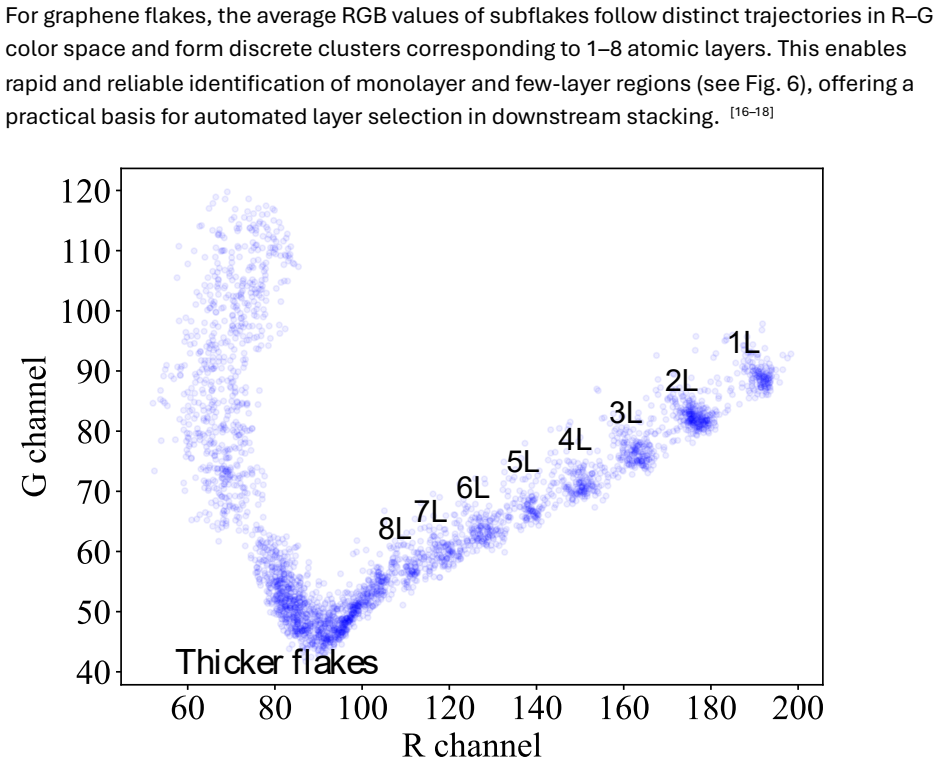
- [Figure 5 and thickness assignment] The well-separated R–G clusters labeled 1–8 layers in Figure 5 are obtained from subflakes that have already passed the RGB-matching acceptance criterion, so the figure does not independently validate the thickness assignment. The only external checks are Raman spectra at three points on one graphene flake and AFM on one hBN flake. This is too sparse to establish wafer-scale precision or the claim of 'rapid and reliable thickness assignment without nanoscale measurements.' Please provide independent thickness verification (e.g., AFM/Raman) on a random sample of subflakes across the wafer, with error statistics such as mean absolute error and a confusion matrix for layer assignment.
- [Image Acquisition and Classifications] The statement 'over 98% classification accuracy, with no observed confusion between graphene, hBN, and TMD categories' is not accompanied by dataset size, class distribution, train/test split, or confidence intervals. Since the CNN classifier gates all downstream processing, this claim needs proper quantitative support. Please report the number of images per class, the validation methodology, and the confusion matrix. 'No observed confusion' is not meaningful without sample sizes.
- [Flake Segmentation from Optical Images / Subflake Segmentation] The pipeline depends on many hand-tuned thresholds: color range 45 < R < 198, G < 140 (as written, 'G < 14' appears to be a typo), geometric filters (area, complexity < 25, solidity > 0.4, extent > 0.2), k-Means k = 11/21, merge thresholds 2 and 4, and the RGB deviation threshold for subflake acceptance. The abstract claims 'rapid deployment across diverse 2D material systems and imaging conditions,' but only a single substrate and illumination condition are demonstrated. Please provide a sensitivity analysis for the main thresholds, or explicitly state the transferability limitations. As written, the portability claim is not supported.
minor comments (6)
- [Flake Segmentation from Optical Images] The color threshold is given as 'G < 14' in the main text but 'G < 140' in the Figure 2 caption. This is likely a typo; please correct.
- [Image Acquisition and Classifications] The field of view is stated as '40 μm×440 μm'; this appears to be a typo, likely '400 μm × 440 μm' or similar. Please verify.
- [Flake Segmentation from Optical Images] The section heading 'Flake egmentation' is missing an 'S'. Also, the Canny parameters 'cv2.Canny(r_diff, 30, 72)' appear only in the Figure 2 caption; they should be stated in the methods text.
- [Image Acquisition and Classifications] The CNN architecture, training data, and hyperparameters are only referenced as Supplementary Information 2. Since the classifier is load-bearing, include at least a brief architecture/training summary in the main text.
- [Figure 4 and structured database] The table entries in Figure 4 appear with garbled or missing separators (e.g., 'Flake ID=2' rows). Please ensure the CSV representation is clean and readable.
- [References] Reference 25 duplicates reference 9 (Wang et al., Electronics and optoelectronics...). Remove the duplicate.
Circularity Check
The >99% subflake-validity and thickness-assignment claims reduce to the AFM-calibrated RGB acceptance filter as described; no independent wafer-scale validation is reported.
-
fitted input called prediction
[Subflake Segmentation by Thickness Contrast; Fig. 5 caption]
"For each retained region, we compute the average RGB value from the de-vignetted image, and compare it against a pre-established RGB–thickness calibration curve (obtained via AFM). A component is accepted as a subflake only if its average color matches a known flake thickness within a specified RGB deviation threshold. ... This separation validates the effectiveness of our segmentation and indexing pipeline for layer-selective device design."
The subflake set is defined by accepting components whose average RGB matches the AFM-calibrated RGB–thickness curve. The thickness labels assigned to those subflakes are therefore read off the same fitted curve. Figure 5's 'discrete clusters' of R–G values for 1–8 layers are a consequence of this acceptance filter and the calibration curve, not an independent confirmation that those colors correspond to those layer numbers. The only external checks (Raman at three points, AFM on one hBN flake) cover a tiny fraction of the >6,000 subflakes, so the wafer-scale 'rapid and reliable thickness assignment' is not independently verified.
-
self definitional
[A structured flake database, full-wafer application paragraph]
"In total, over 6,000 valid subflakes were identified across the wafer. Over 99% of the segmented subflakes correspond to actual 2D material features, rather than spurious artifacts such as tape residue, polymer contamination, or dust particles."
The paper does not describe any independent method for measuring this 99% precision statistic. The only acceptance rule described earlier is the AFM-calibrated RGB–thickness color match, which is precisely the filter that defines 'segmented subflakes.' If the 99% figure is evaluated on the output of that filter, then it is guaranteed by construction that accepted components resemble known flake thicknesses; it does not establish that they are 'actual 2D material features.' As reported, the headline precision claim reduces to the acceptance criterion rather than being validated against external ground truth.
full rationale
The pipeline's core segmentation mechanics (Canny edges, k-means clustering, geometric filters) are not circular, and the AFM calibration is a legitimate external input. However, the two central quantitative claims—thickness assignment for >6,000 subflakes and >99% precision—are presented as validated by the same color-matching rule that creates the subflake set. The paper provides only three Raman points and one AFM topography as external checks, which are too sparse to support wafer-scale precision. Thus, as written, the central validation is partially circular: accepted subflakes match the calibration curve by definition, and no independent precision measurement is reported. This warrants a score of 6 rather than a higher score because the underlying pipeline could in principle be validated externally, and some independent spot checks are shown.
Assumptions & free parameters
free parameters (7)
- Graphene color thresholds =
45 < R < 198, G < 140
- Geometric filters =
area > 5 um2, complexity < 25, solidity > 0.4, extent > 0.2
- Canny thresholds for hBN =
cv2.Canny(r_diff, 30, 72)
- k-Means cluster count k =
21 for hBN, 11 for graphene
- RGB merge thresholds =
2 for hBN, 4 for graphene
- AFM-derived RGB-thickness calibration curve =
curve values not given numerically
- Subflake component area threshold =
5 um x 5 um bounding square
assumptions (4)
- domain assumption Optical color on 285 nm SiO2/Si is a deterministic, monotonic function of flake thickness via thin-film interference.
- domain assumption The AFM-calibrated RGB-thickness mapping is valid and transferable within a wafer and across batches.
- domain assumption The CNN classifier trained on manually annotated images generalizes across illumination and wafer variations.
- ad hoc to paper Hand-tuned geometric and color thresholds are portable across imaging conditions.
Cite this review
Pith. "Pith review of A Practical Flake Segmentation and Indexing Pipeline for Automated 2D Material Stacking." pith.science (2026). https://pith.science/paper/BDM6PCN5
@misc{pith2026250901826,
  author       = {Pith},
  title        = {Pith review of: A Practical Flake Segmentation and Indexing Pipeline for Automated 2D Material Stacking},
  year         = {2026},
  howpublished = {\url{https://pith.science/paper/BDM6PCN5}},
  note         = {Machine review of arXiv:2509.01826}
}
read the original abstract
A cost-effective and robust image-processing pipeline is presented for the detection and characterization of exfoliated two-dimensional (2D) material flakes in optical microscope images, designed to facilitate automation in van der Waals heterostructure assembly. The system combines shallow machine learning (ML)-based material classification with a precision-first flake detection algorithm driven by edge morphology and color discontinuity. Step edges are resolved when supported by optical contrast, while spurious features such as dust and background texture are reliably rejected. Each identified flake is exported in a structured format that includes centroid coordinates, bounding geometries, average RGB color, and estimated optical thickness, enabling seamless integration into automated pick-up and stacking workflows. The pipeline is hardware-light and operates without the need for deep learning models or nanoscale ground-truth labels, making it practical for scalable front-end wafer processing at a hardware cost of under 30,000 USD. In contrast to prior approaches that focus solely on detection accuracy, the proposed system unifies flake segmentation with indexing, filtering, and blueprint-driven stacking, forming a closed-loop workflow from image acquisition to device planning. Its low annotation requirement and flexible implementation enable rapid deployment across diverse 2D material systems and imaging conditions.
Figures


Figures from the paper (1 more)
Reference graph
Works this paper leans on
-
[1]
Department of Condensed Matter Physics and Materials Science, Brookhaven National Laboratory, Upton NY, 11973
-
[2]
Department of Physics, Columbia University, New York, NY, 10027 #. Corresponding author Keywords: 2D materials, flake segmentation, optical microscopy, laboratory automation, machine learning, image processing, step edge detection Abstract: A cost-effective and robust image-processing pipeline is presented for the detection and characterization of exfolia...
-
[3]
Minimum area (> 5 μm²) — to exclude noise and extremely small features
-
[4]
Complexity (< 25) — defined as the perimeter divided by the square root of the area; this penalizes highly irregular shapes (e.g., dust) while preserving compact flake regions
-
[5]
olidity (> .4) — the ratio of region area to its convex hull area; this eliminates highly concave or fragmented shapes
-
[6]
Extent (> .2) — the ratio of region area to its bounding box area; this further excludes narrow or elongated noise artifacts. These criteria are intended to isolate genuine graphene flakes while filtering out spurious non-flake features. The area surrounding each retained region is then cropped and saved for subsequent subflake analysis. At this stage, a ...
- [7]
-
[8]
Emerging photoluminescence in monolayer MoS2
Splendiani, A., et al. Emerging photoluminescence in monolayer MoS2. Nano Letters 10, 1271–1275 (2010). https://doi.org/10.1021/nl9038 8w
Show all 26 references
-
[9]
Geim, A. K. & Grigorieva, I. V. Van der Waals heterostructures. Nature 499, 419–425 (2013). https://doi.org/10.1038/nature12385
2013 doi
-
[10]
S., et al
Novoselov, K. S., et al. 2D materials and van der Waals heterostructures. Science 353, aac9439 (201 ). https://doi.org/10.112 /science.aac9439
-
[11]
2D transition metal dichalcogenides
Manzeli, S., et al. 2D transition metal dichalcogenides. Nature Reviews Materials 2, 17033 (2017). https://doi.org/10.1038/natrevmats.2017.33 . Liu, Y., et al. Van der Waals heterostructures and devices. Nature Reviews Materials 1, 1 042 (201 ). https://doi.org/10.1038/natrevm...
2017 doi
-
[12]
R., et al
Dean, C. R., et al. Boron nitride substrates for high-quality graphene electronics. Nature Nanotechnology 5, 722–72 (2010). https://doi.org/10.1038/nnano.2010.172
2010 doi
-
[13]
Z., et al
Butler, S. Z., et al. Progress, challenges, and opportunities in two-dimensional materials beyond graphene. ACS Nano 7, 2898–292 (2013). https://doi.org/10.1021/nn400280c
2013 doi
-
[15]
Intelligent identification of two-dimensional nanostructures by machine- learning optical microscopy
Lin, X., et al. Intelligent identification of two-dimensional nanostructures by machine- learning optical microscopy. Nano Research 11, 311– 322 (2018). https://doi.org/10.1007/s12274-018-2155-0
2018 doi
-
[16]
Classifying optical microscope images of exfoliated graphene flakes by data-driven machine learning
Masubuchi, S., et al. Classifying optical microscope images of exfoliated graphene flakes by data-driven machine learning. npj 2D Materials and Applications 3, 4 (2019). https://doi.org/10.1038/s41 99-018-0084-0
2019 doi
-
[17]
Automated system for the detection of 2D materials using digital image processing and deep learning
Sanchez-Juarez, J., et al. Automated system for the detection of 2D materials using digital image processing and deep learning. Optical Materials Express 12, 1214–1232 (2022). https://doi.org/10.13 4/OME.448523
2022
-
[18]
M., et al
Sterbentz, R. M., et al. Universal image segmentation for optical identification of 2D materials. Scientific Reports 11, 5934 (2021). https://doi.org/10.1038/s41598-021-85159-9
2021 doi
-
[19]
Making graphene visible
Blake, P., et al. Making graphene visible. Applied Physics Letters 91, 0 3124 (2007). https://doi.org/10.10 3/1.27 8 24
2007
-
[20]
Graphene thickness determination using reflection and contrast spectroscopy
Ni, Z., et al. Graphene thickness determination using reflection and contrast spectroscopy. Nano Letters 7, 2758–27 3 (2007). https://doi.org/10.1021/nl071254m 1 . Jessen, B. S., et al. Quantitative optical mapping of two-dimensional materials. Scientific Reports 8, 381 (2018)...
2007 doi
-
[21]
Rapid and reliable thickness identification of two-dimensional nanosheets using optical microscopy
Li, H., et al. Rapid and reliable thickness identification of two-dimensional nanosheets using optical microscopy. ACS Nano 7, 10344–10353 (2013). https://doi.org/10.1021/nn4047474
2013 doi
-
[22]
Optical microscope based universal parameter for identifying layer number in two-dimensional materials
Mondal, M., et al. Optical microscope based universal parameter for identifying layer number in two-dimensional materials. ACS Nano 1 , 12933–12941 (2022). https://doi.org/10.1021/acsnano.2c04833
2022 doi
-
[23]
Autonomous robotic searching and assembly of two-dimensional crystals to build van der Waals superlattices
Masubuchi, S., et al. Autonomous robotic searching and assembly of two-dimensional crystals to build van der Waals superlattices. Nature Communications 9, 1413 (2018). https://doi.org/10.1038/s414 7-018-03723-w
2018 doi
-
[25]
J., et al
Zomer, P. J., et al. Fast pick up technique for high-quality heterostructures of bilayer graphene and hexagonal boron nitride. Applied Physics Letters 105, 013101 (2014). https://doi.org/10.10 3/1.488 09
2014
-
[27]
J., et al
McGilly, L. J., et al. Visualization of moiré superlattices. Nature Nanotechnology 15, 580–584 (2020). https://doi.org/10.1038/s415 5-020-0708-3
2020 doi
-
[28]
Graphene and Beyond: Recent Advances in Two-Dimensional Materials Synthesis, Properties, and Devices
Lei, Y., et al. Graphene and Beyond: Recent Advances in Two-Dimensional Materials Synthesis, Properties, and Devices. ACS Nanoscience Au 2, 112–142 (2022). https://doi.org/10.1021/acsnanoscienceau.2c00017
2022 doi
-
[29]
H., et al
Wang, Q. H., et al. Electronics and optoelectronics of two-dimensional transition metal dichalcogenides. Nature Nanotechnology 7, 99–712 (2012). https://doi.org/10.1038/nnano.2012.193 Table o Contents This article presents a robust, cost-effective image-processing pipeline for...
2012 doi
Reviewed August 5, 2026 · model on record in the stance chip above.
Discussion (0). Continue with ORCID to comment.