Highly Efficient Exciton Modulation in MoSe₂/PdSe₂ Heterostructures
Pith reviewed 2026-05-20 21:42 UTC · model grok-4.3
The pith
Interlayer electronic coupling in MoSe2/PdSe2 heterostructures redistributes excitons to boost A-exciton emission sixfold.
A machine-rendered reading of the paper's core claim, the machinery that carries it, and where it could break.
Core claim
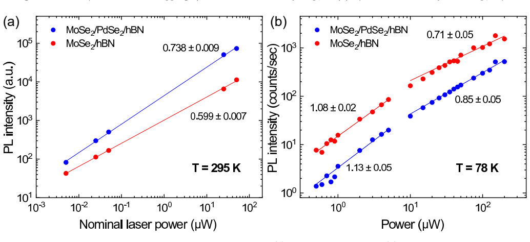
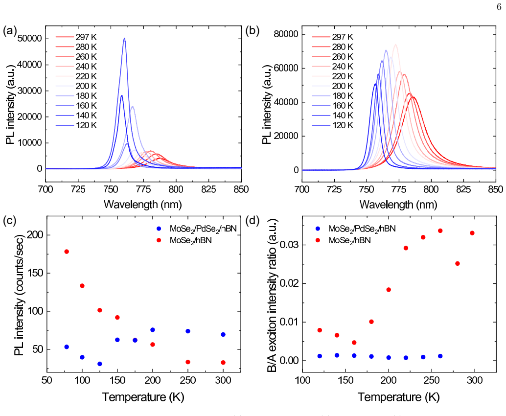
In the MoSe₂/PdSe₂ van der Waals heterostructure, interlayer electronic coupling redistributes exciton populations from the B-exciton to the lower-energy radiative A-exciton channel. This results in a pronounced enhancement of room-temperature A-exciton emission by a factor of approximately six, corresponding to a photoluminescence quantum yield of 6% compared to 1% in the isolated monolayer. Power-dependent measurements indicate reduced exciton-exciton annihilation, while temperature-dependent data show a crossover to quenched emission at low temperatures. Broadband photoluminescence excitation spectroscopy confirms the effect spans 450-725 nm, ruling out resonance-specific mechanisms.
What carries the argument
Interlayer electronic coupling in a type-I MoSe2/PdSe2 heterostructure that redistributes exciton populations toward the radiative A-exciton.
If this is right
- Interlayer coupling provides an efficient route to enhance emission efficiency in two-dimensional semiconductors without chemical modification or applied strain.
- Suppression of exciton-exciton annihilation occurs as a result of the population redistribution.
- The enhancement is broadband, applying across excitation wavelengths from 450 to 725 nm.
- Exciton relaxation pathways can be redirected at the van der Waals interface to favor radiative channels over non-radiative ones.
Where Pith is reading between the lines
- Similar coupling effects might improve performance in other transition metal dichalcogenide heterostructures for light-emitting applications.
- Interface engineering via such stacks could help overcome defect-related non-radiative losses in practical devices.
- Device designs could incorporate PdSe2 layers to modulate emission without altering the active MoSe2 material directly.
Load-bearing premise
The measured increase in photoluminescence directly indicates a higher quantum yield from exciton population redistribution rather than from altered absorption, interface defects, or experimental collection efficiency.
What would settle it
Direct measurement of the absorption cross-section in the heterostructure compared to the monolayer MoSe2 to determine if the emission boost matches the absorption change or exceeds it.
Figures



read the original abstract
Controlling exciton recombination in atomically thin semiconductors is central to their optoelectronic functionality, as the competition between radiative and non-radiative decay channels governs emission efficiency. Existing approaches, such as defect passivation, chemical doping, dielectric engineering, and strain tuning, primarily aim to suppress non-radiative losses. Here, we report a pronounced $\sim$6-fold enhancement of room-temperature A-exciton emission in a type-I MoSe$_2$/PdSe$_2$ van der Waals heterostructure, yielding a photoluminescence quantum yield of 6 %, compared to $\sim$1 % for as-exfoliated monolayer MoSe$_2$. This enhancement is accompanied by strong quenching of the B-exciton, consistent with interlayer electronic coupling that redistributes exciton populations toward the radiative A-exciton channel. Power- and temperature-dependent measurements reveal a suppression of exciton-exciton annihilation and a crossover to quenched emission at low temperature, indicating a redistribution of exciton relaxation pathways. Photoluminescence excitation spectroscopy further reveals a broadband enhancement spanning 450-725 nm, ruling out a resonance-specific mechanism. These results demonstrate that interlayer electronic coupling can be used as an efficient means to redirect exciton populations toward radiative channels, enhancing emission efficiency in two-dimensional semiconductors without chemical modification or strain.
Editorial analysis
A structured set of objections, weighed in public.
Referee Report
Summary. The manuscript reports a ~6-fold enhancement of room-temperature A-exciton photoluminescence in a type-I MoSe2/PdSe2 van der Waals heterostructure, yielding a photoluminescence quantum yield of 6% versus ~1% for as-exfoliated monolayer MoSe2. This is attributed to interlayer electronic coupling that redistributes exciton populations toward the radiative A-exciton channel, accompanied by strong B-exciton quenching. Supporting evidence includes power-dependent suppression of exciton-exciton annihilation, a low-temperature crossover to quenched emission, and broadband photoluminescence excitation enhancement spanning 450-725 nm, ruling out resonance-specific effects.
Significance. If the interpretation that the intensity increase reflects a genuine quantum-yield gain from population redistribution holds, the result would demonstrate an efficient, non-chemical route to enhance radiative efficiency in 2D semiconductors via heterostructure coupling. The multi-probe experimental approach (power, temperature, and excitation-wavelength dependence) adds robustness to the exciton-dynamics picture and could inform design of light-emitting devices based on transition-metal dichalcogenides.
major comments (2)
- [Abstract] Abstract: The central claim that the observed ~6-fold A-exciton PL intensity increase corresponds to a true rise in quantum yield (6% vs. ~1%) from interlayer coupling requires that absorption at the excitation energy, out-coupling efficiency, and non-radiative defect rates remain unchanged or are explicitly normalized. No reflectance, absorption, or absolute-QY calibration data against a standard are described, leaving dielectric screening by PdSe2 or interface effects as viable alternative explanations for the intensity change.
- [Power- and temperature-dependent measurements] Power- and temperature-dependent measurements section: The reported suppression of exciton-exciton annihilation and the low-temperature crossover are described qualitatively without error bars, raw spectra, or quantitative rate-equation modeling. This weakens the ability to distinguish population redistribution from other mechanisms such as interface passivation or altered annihilation coefficients.
minor comments (1)
- [Abstract] The phrase 'as-exfoliated monolayer MoSe2' should specify whether the reference samples experienced identical substrate and processing conditions as the heterostructure to enable direct comparison.
Simulated Author's Rebuttal
We thank the referee for the careful reading and constructive feedback on our manuscript. The comments have prompted us to strengthen the presentation of the quantum-yield interpretation and the supporting measurements. We address each major comment below and indicate the revisions made.
read point-by-point responses
-
Referee: [Abstract] Abstract: The central claim that the observed ~6-fold A-exciton PL intensity increase corresponds to a true rise in quantum yield (6% vs. ~1%) from interlayer coupling requires that absorption at the excitation energy, out-coupling efficiency, and non-radiative defect rates remain unchanged or are explicitly normalized. No reflectance, absorption, or absolute-QY calibration data against a standard are described, leaving dielectric screening by PdSe2 or interface effects as viable alternative explanations for the intensity change.
Authors: We agree that absolute quantum-yield determination requires explicit checks on absorption and collection efficiency. The reported 6% and 1% values are relative estimates obtained by comparing integrated A-exciton PL intensities under identical 532 nm excitation and collection conditions for the monolayer and heterostructure. In the revised manuscript we have added room-temperature reflectance spectra (new Figure S3) demonstrating that absorption at the excitation wavelength differs by less than 10% between the two samples. We have also expanded the discussion to explain why uniform dielectric screening or interface passivation cannot account for the observed selective A-exciton enhancement together with strong B-exciton quenching; these alternatives would affect both resonances similarly. A full absolute-QY calibration against a reference standard was not performed and is noted as a limitation. revision: yes
-
Referee: [Power- and temperature-dependent measurements] Power- and temperature-dependent measurements section: The reported suppression of exciton-exciton annihilation and the low-temperature crossover are described qualitatively without error bars, raw spectra, or quantitative rate-equation modeling. This weakens the ability to distinguish population redistribution from other mechanisms such as interface passivation or altered annihilation coefficients.
Authors: We acknowledge that the original presentation was largely qualitative. In the revised version we have added error bars to the power-dependent PL intensity and integrated A-exciton yield plots (revised Figure 3), included representative raw spectra in the supplementary information (new Figure S4), and provided a more detailed discussion of the observed trends. While a complete rate-equation model with fitted parameters is not included, the combination of power-dependent suppression of annihilation, the temperature-induced crossover to quenched emission, and the broadband PLE enhancement collectively supports population redistribution over uniform passivation or simple changes in annihilation rates. We have clarified this reasoning in the text. revision: partial
Circularity Check
No circularity: experimental reporting of direct measurements
full rationale
The paper is an experimental study reporting photoluminescence intensity, quantum yield estimates, power- and temperature-dependent data, and PLE spectra in MoSe2/PdSe2 heterostructures. The central claim of ~6-fold A-exciton enhancement and 6% QY (vs ~1% for bare monolayer) is presented as a direct observational result from measurements, not derived from any model, equation, or fitted parameter that loops back to the same dataset. No self-definitional steps, fitted inputs called predictions, or load-bearing self-citations appear in the provided abstract or described content. The work compares heterostructure data to as-exfoliated controls and uses broadband PLE to support the interpretation, remaining self-contained against external benchmarks without reducing claims to internal construction.
Axiom & Free-Parameter Ledger
axioms (2)
- domain assumption Photoluminescence intensity ratios can be converted to absolute quantum yields using reference samples or known collection efficiencies without significant systematic error from interface effects.
- domain assumption The heterostructure is type-I, placing both A and B excitons of MoSe2 inside the PdSe2 gap.
Lean theorems connected to this paper
-
IndisputableMonolith/Cost/FunctionalEquation.leanwashburn_uniqueness_aczel unclear?
unclearRelation between the paper passage and the cited Recognition theorem.
pronounced ∼6-fold enhancement of room-temperature A-exciton emission... interlayer electronic coupling that redistributes exciton populations toward the radiative A-exciton channel
-
IndisputableMonolith/Foundation/DimensionForcing.leanalexander_duality_circle_linking unclear?
unclearRelation between the paper passage and the cited Recognition theorem.
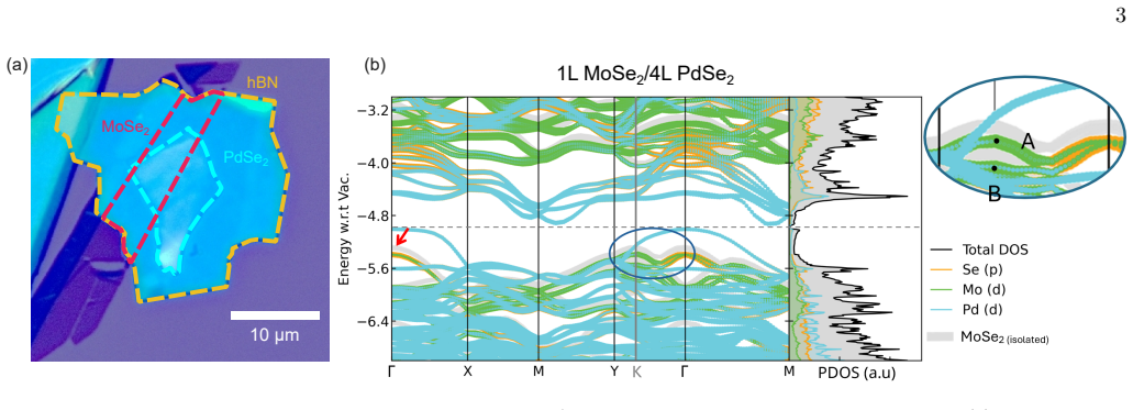
DFT band structures... hybridization... B-exciton quenching
What do these tags mean?
- matches
- The paper's claim is directly supported by a theorem in the formal canon.
- supports
- The theorem supports part of the paper's argument, but the paper may add assumptions or extra steps.
- extends
- The paper goes beyond the formal theorem; the theorem is a base layer rather than the whole result.
- uses
- The paper appears to rely on the theorem as machinery.
- contradicts
- The paper's claim conflicts with a theorem or certificate in the canon.
- unclear
- Pith found a possible connection, but the passage is too broad, indirect, or ambiguous to say the theorem truly supports the claim.
Reference graph
Works this paper leans on
-
[1]
C. Wang, F. Yang, and Y. Gao, Nanoscale Adv.2, 4323 (2020)
work page 2020
-
[2]
O. Salehzadeh, M. Djavid, N. H. Tran, I. Shih, and Z. Mi, Nano Lett.15, 5302 (2015)
work page 2015
-
[3]
I. Aharonovich, D. Englund, and M. Toth, Nat. Photonics 10, 631 (2016)
work page 2016
-
[4]
H. Kim, S. Z. Uddin, N. Higashitarumizu, E. Rabani, and A. Javey, Science373, 448 (2021)
work page 2021
-
[5]
M. A. Reshchikov, Phys. Status Solidi A218, 2000101 (2021)
work page 2021
-
[6]
D. Valerini, A. Cret´ ı, M. Lomascolo, L. Manna, R. Cin- golani, and M. Anni, Phys. Rev. B71, 235409 (2005)
work page 2005
-
[7]
Y. C. Shen, G. O. Mueller, S. Watanabe, N. F. Gardner, A. Munkholm, and M. R. Krames, Appl. Phys. Lett.91, 141101 (2007)
work page 2007
- [8]
-
[9]
J. S. Ross, P. Klement, A. M. Jones, N. J. Ghimire, J. Yan, D. G. Mandrus, T. Taniguchi, K. Watanabe, K. Kitamura, W. Yao, D. H. Cobden, and X. Xu, Nat. Nanotechnol.9, 268 (2014)
work page 2014
-
[10]
K.Lin, J.Xing, L.N.Quan, F.P.G.DeArquer, X.Gong, J. Lu, L. Xie, W. Zhao, D. Zhang, C. Yan, W. Li, X. Liu, Y. Lu, J. Kirman, E. H. Sargent, Q. Xiong, and Z. Wei, Nature562, 245 (2018)
work page 2018
-
[11]
W. Bai, T. Xuan, H. Zhao, H. Dong, X. Cheng, L. Wang, and R. Xie, Adv. Mater.35, 2302283 (2023)
work page 2023
- [12]
-
[13]
W. Zhao, R. M. Ribeiro, and G. Eda, Acc. Chem. Res. 48, 91 (2015)
work page 2015
-
[14]
A. Splendiani, L. Sun, Y. Zhang, T. Li, J. Kim, C.-Y. Chim, G. Galli, and F. Wang, Nano Lett.10, 1271 (2010)
work page 2010
-
[15]
I. Kyl¨ anp¨ a¨ a and H.-P. Komsa, Phys. Rev. B92, 205418 (2015)
work page 2015
- [16]
-
[17]
D. Xiao, G.-B. Liu, W. Feng, X. Xu, and W. Yao, Phys. Rev. Lett.108, 196802 (2012)
work page 2012
- [18]
-
[19]
C. Li, P. Zhou, and D. W. Zhang, J. Semicond.38, 031005 (2017)
work page 2017
-
[20]
A. K. Geim and I. V. Grigorieva, Nature499, 419 (2013)
work page 2013
-
[21]
A. Raja, A. Chaves, J. Yu, G. Arefe, H. M. Hill, A. F. Rigosi, T. C. Berkelbach, P. Nagler, C. Sch¨ uller, T. Korn, C. Nuckolls, J. Hone, L. E. Brus, T. F. Heinz, D. R. Reich- man, and A. Chernikov, Nat. Commun.8, 15251 (2017)
work page 2017
-
[22]
A. Chernikov, T. C. Berkelbach, H. M. Hill, A. Rigosi, Y. Li, B. Aslan, D. R. Reichman, M. S. Hybertsen, and T. F. Heinz, Phys. Rev. Lett.113, 076802 (2014)
work page 2014
-
[23]
M. Amani, D.-H. Lien, D. Kiriya, J. Xiao, A. Azcatl, J. Noh, S. R. Madhvapathy, R. Addou, S. Kc, M. Dubey, K. Cho, R. M. Wallace, S.-C. Lee, J.-H. He, J. W. Ager, X. Zhang, E. Yablonovitch, and A. Javey, Science350, 1065 (2015)
work page 2015
- [24]
- [25]
-
[26]
J. Wierzbowski, J. Klein, F. Sigger, C. Straubinger, M. Kremser, T. Taniguchi, K. Watanabe, U. Wurstbauer, A. W. Holleitner, M. Kaniber, K. M¨ uller, and J. J. Finley, Sci. Rep.7, 12383 (2017)
work page 2017
-
[27]
H. Ryu, S. C. Hong, K. Kim, Y. Jung, Y. Lee, K. Lee, Y. Kim, H. Kim, K. Watanabe, T. Taniguchi, J. Kim, K. Kim, H. Cheong, and G.-H. Lee, Nanoscale16, 5836 (2024)
work page 2024
-
[28]
Q. Li, A. Alfrey, J. Hu, N. Lydick, E. Paik, B. Liu, H. Sun, Y. Lu, R. Wang, S. Forrest, and H. Deng, Nat. Commun.14, 1837 (2023)
work page 2023
-
[29]
A. O. A. Tanoh, J. Alexander-Webber, Y. Fan, N. Gau- riot, J. Xiao, R. Pandya, Z. Li, S. Hofmann, and A. Rao, Nanoscale Adv.3, 4216 (2021)
work page 2021
-
[30]
Z. Li, H. Bretscher, Y. Zhang, G. Delport, J. Xiao, A. Lee, S. D. Stranks, and A. Rao, Nat. Commun.12, 6044 (2021)
work page 2021
-
[31]
H. Li, A. W. Contryman, X. Qian, S. M. Ardakani, Y. Gong, X. Wang, J. M. Weisse, C. H. Lee, J. Zhao, P. M. Ajayan, J. Li, H. C. Manoharan, and X. Zheng, Nat. Commun.6, 7381 (2015)
work page 2015
-
[32]
H. Lee, Y. Koo, J. Choi, S. Kumar, H.-T. Lee, G. Ji, S. H. Choi, M. Kang, K. K. Kim, H.-R. Park, H. Choo, and K.-D. Park, Sci. Adv.8, eabm5236 (2022)
work page 2022
-
[33]
H. H. Fang, B. Han, C. Robert, M. A. Semina, D. Lagarde, E. Courtade, T. Taniguchi, K. Watanabe, T. Amand, B. Urbaszek, M. M. Glazov, and X. Marie, Phys. Rev. Lett.123, 067401 (2019)
work page 2019
-
[34]
H. J. Conley, B. Wang, J. I. Ziegler, R. F. Haglund, S. T. Pantelides, and K. I. Bolotin, Nano Lett.13, 3626 (2013)
work page 2013
-
[35]
Y. Liu, N. O. Weiss, X. Duan, H.-C. Cheng, Y. Huang, and X. Duan, Nat. Rev. Mater.1, 16042 (2016)
work page 2016
-
[36]
M. Z. Bellus, M. Li, S. D. Lane, F. Ceballos, Q. Cui, 10 X. C. Zeng, and H. Zhao, Nanoscale Horiz.2, 31 (2017)
work page 2017
-
[37]
M. A. Altvater, C. E. Stevens, N. A. Pike, J. R. Hen- drickson, R. Rao, S. Krylyuk, A. V. Davydov, D. Jariwala, R. Pachter, M. Snure, and N. R. Glavin, npj 2D Mater. Appl.9, 31 (2025)
work page 2025
-
[38]
J. Duan, P. Chava, M. Ghorbani-Asl, D. Erb, L. Hu, A. V. Krasheninnikov, H. Schneider, L. Rebohle, A. Erbe, M. Helm, Y. Zeng, S. Zhou, and S. Prucnal, Adv. Funct. Mater.31, 2104960 (2021)
work page 2021
- [39]
-
[40]
M. S. Ramzan and C. Cocchi, Nanomaterials13, 2740 (2023)
work page 2023
- [41]
-
[42]
M. Long, Y. Wang, P. Wang, X. Zhou, H. Xia, C. Luo, S. Huang, G. Zhang, H. Yan, Z. Fan, X. Wu, X. Chen, W. Lu, and W. Hu, ACS Nano13, 2511 (2019)
work page 2019
-
[43]
A. Slavich, G. Ermolaev, N. Pak, D. Grudinin, K. Kravtsov, M. Tatmyshevskiy, V. Semkin, A. Syuy, A. Mazitov, A. Minnekhanov, I. Kazantsev, D. Dyubo, A. Eghbali, D. Yakubovsky, M. Kashchenko, M. Podobrii, E. Titova, A. Melentev, E. Zhukova, G. Tselikov, I. Kruglov, D. Svintsov, S. Novikov, A. Vyshnevyy, A. Ar- senin, K. S. Novoselov, and V. Volkov, Nat. Co...
work page 2025
- [44]
-
[45]
J. S. Ross, S. Wu, H. Yu, N. J. Ghimire, A. M. Jones, G. Aivazian, J. Yan, D. G. Mandrus, D. Xiao, W. Yao, and X. Xu, Nat. Commun.4, 1474 (2013)
work page 2013
-
[46]
M. M. Ugeda, A. J. Bradley, S.-F. Shi, F. H. Da Jornada, Y. Zhang, D. Y. Qiu, W. Ruan, S.-K. Mo, Z. Hussain, Z.- X. Shen, F. Wang, S. G. Louie, and M. F. Crommie, Nat. Mater.13, 1091 (2014)
work page 2014
-
[47]
G. Wang, A. Chernikov, M. M. Glazov, T. F. Heinz, X. Marie, T. Amand, and B. Urbaszek, Rev. Mod. Phys. 90, 021001 (2018)
work page 2018
- [48]
-
[49]
A. D. Oyedele, S. Yang, L. Liang, A. A. Puretzky, K. Wang, J. Zhang, P. Yu, P. R. Pudasaini, A. W. Ghosh, Z. Liu, C. M. Rouleau, B. G. Sumpter, M. F. Chisholm, W. Zhou, P. D. Rack, D. B. Geohegan, and K. Xiao, J. Am. Chem. Soc.139, 14090 (2017)
work page 2017
- [50]
-
[51]
Y. Zhang, T.-R. Chang, B. Zhou, Y.-T. Cui, H. Yan, Z. Liu, F. Schmitt, J. Lee, R. Moore, Y. Chen, H. Lin, H.-T. Jeng, S.-K. Mo, Z. Hussain, A. Bansil, and Z.-X. Shen, Nat. Nanotechnol.9, 111 (2014)
work page 2014
- [52]
-
[53]
M. Liu, L. Qi, Y. Zou, N. Zhang, F. Zhang, H. Xiang, Z. Liu, M. Qin, X. Sun, Y. Zheng, C. Lin, D. Li, and S. Li, Nat. Commun.16, 2774 (2025)
work page 2025
- [54]
-
[55]
Y. Sun, Z. Zhou, Z. Huang, J. Wu, L. Zhou, Y. Cheng, J. Liu, C. Zhu, M. Yu, P. Yu, W. Zhu, Y. Liu, J. Zhou, B. Liu, H. Xie, Y. Cao, H. Li, X. Wang, K. Liu, X. Wang, J. Wang, L. Wang, and W. Huang, Adv. Mater.31, 1806562 (2019)
work page 2019
-
[56]
T. Yamaoka, H. E. Lim, S. Koirala, X. Wang, K. Shi- nokita, M. Maruyama, S. Okada, Y. Miyauchi, and K. Matsuda, Adv. Funct. Mater.28, 1801021 (2018)
work page 2018
-
[57]
S.-T. Varjamo, C. Edwards, Y. Zhou, R. Fang, S. H. Hosseini Shokouh, and Z. Sun, Nano Lett.25, 4379 (2025)
work page 2025
-
[58]
R. H. Lone, S. Gaonkar, B. M. Kumar, and E. S. Kannan, Nanoscale17, 1473 (2025)
work page 2025
- [59]
- [60]
- [61]
- [62]
-
[63]
A. Estrada-Real, I. Paradisanos, P. R. Wiecha, J.-M. Poumirol, A. Cuche, G. Agez, D. Lagarde, X. Marie, V. Larrey, J. M¨ uller, G. Larrieu, V. Paillard, and B. Ur- baszek, Commun. Phys.6, 102 (2023)
work page 2023
-
[64]
A. Castellanos-Gomez, M. Buscema, R. Molenaar, V. Singh, L. Janssen, H. S. J. Van Der Zant, and G. A. Steele, 2D Mater.1, 011002 (2014)
work page 2014
- [65]
- [66]
- [67]
-
[68]
P. E. Bl¨ ochl, Phys. Rev. B50, 17953–17979 (1994)
work page 1994
-
[69]
J. P. Perdew, K. Burke, and M. Ernzerhof, Phys. Rev. Lett.77, 3865–3868 (1996)
work page 1996
-
[70]
M. Dion, H. Rydberg, E. Schr¨ oder, D. C. Langreth, and B. I. Lundqvist, Phys. Rev. Lett.92, 246401 (2004)
work page 2004
-
[71]
A. D. Oyedele, S. Yang, L. Liang, A. A. Puretzky, K. Wang, J. Zhang, P. Yu, P. R. Pudasaini, A. W. Ghosh, Z. Liu, C. M. Rouleau, B. G. Sumpter, M. F. Chisholm, W. Zhou, P. D. Rack, D. B. Geohegan, and K. Xiao, J. Am. Chem. Soc.139, 14090–14097 (2017)
work page 2017
-
[72]
A. Hjorth Larsen, J. Jørgen Mortensen, J. Blomqvist, I. E. Castelli, R. Christensen, M. Du lak, J. Friis, M. N. Groves, B. Hammer, C. Hargus, E. D. Hermes, P. C. Jennings, P. Bjerre Jensen, J. Kermode, J. R. Kitchin, E. Leonhard Kolsbjerg, J. Kubal, K. Kaasb- jerg, S. Lysgaard, J. Bergmann Maronsson, T. Max- son, T. Olsen, L. Pastewka, A. Peterson, C. Ros...
work page 2017
-
[73]
A. M Ganose, A. J Jackson, and D. O Scanlon, J. Open Source Softw.3, 717 (2018). 1 SUPPOR TING INFORMA TION Raman spectroscopy Figure S1 presents the Raman spectra acquired from three regions: PdSe2 on hBN, the 1L region, and the HS region. Low-frequency Raman spectroscopy (0–100 cm−1) is a widely used, non-destructive probe of interlayer vibrational mode...
work page 2018
discussion (0)
Sign in with ORCID, Apple, or X to comment. Anyone can read and Pith papers without signing in.