Depletion-mode N-polar AlN-based high electron mobility transistors with improved on/off ratios
Pith reviewed 2026-06-30 20:52 UTC · model grok-4.3
The pith
N-polar AlN HEMTs with 5.2 nm GaN channel reach on/off ratios of 10,000.
A machine-rendered reading of the paper's core claim, the machinery that carries it, and where it could break.
Core claim
Depletion-mode N-polar AlN-based HEMTs with a 5.2 nm GaN channel on N-polar AlN achieve on/off ratios as high as 10,000 through the use of an abrupt AlN/GaN heterostructure with a dedicated AlN transition layer combined with improved gate leakage control.
What carries the argument
The abrupt AlN/GaN heterostructure with a dedicated AlN transition layer that enables the high on/off ratio by reducing gate leakage.
If this is right
- The devices exhibit saturation currents exceeding 240 mA/mm at threshold voltages of -2.4 to -3.0 V.
- High frequency properties and on-resistance of about 20 Ohm mm are limited by the 2000 Ohm/square sheet resistance.
- These HEMTs offer improved switching characteristics compared to prior N-polar AlN-based devices.
Where Pith is reading between the lines
- Similar heterostructure designs could be tested in other material systems to boost on/off ratios without changing the channel material.
- Reducing the sheet resistance through better doping or mobility engineering would directly improve the on-resistance and frequency performance.
- The approach may enable better integration in power electronics where high on/off ratios are critical for efficiency.
Load-bearing premise
The measured gain in on/off ratio stems mainly from the abrupt heterostructure and AlN transition layer instead of differences in epitaxial quality, passivation, or gate processing.
What would settle it
Fabricate control devices without the AlN transition layer but with matched material quality and gate stacks, then compare their on/off ratios and gate leakage currents.
Figures
read the original abstract
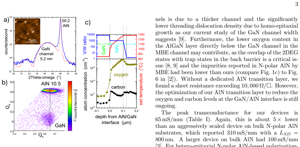
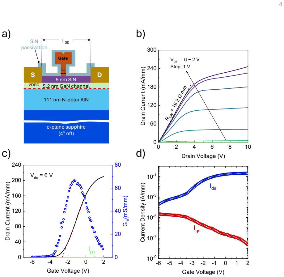
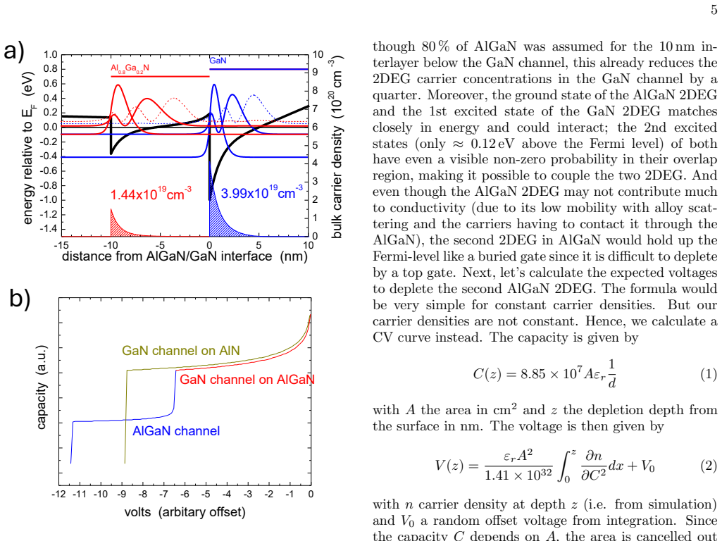
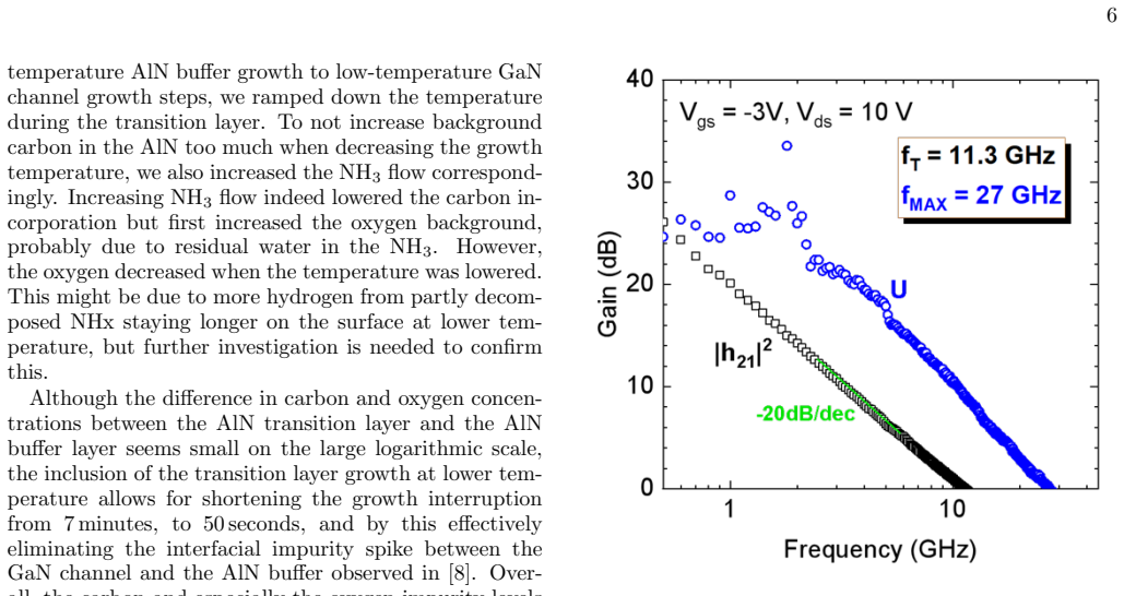
We report N-polar AlN-based high-electron mobility transistors (HEMTs) with a GaN channel thickness of 5.2 nm on N-polar AlN on sapphire. The threshold voltage is around -2.4 to -3.0 V with saturation currents over 240 mA/mm and on/off ratios as high as 10,000, much higher than previously reported N-polar AlN-based HEMTs. The high on/off ratio is attributed to the use of an abrupt AlN/GaN heterostructure with a dedicated AlN transition layer, together with improved gate leakage. The high frequency properties as well as the on-resistance of ~20 Ohm mm are all limited by the 2000 Ohm/square sheet resistance of the channel layer.
Editorial analysis
A structured set of objections, weighed in public.
Referee Report
Summary. The manuscript reports fabrication and electrical characterization of depletion-mode N-polar AlN-based HEMTs with a 5.2 nm GaN channel on N-polar AlN/sapphire. Devices show threshold voltages of -2.4 to -3.0 V, saturation currents >240 mA/mm, on/off ratios up to 10,000 (higher than prior N-polar AlN HEMTs), and on-resistance ~20 Ohm mm limited by 2000 Ohm/square sheet resistance. The high on/off ratio is attributed to an abrupt AlN/GaN heterostructure enabled by a dedicated AlN transition layer together with improved gate leakage.
Significance. If the reported metrics are reproducible, the work provides a concrete experimental demonstration of improved on/off performance in the N-polar AlN HEMT system. The explicit metrics (on/off 10,000, I_dsat >240 mA/mm) are load-bearing for the performance claim. However, the manuscript does not include the controlled comparisons or supporting measurements needed to substantiate the causal attribution to the heterostructure design.
major comments (1)
- [Abstract] Abstract (and corresponding Results/Discussion sections): The central claim attributes the on/off ratio improvement specifically to the abrupt AlN/GaN heterostructure plus dedicated AlN transition layer (plus lower gate leakage). No controlled comparison data (e.g., same-channel devices fabricated with/without the transition layer, or leakage-current vs. bias plots isolating the heterostructure contribution) are presented. This leaves open the possibility that differences in epitaxial quality, surface passivation, or gate-stack processing dominate the observed improvement.
minor comments (2)
- [Abstract] Abstract: Reported metrics lack error bars, number of devices measured, or statistical variation; direct comparison plots to prior N-polar AlN HEMTs are not referenced.
- The manuscript would benefit from explicit statements of how many devices were measured and whether the on/off values represent typical or best-case results.
Simulated Author's Rebuttal
We thank the referee for the detailed review and constructive comment. We address the major point below and agree that the causal attribution requires clarification in the text.
read point-by-point responses
-
Referee: [Abstract] Abstract (and corresponding Results/Discussion sections): The central claim attributes the on/off ratio improvement specifically to the abrupt AlN/GaN heterostructure plus dedicated AlN transition layer (plus lower gate leakage). No controlled comparison data (e.g., same-channel devices fabricated with/without the transition layer, or leakage-current vs. bias plots isolating the heterostructure contribution) are presented. This leaves open the possibility that differences in epitaxial quality, surface passivation, or gate-stack processing dominate the observed improvement.
Authors: We agree that the manuscript does not contain controlled comparison experiments (with/without the AlN transition layer on identical channel structures) or dedicated leakage plots that isolate the heterostructure contribution. The attribution in the abstract and discussion is based on the epitaxial design that enables an abrupt interface (as confirmed by the growth sequence and structural data in the manuscript) together with the measured reduction in gate leakage relative to prior N-polar AlN HEMT reports. We acknowledge that other variables cannot be excluded without additional controls. We will revise the abstract and relevant discussion paragraphs to state that the reported on/off ratio of 10,000 is achieved with the 5.2 nm GaN channel and dedicated AlN transition layer, while noting that the design is intended to promote abruptness and that direct isolation of each factor would require further experiments. This constitutes a partial revision limited to textual clarification. revision: partial
Circularity Check
No circularity: pure experimental device report with no derivations or models
full rationale
The manuscript is an experimental report of fabricated N-polar AlN HEMTs, including growth details, device processing, and measured DC and RF characteristics. No equations, fitted parameters, theoretical derivations, or predictive models are present. The attribution of on/off ratio improvement to the heterostructure is an interpretive statement, not a derivation that reduces to inputs by construction. No self-citations function as load-bearing uniqueness theorems. The paper is self-contained against external benchmarks as a materials/device fabrication study.
Axiom & Free-Parameter Ledger
axioms (1)
- domain assumption Formation of a two-dimensional electron gas at the N-polar AlN/GaN interface under the stated growth conditions
Reference graph
Works this paper leans on
-
[1]
C. Zhang, Y. Yin, P. Huang, I. Furuhashi, R. Yoann, M. Pristovsek, M. Kuball, and M. D. Smith, N-polar AlN- based enhancement-mode transistor with p-NiO x gate stacks and reduced buffer trapping, J. Phys. D: Appl. Phys. 10.1088/1361-6463/ae161c (2025)
-
[2]
Singhal, J
J. Singhal, J. Encomendero, Y. Cho, L. van Deurzen, Z. Zhang, K. Nomoto, M. Toita, H. G. Xing, and D. Jena, Molecular beam homoepitaxy of N-polar AlN on bulk AlN substrates, AIP Advances12, 095314 (2022)
2022
-
[3]
E. Kim, Z. Zhang, J. Singhal, K. Nomoto, A. Hickman, M. Toita, D. Jena, and H. G. Xing, First demonstra- tion of N-polar GaN/AlGaN/AlN HEMT on single crys- tal AlN substrates, in2022 Device Research Conference (DRC)(2022) pp. 1–2
2022
-
[4]
E. Kim, Z. Zhang, J. Encomendero, J. Singhal, K. Nomoto, A. Hickman, C. Wang, P. Fay, M. Toita, D. Jena, and H. G. Xing, N-polar GaN/AlGaN/AlN high electron mobility transistors on single-crystal bulk AlN substrates, Appl. Phys. Lett.122, 092104 (2023)
2023
-
[5]
Isono, T
T. Isono, T. Ito, R. Sakamoto, Y. Yao, Y. Ishikawa, N. Okada, and K. Tadatomo, Growth of N-polar alu- minum nitride on vicinal sapphire substrates and alu- minum nitride bulk substrates, phys. stat. solidi (b)257, 1900588 (2020)
2020
-
[6]
Miyamoto, W
M. Miyamoto, W. Matsumura, R. Okuno, S. Mat- suda, K. Hanasaku, T. Kowaki, D. Inahara, S. Kurai, N. Okada, and Y. Yamada, Improvement of electrical properties by insertion of AlGaN interlayer for N-polar AlGaN/AlN structures on sapphire substrates, Jpn. J. Appl. Phys.62, SN1016 (2023)
2023
-
[7]
Pampili and M
P. Pampili and M. Pristovsek, Nitrogen-polar growth of AlN on vicinal (0001) sapphire by MOVPE, J. Appl. Phys.135, 195303 (2024)
2024
-
[8]
M. Pristovsek, I. Furuhashi, X. Yang, C. Zhang, and M. D. Smith, Two-dimensional electron gas in thin N- polar GaN channels on AlN on sapphire templates, Crys- tals14, 10.3390/cryst14090822 (2024)
-
[9]
R. Yoann, I. Furuhashi, and M. Pristovsek, The lim- its of electrical transport in thin GaN channels on N- polar AlN, J. Semiconductorsin print, 10.1088/1674- 4926/26010034 (2026)
-
[10]
M. Hu, P. Wang, D. Wang, Y. Wu, S. Mondal, D. Wang, E. Ahmadi, T. Ma, and Z. Mi, Heteroepitaxy of n-polar aln on c-face 4h-sic: Structural and optical properties, APL Materials11, 121111 (2023)
2023
-
[11]
Namikawa, K
G. Namikawa, K. Shojiki, R. Yoshida, R. Kusuda, K. Ue- sugi, and H. Miyake, Movpe growth of aln and algan films on n-polar annealed and sputtered aln templates, J. Crys- tal Growth617, 127256 (2023)
2023
-
[12]
Y. Yang, X. Ni, Q. Fan, and X. Gu, Study of low- temperature (Al)GaN on N-Polar GaN films grown by MOCVD on vicinal SiC substrates, Materials18, 10.3390/ma18030638 (2025)
-
[13]
Kowaki, K
T. Kowaki, K. Hanasaku, M. Miyamoto, A. H. Zazuli, D. Inahara, K. Fujii, T. Kimoto, R. Ninoki, S. Kurai, N. Okada, and Y. Yamada, Effect of the twist crys- tallinity of N-polar AlN underlayer on the electrical prop- erties of GaN/AlN structures, physica status solidi (a) 221, 2400053 (2024)
2024
-
[14]
Lemettinen, H
J. Lemettinen, H. Okumura, T. Palacios, and S. Suihko- nen, N-polar AlN buffer growth by metal–organic vapor phase epitaxy for transistor applications, Appl. Phys. Ex- press11, 101002 (2018)
2018
-
[15]
Lemettinen, N
J. Lemettinen, N. Chowdhury, H. Okumura, I. Kim, S. Suihkonen, and T. Palacios, Nitrogen-polar polarization-doped field-effect transistor based on Al0.8Ga0.2N/AlN on SiC with drain current over 100 ma/mm, IEEE Electron Device Letters40, 1245 (2019)
2019
-
[16]
Inahara, S
D. Inahara, S. Matsuda, W. Matsumura, R. Okuno, K. Hanasaku, T. Kowaki, M. Miyamoto, Y. Yao, Y. Ishikawa, A. Tanaka, Y. Honda, S. Nitta, H. Amano, S. Kurai, N. Okada, and Y. Yamada, Investigation of elec- trical properties of N-polar AlGaN/AlN heterostructure field-effect transistors, phys. stat. solidi (a)220, 2200871 (2023)
2023
-
[17]
A. H. Zazuli, T. Kowaki, M. Miyamoto, K. Hanasaku, D. Inahara, K. Fujii, S. Kurai, N. Okada, and Y. Yamada, Electrical properties of N-polar GaN/AlGaN/AlN grown via metal-organic vapor phase epitaxy, physica status so- lidi (a)221, 2400060 (2024). 8
2024
-
[18]
A. H. Zazuli, T. Kowaki, M. Miyamoto, K. Hanasaku, D. Inahara, K. Fujii, T. Kimoto, R. Ninoki, S. Kurai, N. Okada, and Y. Yamada, Impact of thick N-polar AlN growth on crystalline quality and electrical properties of N-polar GaN/AlGaN/AlN FET, Jpn. J. Appl. Phys.63, 09SP11 (2024)
2024
-
[19]
Yoshikawa, T
A. Yoshikawa, T. Nagatomi, K. Nagase, S. Sugiyama, and L. J. Schowalter, Pseudomorphic growth of a thin-GaN layer on the AlN single-crystal substrate using metal or- ganic vapor phase epitaxy, Jpn. J. Appl. Phys.63, 060903 (2024)
2024
-
[20]
Y. Yang, X. Zhang, M. Qin, J. Liu, C. Zhang, Z. Hui, Y. Li, Z. Zeng, and Y. Zhang, The effect of interface po- larity on the basal dislocations at the GaN/AlN interface, Phys. Chem. Chem. Phys.27, 355 (2025)
2025
-
[21]
Singisetti, M
U. Singisetti, M. H. Wong, and U. K. Mishra, High- performance N-polar GaN enhancement-mode device technology, Semicond. Sci. Technol.28, 074006 (2013)
2013
-
[22]
E. Akso, H. Collins, K. Khan, B. Wang, W. Li, C. Clymore, E. Kayede, W. Liu, T. Chavan, R. Hamwey, N. Hatui, M. Guidry, B. Romanczyk, S. Keller, and U. K. Mishra, Schottky barrier gate N-Polar GaN-on-sapphire deep recess HEMT with record 10.5 dB linear gain and 50.2 % PAE at 94 GHz, IEEE Microwave and Wireless Technology Letters34, 183 (2024)
2024
-
[23]
Soman, M
R. Soman, M. Malakoutian, J.-k. Kim, E. Akso, N. Ha- tui, C. Wurm, U. Mishra, and S. Chowdhury, Integration of 150 nm gate length N-polar GaN MIS-HEMT devices with all-around diamond for device-level cooling, APEX 18, 046503 (2025)
2025
-
[24]
Kotani, K
J. Kotani, K. Makiyama, T. Ohki, S. Ozaki, N. Okamoto, Y. Minoura, M. Sato, N. Nakamura, and Y. Miyamoto, High-power-density InAlGaN/GaN HEMT using InGaN back barrier for W-band amplifiers, Electronics Letters 59, e12715 (2023)
2023
-
[25]
Y. Cao, T. Zimmermann, H. Xing, and D. Jena, Polarization-engineered removal of buffer leakage for GaN transistors, Applied Physics Letters96, 042102 (2010)
2010
-
[26]
D. J. Meyer, D. S. Katzer, D. A. Deen, D. F. Storm, S. C. Binari, and T. Gougousi, Hfo 2-insulated gate N- polar GaN HEMTs with high breakdown voltage, physica status solidi (a)208, 1630 (2011)
2011
discussion (0)
Sign in with ORCID, Apple, or X to comment. Anyone can read and Pith papers without signing in.