Spin-Orbit Coupling Effects on the Structural and Electronic Properties of Planar Pentagonal p-MS₂ (M = Si, Ge, and Pb)
Pith reviewed 2026-06-29 06:58 UTC · model grok-4.3
The pith
Spin-orbit coupling turns p-PbS2 from metal into semiconductor with a 0.475 eV quasi-direct gap.
A machine-rendered reading of the paper's core claim, the machinery that carries it, and where it could break.
Core claim
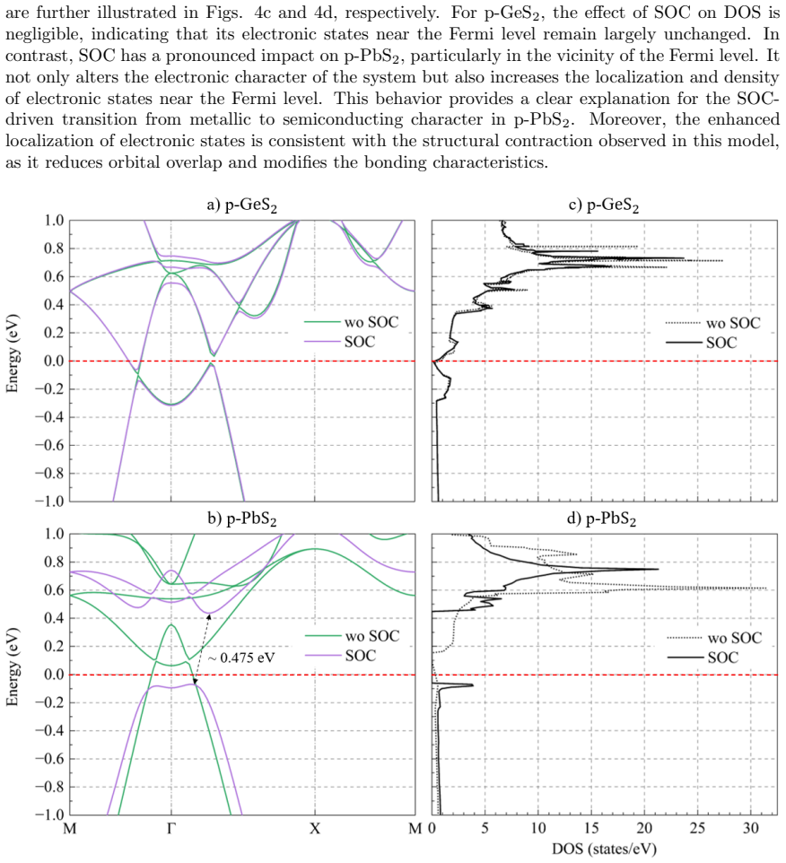
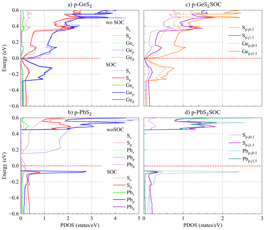
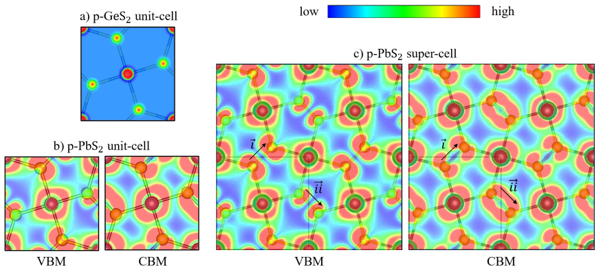
SOC enhances electronic localization, producing a slight structural contraction and a reconstruction of electronic states near the Fermi level that becomes stronger for heavier M atoms. While p-GeS2 remains metallic, SOC drives a metal-semiconductor transition in p-PbS2 and opens a quasi-direct band gap of about 0.475 eV, with the conduction band minimum state exhibiting pronounced anisotropy along the S-S bonds.
What carries the argument
Spin-orbit coupling included in DFT calculations on the planar pentagonal lattice, which increases localization and shifts bands near the Fermi energy.
If this is right
- p-PbS2 acquires a quasi-direct gap of 0.475 eV once SOC is included.
- The conduction-band minimum in p-PbS2 becomes strongly anisotropic along S-S bonds.
- p-GeS2 stays metallic even after SOC is turned on.
- The magnitude of the structural contraction and band reconstruction increases with heavier central atoms.
- p-PbS2 is identified as a candidate for gas-sensing devices due to the anisotropic conduction state.
Where Pith is reading between the lines
- The same SOC-driven localization may appear in other planar or buckled chalcogenide sheets that contain heavy atoms.
- Direction-dependent transport or adsorption properties could be tested if single-layer p-PbS2 can be isolated.
- Hybrid-functional or GW calculations would provide an independent check on the 0.475 eV gap value.
- Experimental synthesis attempts could first target whether the pentagonal phase of PbS2 can be stabilized at all.
Load-bearing premise
The planar pentagonal geometry stays the relevant structure after SOC is added and standard DFT functionals give the correct relative stability and gap size.
What would settle it
An experimental band-structure measurement on p-PbS2 that shows no gap opening or a metallic state after SOC is accounted for would disprove the transition.
Figures
read the original abstract
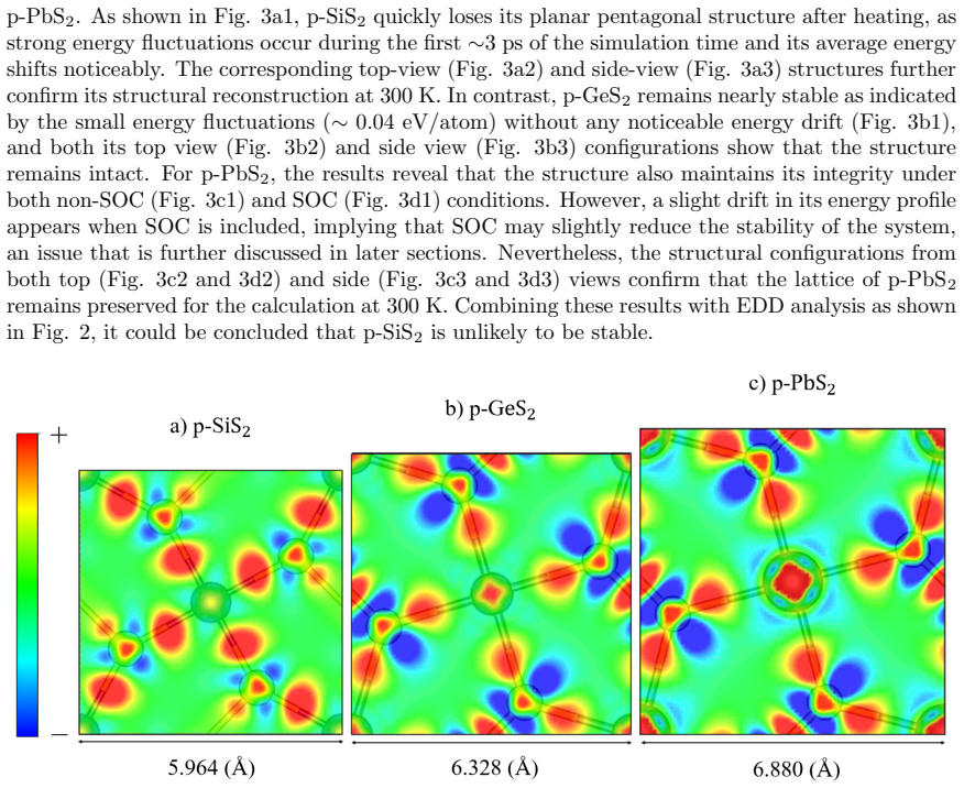
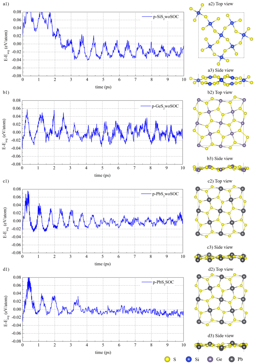
Spin-orbit coupling (SOC) plays an important role in determining the structural and electronic properties of recently proposed two-dimensional planar pentagonal materials. In this work, density functional theory calculations are employed to investigate SOC effects in p-MS$_{2}$ systems (M = Si, Ge, and Pb). Our results indicate that the p-SiS$_{2}$ structure is likely unstable, except for p-GeS$_{2}$ and p-PbS$_{2}$. A detailed j-resolved (total angular momentum) orbital analysis reveals that SOC enhances electronic localization, leading to a slight structural contraction and a reconstruction of electronic states near the Fermi level, this effect becoming stronger for heavier M atoms. While p-GeS$_{2}$ remains metallic, SOC drives a metal-semiconductor transition in p-PbS$_{2}$ and opening a quasi-direct band gap of about 0.475 eV. In addition, the conduction band minimum state of p-PbS$_{2}$ exhibits pronounced anisotropy along the S-S bonds. These findings provide insight into SOC-driven structural and electronic reconstruction in planar pentagonal chalcogenides p-MS$_{2}$ and suggest that p-PbS$_{2}$ may be a promising candidate for gas-sensing applications.
Editorial analysis
A structured set of objections, weighed in public.
Referee Report
Summary. The paper employs density functional theory to examine spin-orbit coupling (SOC) effects on the structural and electronic properties of planar pentagonal p-MS₂ (M = Si, Ge, Pb). It reports that p-SiS₂ is likely unstable, p-GeS₂ remains metallic, while SOC induces a metal-semiconductor transition in p-PbS₂, opening a quasi-direct gap of ~0.475 eV with anisotropic conduction band minimum states along S-S bonds; SOC is said to enhance localization and cause slight contraction, with stronger effects for heavier M.
Significance. If robust, the work would illustrate how SOC can drive electronic reconstruction and a gap opening in heavier pentagonal chalcogenides, identifying p-PbS₂ as potentially relevant for sensing applications. The j-resolved orbital analysis provides some mechanistic insight, but the absence of any reported convergence tests, functional benchmarks, or stability checks limits the assessed significance.
major comments (2)
- [Abstract] Abstract: The central claim of an SOC-driven metal-semiconductor transition and 0.475 eV quasi-direct gap in p-PbS₂ rests on unverified DFT+SOC results; no functional (e.g., PBE), k-point sampling, or convergence data are mentioned, leaving open the possibility that the gap is an artifact of GGA underestimation near the metal-insulator boundary.
- [Abstract] Abstract: The assumption that the planar pentagonal geometry remains the ground state after SOC inclusion is load-bearing for all reported structural and electronic changes, yet no phonon dispersion, total-energy comparisons, or hybrid-functional checks with SOC are referenced to confirm stability.
minor comments (2)
- [Abstract] Abstract: The phrase 'about 0.475 eV' should be replaced by a precise value with uncertainty or the exact computed number for reproducibility.
- [Abstract] Abstract: 'j-resolved (total angular momentum) orbital analysis' is introduced without defining the projection method or basis used, which would aid clarity.
Simulated Author's Rebuttal
We thank the referee for the constructive comments, which help strengthen the presentation of our DFT results on SOC effects in planar pentagonal p-MS₂ systems. We will revise the manuscript to incorporate explicit computational details, convergence information, and additional stability analyses as outlined below.
read point-by-point responses
-
Referee: [Abstract] Abstract: The central claim of an SOC-driven metal-semiconductor transition and 0.475 eV quasi-direct gap in p-PbS₂ rests on unverified DFT+SOC results; no functional (e.g., PBE), k-point sampling, or convergence data are mentioned, leaving open the possibility that the gap is an artifact of GGA underestimation near the metal-insulator boundary.
Authors: The manuscript employs the PBE functional with SOC as standard for these systems, with k-point sampling and cutoff parameters detailed in the Methods section. We acknowledge that these are not summarized in the abstract. In revision we will add a brief statement of the functional, sampling, and convergence criteria to the abstract and include explicit convergence tests (energy cutoff, k-mesh density) plus a short hybrid-functional benchmark (HSE06+SOC) on the PbS₂ gap to rule out GGA artifacts near the transition. revision: yes
-
Referee: [Abstract] Abstract: The assumption that the planar pentagonal geometry remains the ground state after SOC inclusion is load-bearing for all reported structural and electronic changes, yet no phonon dispersion, total-energy comparisons, or hybrid-functional checks with SOC are referenced to confirm stability.
Authors: Structural optimizations were performed self-consistently with SOC, and the planar pentagonal motif was preserved for GeS₂ and PbS₂. We did not report phonon dispersions or hybrid-functional total-energy comparisons with SOC. In the revised manuscript we will add phonon dispersion calculations (with SOC) for the stable compounds and, where computationally tractable, a comparison of total energies with and without SOC using a hybrid functional to further substantiate dynamical and energetic stability. revision: yes
Circularity Check
No circularity: standard DFT+SOC outputs are direct computations
full rationale
The paper reports direct results from density functional theory calculations on p-MS2 structures with and without SOC. The metal-semiconductor transition, 0.475 eV gap, and CBM anisotropy in p-PbS2 are numerical outputs of the chosen functional and SOC inclusion, not obtained by fitting parameters to the target quantities or by any self-referential definition. No equations, ansatzes, or citations reduce the central claims to their own inputs by construction. The workflow contains no self-citation load-bearing steps or uniqueness theorems imported from prior author work.
Axiom & Free-Parameter Ledger
Reference graph
Works this paper leans on
-
[1]
Electronic structure of a quasi-freestanding mos2 monolayer
T Eknapakul, PDC King, M Asakawa, P Buaphet, R-H He, S-K Mo, H Takagi, KM Shen, F Baumberger, T Sasagawa, et al. Electronic structure of a quasi-freestanding mos2 monolayer. Nano letters, 14(3):1312–1316, 2014
2014
-
[2]
Creation and control of a two-dimensional electron liquid at the bare srtio3 surface.Nature materials, 10(2):114–118, 2011
Worawat Meevasana, PDC King, RH He, SK Mo, M Hashimoto, Anna Tamai, P Songsiririt- thigul, F´ elix Baumberger, and ZX Shen. Creation and control of a two-dimensional electron liquid at the bare srtio3 surface.Nature materials, 10(2):114–118, 2011
2011
-
[3]
Hierarchy of multiple many-body interaction scales in high-temperature 12 superconductors.Physical Review B—Condensed Matter and Materials Physics, 75(17):174506, 2007
W Meevasana, XJ Zhou, S Sahrakorpi, WS Lee, WL Yang, K Tanaka, N Mannella, T Yoshida, DH Lu, YL Chen, et al. Hierarchy of multiple many-body interaction scales in high-temperature 12 superconductors.Physical Review B—Condensed Matter and Materials Physics, 75(17):174506, 2007
2007
-
[4]
Monochromatic electron photoemission from diamondoid monolayers.Science, 316(5830):1460–1462, 2007
Wanli L Yang, JD Fabbri, TM Willey, JRI Lee, JE Dahl, RMK Carlson, PR Schreiner, AA Fokin, BA Tkachenko, NA Fokina, et al. Monochromatic electron photoemission from diamondoid monolayers.Science, 316(5830):1460–1462, 2007
2007
-
[5]
Tran Yen Mi, Huynh My Linh, Trung-Phuc Vo, and Huynh Anh Huy. Sensing capabilities of the sawtooth penta-sic 2 nanoribbon for co 2 and co molecules based on variations in molecular density: insights from a dft investigation.RSC advances, 15(26):21183–21189, 2025
2025
-
[6]
Tran Yen Mi, Huynh Anh Huy, and Nguyen Thanh Tien. A comparison study of the structural, electronic and electronic transport properties of nanoribbons based on penta-graphene, penta- p2c and penta-sic2.Materials Today Communications, 32:103912, 2022
2022
-
[7]
Diverse structural and electronic properties of pentagonal sic2 nanoribbons: A first-principles study.Materials Today Communications, 26:102047, 2021
Tran Yen Mi, Nguyen Duy Khanh, Rajeev Ahuja, and Nguyen Thanh Tien. Diverse structural and electronic properties of pentagonal sic2 nanoribbons: A first-principles study.Materials Today Communications, 26:102047, 2021
2021
-
[8]
Adsorption of gas molecules on penta-graphene nanoribbon and its implication for nanoscale gas sensor.Physics Open, 2: 100014, 2020
Tran Yen Mi, Dang Minh Triet, and Nguyen Thanh Tien. Adsorption of gas molecules on penta-graphene nanoribbon and its implication for nanoscale gas sensor.Physics Open, 2: 100014, 2020
2020
-
[9]
Vo Trung Phuc, Pham Thi Bich Thao, Rajeev Ahuja, and Nguyen Thanh Tien. Effect of phosphorus doping positions on electronic transport properties in the sawtooth penta-graphene nanoribbon: first-principles insights.Solid State Communications, 353:114859, 2022
2022
-
[10]
Electronic and transport features of sawtooth penta-graphene nanoribbons via substitutional doping.Physica E: Low-dimensional Systems and Nanostructures, 114:113572, 2019
Nguyen Thanh Tien, Pham Thi Bich Thao, Vo Trung Phuc, and Rajeev Ahuja. Electronic and transport features of sawtooth penta-graphene nanoribbons via substitutional doping.Physica E: Low-dimensional Systems and Nanostructures, 114:113572, 2019
2019
-
[11]
Influence of edge termination on the electronic and transport properties of sawtooth penta-graphene nanoribbons.Journal of physics and chemistry of solids, 146:109528, 2020
Nguyen Thanh Tien, Pham Thi Bich Thao, Vo Trung Phuc, and Rajeev Ahuja. Influence of edge termination on the electronic and transport properties of sawtooth penta-graphene nanoribbons.Journal of physics and chemistry of solids, 146:109528, 2020
2020
-
[12]
Realization of an ideal cairo tessellation in nickel diazenide nin2: high-pressure route to pentagonal 2d materials.ACS nano, 15(8):13539–13546, 2021
Maxim Bykov, Elena Bykova, Alena V Ponomareva, Ferenc Tasnadi, Stella Chariton, Vitali B Prakapenka, Konstantin Glazyrin, Jesse S Smith, Mohammad F Mahmood, Igor A Abrikosov, et al. Realization of an ideal cairo tessellation in nickel diazenide nin2: high-pressure route to pentagonal 2d materials.ACS nano, 15(8):13539–13546, 2021
2021
-
[13]
The 2d materials roadmap.2D Materials, 2025
Wencai Ren, Peter Boggild, Joan M Redwing, Konstantin S Novoselov, Luzhao Sun, Yue Qi, Kaicheng Jia, Zhongfan Liu, Oliver Burton, Jack Allen Alexander-Webber, et al. The 2d materials roadmap.2D Materials, 2025
2025
-
[14]
Spectroscopic signature of negative electronic compressibility from the ti core-level of titanium carbonitride mxene.Applied Physics Reviews, 8(2), 2021
Warakorn Jindata, Kanit Hantanasirisakul, Tanachat Eknapakul, Jonathan D Denlinger, Sup- panut Sangphet, Sujinda Chaiyachad, Chutchawan Jaisuk, Aissara Rasritat, Tanawat Sawasdee, Hideki Nakajima, et al. Spectroscopic signature of negative electronic compressibility from the ti core-level of titanium carbonitride mxene.Applied Physics Reviews, 8(2), 2021
2021
-
[15]
Advanced synthesis and unique properties of 2d transition metal dichalcogenides for realizing next- generation applications.ACS Materials Au, 5(5):745–766, 2025
Chandan Patra, Subrata Mondal, Rupam Mukherjee, and Yerumbu Nandakishora. Advanced synthesis and unique properties of 2d transition metal dichalcogenides for realizing next- generation applications.ACS Materials Au, 5(5):745–766, 2025
2025
-
[16]
Mechanical exfoliation of large area 2d materials from vdw crystals.Progress in Surface Science, 96(2):100626, 2021
Fang Liu. Mechanical exfoliation of large area 2d materials from vdw crystals.Progress in Surface Science, 96(2):100626, 2021. 13
2021
-
[17]
Ruijie Yang, Liang Mei, Qingyong Zhang, Yingying Fan, Hyeon Suk Shin, Damien Voiry, and Zhiyuan Zeng. High-yield production of mono-or few-layer transition metal dichalcogenide nanosheets by an electrochemical lithium ion intercalation-based exfoliation method.Nature protocols, 17(2):358–377, 2022
2022
-
[18]
Wannier based analysis of the direct-indirect bandgap transition by stacking MoS$_2$ layers
Shunsuke Hirai, Ibuki Terada, and Michi-To Suzuki. Wannier based analysis of the direct- indirect bandgap transition by stacking mos 2 layers.arXiv preprint arXiv:2511.15178, 2025
work page internal anchor Pith review Pith/arXiv arXiv 2025
-
[19]
Recent progress in the synthesis and engineering of high-performance mos2 electrocatalysts for the hydrogen evolution reaction
Xinyue Du, Yuqing Xu, Aixian Shan, and Rongming Wang. Recent progress in the synthesis and engineering of high-performance mos2 electrocatalysts for the hydrogen evolution reaction. Catalysts, 15(7):626, 2025
2025
-
[20]
Epitaxial synthesis of monolayer ptse2 single crystal on mose2 with strong interlayer coupling.ACS nano, 13(10):10929–10938, 2019
Jiadong Zhou, Xianghua Kong, M Chandra Sekhar, Junhao Lin, Frederic Le Goualher, Rui Xu, Xiaowei Wang, Yu Chen, Yao Zhou, Chao Zhu, et al. Epitaxial synthesis of monolayer ptse2 single crystal on mose2 with strong interlayer coupling.ACS nano, 13(10):10929–10938, 2019
2019
-
[21]
Two-dimensional pentagonal materials with parabolic dispersion and high carrier mobility.Materials, 17(22):5543, 2024
Xiaofei Shao, Xiaobiao Liu, and Xikui Ma. Two-dimensional pentagonal materials with parabolic dispersion and high carrier mobility.Materials, 17(22):5543, 2024
2024
-
[22]
From node-line semimetals to large-gap quantum spin hall states in a family of pentagonal group-iva chalcogenide.Physical Review B, 97(12):125312, 2018
Run-Wu Zhang, Cheng-Cheng Liu, Da-Shuai Ma, and Yugui Yao. From node-line semimetals to large-gap quantum spin hall states in a family of pentagonal group-iva chalcogenide.Physical Review B, 97(12):125312, 2018
2018
-
[23]
Fully unconstrained noncollinear magnetism within the projector augmented-wave method.Physical Review B, 62(17):11556, 2000
D Hobbs, G Kresse, and J Hafner. Fully unconstrained noncollinear magnetism within the projector augmented-wave method.Physical Review B, 62(17):11556, 2000
2000
-
[24]
Quantum spin hall effect in magnetic graphene.Nature Communications, 16(1):5336, 2025
Talieh S Ghiasi, Davit Petrosyan, Josep Ingla-Ayn´ es, Tristan Bras, Kenji Watanabe, Takashi Taniguchi, Samuel Ma˜ nas-Valero, Eugenio Coronado, Klaus Zollner, Jaroslav Fabian, et al. Quantum spin hall effect in magnetic graphene.Nature Communications, 16(1):5336, 2025
2025
-
[25]
Spin-orbit coupling in elemental two-dimensional materials.Physical Review B, 100(12):125422, 2019
Marcin Kurpas, Paulo E Faria Junior, Martin Gmitra, and Jaroslav Fabian. Spin-orbit coupling in elemental two-dimensional materials.Physical Review B, 100(12):125422, 2019
2019
-
[26]
Two-dimensional square lattice polonium stabilized by the spin–orbit coupling
Shota Ono. Two-dimensional square lattice polonium stabilized by the spin–orbit coupling. Scientific Reports, 10(1):11810, 2020
2020
-
[27]
Spin–orbit coupling in 2d semiconductors: A theoretical perspective.The Journal of Physical Chemistry Letters, 12(51):12256–12268, 2021
Jiajia Chen, Kai Wu, Wei Hu, and Jinlong Yang. Spin–orbit coupling in 2d semiconductors: A theoretical perspective.The Journal of Physical Chemistry Letters, 12(51):12256–12268, 2021
2021
-
[28]
First-principles determi- nation of spin–orbit coupling parameters in two-dimensional materials.Nature Reviews Physics, 7(5):255–269, 2025
Klaus Zollner, Marcin Kurpas, Martin Gmitra, and Jaroslav Fabian. First-principles determi- nation of spin–orbit coupling parameters in two-dimensional materials.Nature Reviews Physics, 7(5):255–269, 2025
2025
-
[29]
Oxford University Press, 2014
Feliciano Giustino.Materials modelling using density functional theory: properties and predic- tions. Oxford University Press, 2014
2014
-
[30]
Quantum espresso: a modular and open-source software project for quantum simulations of materials
Paolo Giannozzi, Stefano Baroni, Nicola Bonini, Matteo Calandra, Roberto Car, Carlo Cavaz- zoni, Davide Ceresoli, Guido L Chiarotti, Matteo Cococcioni, Ismaila Dabo, et al. Quantum espresso: a modular and open-source software project for quantum simulations of materials. Journal of physics: Condensed matter, 21(39):395502, 2009
2009
-
[31]
Advanced capabilities for materials modelling with quantum espresso.Journal of physics: Con- densed matter, 29(46):465901, 2017
Paolo Giannozzi, Oliviero Andreussi, Thomas Brumme, Oana Bunau, M Buongiorno Nardelli, Matteo Calandra, Roberto Car, Carlo Cavazzoni, Davide Ceresoli, Matteo Cococcioni, et al. Advanced capabilities for materials modelling with quantum espresso.Journal of physics: Con- densed matter, 29(46):465901, 2017. 14
2017
-
[32]
Quantum espresso toward the exascale.The Journal of chemical physics, 152(15), 2020
Paolo Giannozzi, Oscar Baseggio, Pietro Bonf` a, Davide Brunato, Roberto Car, Ivan Carnimeo, Carlo Cavazzoni, Stefano De Gironcoli, Pietro Delugas, Fabrizio Ferrari Ruffino, et al. Quantum espresso toward the exascale.The Journal of chemical physics, 152(15), 2020
2020
-
[33]
Precision and efficiency in solid-state pseudopotential calculations.npj Computational Materi- als, 4(1):72, 2018
Gianluca Prandini, Antimo Marrazzo, Ivano E Castelli, Nicolas Mounet, and Nicola Marzari. Precision and efficiency in solid-state pseudopotential calculations.npj Computational Materi- als, 4(1):72, 2018
2018
-
[34]
Pseudopotentials periodic table: From h to pu.Computational Materials Science, 95:337–350, 2014
Andrea Dal Corso. Pseudopotentials periodic table: From h to pu.Computational Materials Science, 95:337–350, 2014
2014
-
[35]
E Kucukbenli, M Monni, BI Adetunji, X Ge, GA Adebayo, N Marzari, S De Gironcoli, and A Dal Corso. Projector augmented-wave and all-electron calculations across the periodic table: a comparison of structural and energetic properties.arXiv preprint arXiv:1404.3015, 2014
work page internal anchor Pith review Pith/arXiv arXiv 2014
-
[36]
Pseudopotentials for high-throughput dft calculations.Computational Materials Science, 81:446–452, 2014
Kevin F Garrity, Joseph W Bennett, Karin M Rabe, and David Vanderbilt. Pseudopotentials for high-throughput dft calculations.Computational Materials Science, 81:446–452, 2014
2014
-
[37]
Vesta: a three-dimensional visualization system for electronic and structural analysis.Applied Crystallography, 41(3):653–658, 2008
Koichi Momma and Fujio Izumi. Vesta: a three-dimensional visualization system for electronic and structural analysis.Applied Crystallography, 41(3):653–658, 2008
2008
-
[38]
Noah Felis and Wilke Dononelli. Falcon: fast active learning for machine learning potentials in atomistic and ab initio molecular dynamics simulations.npj Computational Materials, 12 (1):1, 2026. doi: 10.1038/s41524-025-01897-8. URLhttps://www.nature.com/articles/ s41524-025-01897-8
-
[39]
Bilbao crystallographic server: I
Mois Ilia Aroyo, Juan Manuel Perez-Mato, Cesar Capillas, Eli Kroumova, Svetoslav Ivantchev, Gotzon Madariaga, Asen Kirov, and Hans Wondratschek. Bilbao crystallographic server: I. databases and crystallographic computing programs.Zeitschrift f¨ ur Kristallographie-Crystalline Materials, 221(1):15–27, 2006
2006
-
[40]
Bilbao crystallographic server
Mois I Aroyo, Asen Kirov, Cesar Capillas, JM Perez-Mato, and Hans Wondratschek. Bilbao crystallographic server. ii. representations of crystallographic point groups and space groups. Foundations of Crystallography, 62(2):115–128, 2006
2006
-
[41]
Crystallography online: Bilbao crystallographic server.Bulg
Mois I Aroyo, Juan Manuel Perez-Mato, Danel Orobengoa, EMRE Tasci, Gemma de la Flor, and Asel Kirov. Crystallography online: Bilbao crystallographic server.Bulg. Chem. Commun, 43(2):115–128, 2011
2011
-
[42]
Single-layer planar penta-x2n4 (x= ni, pd and pt) as direct-bandgap semiconductors from first principle calculations.Applied Surface Science, 469:456–462, 2019
Jun-Hui Yuan, Ya-Qian Song, Qi Chen, Kan-Hao Xue, and Xiang-Shui Miao. Single-layer planar penta-x2n4 (x= ni, pd and pt) as direct-bandgap semiconductors from first principle calculations.Applied Surface Science, 469:456–462, 2019
2019
-
[43]
Structural defects in graphene
Florian Banhart, Jani Kotakoski, and Arkady V Krasheninnikov. Structural defects in graphene. ACS nano, 5(1):26–41, 2011
2011
-
[44]
Structures, mobilities, electronic and magnetic properties of point defects in silicene.Nanoscale, 5(20): 9785–9792, 2013
Junfeng Gao, Junfeng Zhang, Hongsheng Liu, Qinfang Zhang, and Jijun Zhao. Structures, mobilities, electronic and magnetic properties of point defects in silicene.Nanoscale, 5(20): 9785–9792, 2013
2013
-
[45]
Defects in phosphorene.The Journal of Physical Chemistry C, 119 (35):20474–20480, 2015
Wei Hu and Jinlong Yang. Defects in phosphorene.The Journal of Physical Chemistry C, 119 (35):20474–20480, 2015
2015
-
[46]
Influence of spin-orbit coupling on chemical bonding.arXiv preprint arXiv:2204.02751, 2022
Andris Gulans and Claudia Draxl. Influence of spin-orbit coupling on chemical bonding.arXiv preprint arXiv:2204.02751, 2022. 15
-
[47]
Penta-graphene: A new carbon allotrope.Proceedings of the National Academy of Sci- ences, 112(8):2372–2377, 2015
Shunhong Zhang, Jian Zhou, Qian Wang, Xiaoshuang Chen, Yoshiyuki Kawazoe, and Puru Jena. Penta-graphene: A new carbon allotrope.Proceedings of the National Academy of Sci- ences, 112(8):2372–2377, 2015
2015
-
[48]
Novel Two-dimensional SiC2 Sheet with Full Pentagon Network
J Liu, CY He, N Jiao, HP Xiao, KW Zhang, RZ Wang, and LZ Sun. Novel two-dimensional sic2 sheet with full pentagon network.arXiv preprint arXiv:1307.6324, 2013. 16
work page internal anchor Pith review Pith/arXiv arXiv 2013
discussion (0)
Sign in with ORCID, Apple, or X to comment. Anyone can read and Pith papers without signing in.