Interface Symmetry and Electrostatic Stabilization of Strain-Resilient Janus Heterobilayers for Flexible Piezotronics
Pith reviewed 2026-06-28 13:56 UTC · model grok-4.3
The pith
Electrostatic effects at the interface of MoSSe/WSSe Janus heterobilayers suppress the strain-induced band-gap transitions seen in standard TMDs.
A machine-rendered reading of the paper's core claim, the machinery that carries it, and where it could break.
Core claim
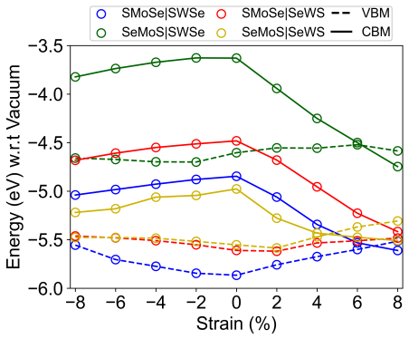
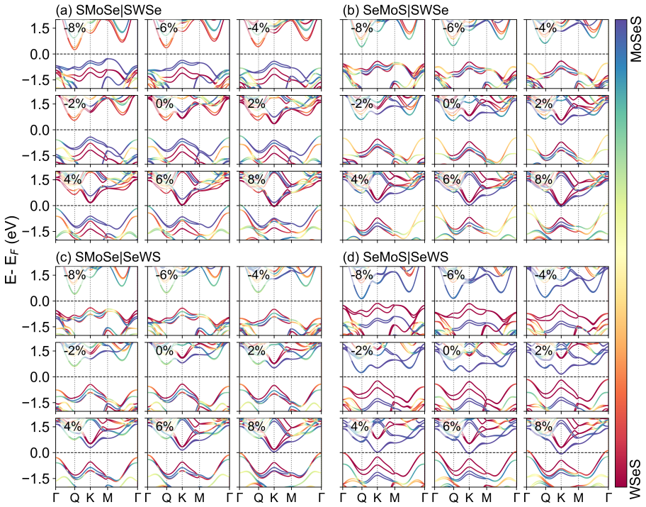
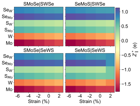
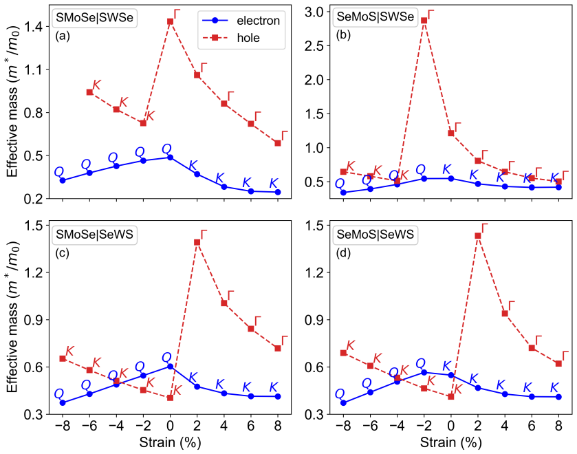
By examining different stacking configurations of MoSSe/WSSe heterobilayers, the authors show that interface chemistry modulates interlayer coupling, charge redistribution, and dipole interactions; the combined intrinsic electric fields and interface electrostatics thereby suppress strain-induced band-gap transitions typical of conventional TMDs, while the shear piezoelectric coefficient can be tuned by strain through changes in interfacial symmetry.
What carries the argument
Interface chemistry that modulates interlayer coupling, dynamic charge redistribution, and dipole interactions across different stacking configurations of the Janus heterobilayer.
If this is right
- The electronic structure remains stable against lattice deformation, enabling flexible nanoelectronic applications.
- In-plane piezoelectric response is insensitive to stacking order.
- Shear piezoelectric coefficient depends on interfacial symmetry and can be adjusted by applied strain.
- Interface engineering offers a route to strain-resilient Janus heterostructures for optoelectronic, valleytronic, and piezotronic devices.
Where Pith is reading between the lines
- The same electrostatic stabilization mechanism could apply to other Janus TMD pairs if their intrinsic dipoles produce comparable interface fields.
- Targeted growth of specific stacking orders might allow experimental tuning of the shear piezoelectric response beyond what uniform films achieve.
- These heterobilayers could widen the usable strain window for 2D piezotronic sensors compared with standard TMD monolayers.
Load-bearing premise
That the limited set of stacking configurations examined captures the dominant interface chemistry and electrostatics that would occur in real fabricated heterobilayers.
What would settle it
Observation of an indirect-to-direct band-gap transition under tensile or compressive strain in a fabricated MoSSe/WSSe heterobilayer would contradict the claimed suppression.
Figures
read the original abstract
The electronic structure of conventional two-dimensional transition metal dichalcogenides (TMDs) is highly sensitive to lattice deformation, often leading to indirect-to-direct band-gap transitions that compromise performance in flexible nanoelectronic applications. Janus TMDs, with their broken mirror symmetry and intrinsic out-of-plane dipoles, offer a promising alternative platform for electrostatic tuning. However, their electronic stability under strain and the role of the chalcogen stacking sequence in their heterostructures remains poorly understood. Here, we study from first principles the strain tolerance and piezoelectric properties of MoSSe/WSSe heterobilayers. By examining different configurations, we demonstrate that the interface chemistry strongly modulates interlayer coupling, dynamic charge redistribution, and dipole interactions. Importantly, the combined effects of intrinsic electric fields and interface electrostatics effectively suppress the strain-induced band-gap transitions typical of conventional TMDs. Moreover, while the in-plane piezoelectric response remains nearly insensitive to the stacking order, the shear piezoelectric coefficient depends heavily on the interfacial symmetry and can be effectively tuned by strain modulation. Our results highlight interfacial engineering as a powerful route to design strain-resilient Janus heterostructures for next-generation flexible optoelectronic, valleytronic, and piezotronic devices.
Editorial analysis
A structured set of objections, weighed in public.
Referee Report
Summary. The manuscript presents first-principles calculations on MoSSe/WSSe Janus heterobilayers. It claims that interface chemistry in different stacking configurations modulates interlayer coupling, charge redistribution, and dipole interactions such that the combined intrinsic electric fields and interface electrostatics suppress the strain-induced band-gap transitions typical of conventional TMDs; the in-plane piezoelectric response is nearly stacking-insensitive while the shear coefficient depends on interfacial symmetry and can be tuned by strain.
Significance. If the reported suppression is robust, the work would be significant for flexible piezotronics by identifying interfacial electrostatics as a design handle for strain-resilient Janus heterostructures.
major comments (2)
- [Abstract] Abstract: the central claim that interface electrostatics 'effectively suppress the strain-induced band-gap transitions' rests on 'examining different configurations,' yet no enumeration of high-symmetry registries, convergence with respect to stacking, or comparison to disordered interfaces is described; if other alignments yield weaker suppression, the attribution to interface chemistry is not general.
- [Abstract] Abstract/Methods (implied): no DFT functional, plane-wave cutoff, k-point mesh, strain-application protocol, or validation against known TMD strain response is stated, so the numerical support for the suppression cannot be assessed.
minor comments (1)
- [Abstract] Abstract: the phrase 'Janus heterobilayers' is used without immediate clarification that the specific MoSSe/WSSe pair is under study.
Simulated Author's Rebuttal
We thank the referee for the constructive comments on our manuscript. We address each point below and will revise the manuscript to enhance clarity and provide the requested details.
read point-by-point responses
-
Referee: [Abstract] Abstract: the central claim that interface electrostatics 'effectively suppress the strain-induced band-gap transitions' rests on 'examining different configurations,' yet no enumeration of high-symmetry registries, convergence with respect to stacking, or comparison to disordered interfaces is described; if other alignments yield weaker suppression, the attribution to interface chemistry is not general.
Authors: We agree the abstract is concise and does not enumerate the registries. The main text examines the principal high-symmetry stacking configurations (AA, AB1, AB2) that preserve the Janus character and lattice commensurability; the suppression of indirect-to-direct transitions is robust across these. To address the concern directly, we will add an explicit table or figure listing the registries, their relative formation energies, and the band-gap evolution under strain for each. Disordered interfaces lie outside the scope of this study of commensurate heterobilayers, but we will add a sentence clarifying this limitation and noting that the electrostatic stabilization mechanism is tied to the periodic interface dipole alignment present in the ordered cases. revision: yes
-
Referee: [Abstract] Abstract/Methods (implied): no DFT functional, plane-wave cutoff, k-point mesh, strain-application protocol, or validation against known TMD strain response is stated, so the numerical support for the suppression cannot be assessed.
Authors: The Methods section of the manuscript specifies the PBE+D3 functional, 500 eV plane-wave cutoff, 9 imes9 imes1 imes 1 k-mesh, and the strain protocol (uniaxial scaling of the in-plane lattice vectors with full ionic relaxation). Validation against literature monolayer TMD strain responses is also included. However, these details are not summarized in the abstract. We will add a concise methods paragraph immediately after the abstract and ensure the abstract itself references the computational framework, thereby allowing readers to assess the numerical support without ambiguity. revision: yes
Circularity Check
No significant circularity; derivation self-contained
full rationale
The paper reports first-principles calculations on MoSSe/WSSe heterobilayers, presenting the suppression of strain-induced band-gap transitions as a computed outcome from examining stacking configurations and interface electrostatics. No equations, parameters, or claims reduce by construction to fitted inputs, self-definitions, or self-citation chains. The central result is framed as an independent finding from standard DFT methods rather than a renaming or ansatz smuggled via prior work. This is the normal case of a self-contained computational study.
Axiom & Free-Parameter Ledger
Reference graph
Works this paper leans on
-
[1]
A.; Münzenrieder, N.; Barraud, C.; Petti, L.; Zysset, C.; Büthe, L.; Ensslin, K.; Tröster, G
(1) Salvatore, G. A.; Münzenrieder, N.; Barraud, C.; Petti, L.; Zysset, C.; Büthe, L.; Ensslin, K.; Tröster, G. Fabrication and Transfer of Flexible Few-Layers MoS2 Thin Film Transistors to Any Arbitrary Substrate.ACS Nano2013,7, 8809–8815. (2) Akinwande, D.; Petrone, N.; Hone, J. Two-dimensional flexible nanoelectronics.Nat. Commun.2014,5,
2014
-
[2]
S.; Yeom, G
(4) Singh, E.; Singh, P.; Kim, K. S.; Yeom, G. Y.; Nalwa, H. S. Flexible Molybdenum Disulfide (MoS2) Atomic Layers for Wearable Electronics and Optoelectronics.ACS Appl. Mater. Interfaces.2019,11, 11061–11105. (5) Lemme, M. C.; Wagner, S.; Lee, K.; Fan, X.; Verbiest, G. J.; Wittmann, S.; Lukas, S.; Dolleman, R. J.; Niklaus, F.; van der Zant, H. S. J.; Due...
2019
-
[3]
M.; Chen, W.; Li, Y.; Han, M.; Cui, X.; Arefe, G.; Nuckolls, C.; Heinz, T
(14) Lee, C.-H.; Lee, G.-H.; Van Der Zande, A. M.; Chen, W.; Li, Y.; Han, M.; Cui, X.; Arefe, G.; Nuckolls, C.; Heinz, T. F.; others Atomically thin p–n junctions with van der Waals heterointerfaces.Nat. Nanotechnol.2014,9, 676–681. (15) Cheng, R.; Li, D.; Zhou, H.; Wang, C.; Yin, A.; Jiang, S.; Liu, Y.; Chen, Y.; Huang, Y.; Duan, X. Electroluminescence a...
2014
-
[4]
(17) Xia, J.; Yan, J.; Shen, Z. X. Transition metal dichalcogenides: structural, optical and electronic property tuning via thickness and stacking.FlatChem2017,4, 1–19. (18) Wu, X.; Wang, X.; Li, H.; Zeng, Z.; Zheng, B.; Zhang, D.; Li, F.; Zhu, X.; Jiang, Y.; Pan, A. Vapor growth of WSe2/WS2 heterostructures with stacking dependent optical properties.Nano...
2019
-
[5]
(21) Shen, T.; Penumatcha, A. V.; Appenzeller, J. Strain Engineering for Transition Metal Dichalcogenides Based Field Effect Transistors.ACS Nano2016,10, 4712–4718. (22) Castellanos-Gomez, A.; Roldán, R.; Cappelluti, E.; Buscema, M.; Guinea, F.; van der Zant, H. S. J.; Steele, G. A. Local Strain Engineering in Atomically Thin MoS2.Nano Lett.2013,13, 5361–...
arXiv 2013
-
[6]
Modulation of polarization and metallicity in Janus sliding ferroelectrics.2D Mater.2026,13, 015031
(50) Mahajan, A.; Narayan, A. Modulation of polarization and metallicity in Janus sliding ferroelectrics.2D Mater.2026,13, 015031. (51) Guo, W.; Ge, X.; Sun, S.; Xie, Y.; Ye, X. The strain effect on the electronic properties of the MoSSe/WSSe van der Waals heterostructure: a first-principles study.Phys. Chem. Chem. Phys.2020,22, 4946–4956. (52) Thanh, V. ...
2026
-
[7]
Flexible nanogenerators for wearable electronic applications based on piezoelectric materials.Mater
(59) Zhao, Z.; Dai, Y.; Dou, S.; Liang, J. Flexible nanogenerators for wearable electronic applications based on piezoelectric materials.Mater. Today Energy2021,20, 100690. (60) Kim, Y.-G.; Song, J.-H.; Hong, S.; Ahn, S.-H. Piezoelectric strain sensor with high sensitivity and high stretchability based on kirigami design cutting.npj Flex. Electron. 2022,6,
2022
-
[8]
Piezoelectric Energy Harvester Technologies: Synthesis, Mech- anisms, and Multifunctional Applications.ACS Appl
(61) He, Q.; Briscoe, J. Piezoelectric Energy Harvester Technologies: Synthesis, Mech- anisms, and Multifunctional Applications.ACS Appl. Mater. Interfaces2024,16, 29491–29520. (62) Jiang, Y.; Zhang, M.-H.; Wu, C.-F.; Xu, Z.; Li, Z.; Lu, J.-T.; Huang, H.-F.; Zhou, J.- J.; Liu, Y.-X.; Zhou, T.; Gong, W.; Wang, K. Low-field-driven large strain in lead zirco...
2024
-
[9]
Flexible piezoelectrics: integration of sensing, actuating and energy harvesting.npj Flex
32 (63) Chen, B.; Feng, Z.; Yao, F.-Z.; Zhang, M.-H.; Wang, K.; Wei, Y.; Gong, W.; Rödel, J. Flexible piezoelectrics: integration of sensing, actuating and energy harvesting.npj Flex. Electron.2025,9,
2025
-
[10]
Rashba spin-orbit coupling effects on piezoelectric properties of two-dimensional Janus materials.Phys
(64) Lin, X.; Rouzhahong, Y.; Liang, C.; Yuan, J.; Yao, S.; Li, H. Rashba spin-orbit coupling effects on piezoelectric properties of two-dimensional Janus materials.Phys. Rev. B 2025,111, 195432. (65) Yumnam, G.; Pandey, T.; Singh, A. K. Interplay of Structural and Bonding Charac- ters in Thermal Conductivity and Born-Effective Charge of Transition Metal ...
2025
-
[11]
(68) Hasin, K.-E.; Pokhrel, N.; Nowadnick, E. A. Piezoelectricity in n = 2 Ruddlesden– Popper Ferroelectric Oxides.Chem. Mater.2024,36, 7552–7560. (69) Hong, Y.; Deng, J.; Kong, Q.; Yin, Y.; Ding, X.; Sun, J.; Liu, J. Z. Origin of different piezoelectric responses in elemental Sb and Bi monolayers.Phys. Rev. B2024,109, 035204. (70) Pike, N. A.; Van Troeye...
2024
-
[12]
Systematic treatment of displacements, strains, and electric fields in density-functional perturbation theory.Phys
35 (91) Wu, X.; Vanderbilt, D.; Hamann, D. Systematic treatment of displacements, strains, and electric fields in density-functional perturbation theory.Phys. Rev. B2005,72, 035105. (92) Wang, V.; Xu, N.; Liu, J.-C.; Tang, G.; Geng, W.-T. VASPKIT: A user-friendly inter- face facilitating high-throughput computing and analysis using VASP code.Comput. Phys....
2021
discussion (0)
Sign in with ORCID, Apple, or X to comment. Anyone can read and Pith papers without signing in.