Thermal Processing Limits in Oxide-Channel Ferroelectric Field Effect Transistors
Pith reviewed 2026-06-27 18:32 UTC · model grok-4.3
The pith
10 percent Ga-doped and 4 percent W-doped InO channels in FeFETs function after 650 C annealing for limited times.
A machine-rendered reading of the paper's core claim, the machinery that carries it, and where it could break.
Core claim
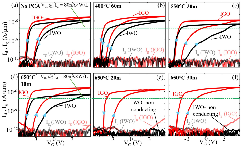
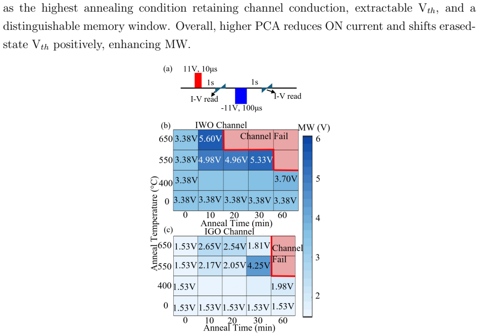
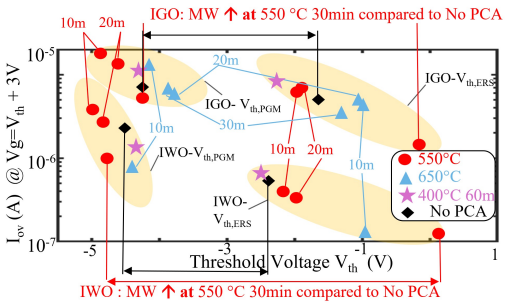
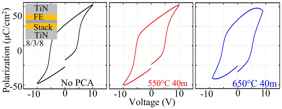
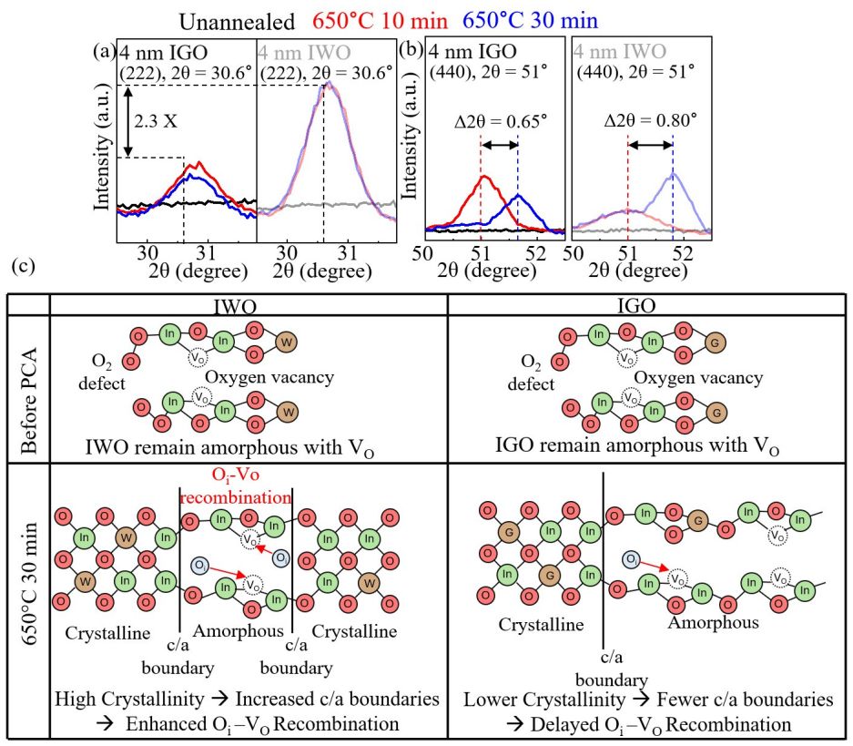
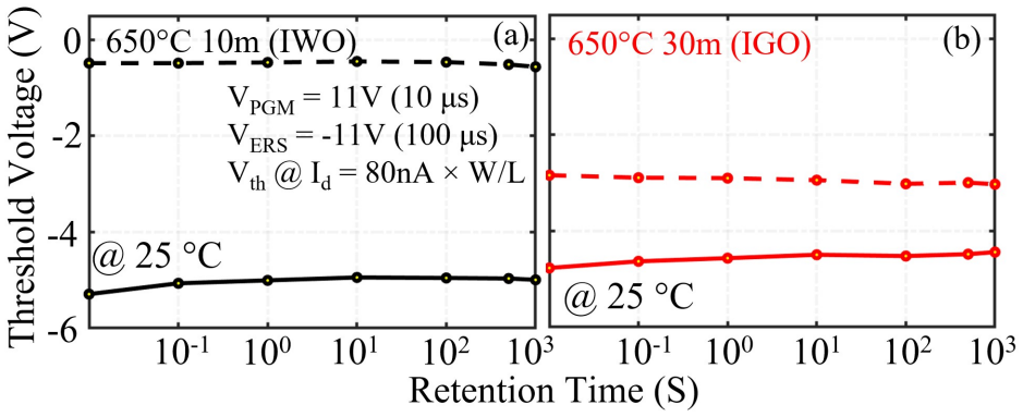
Using an identical ferroelectric gate stack of 8nm HZO / 3nm Al2O3 / 8nm HZO and a hybrid capping layer, the 10 percent Ga doped InO channel and 4 percent W doped InO channel FeFETs remain functional after annealing at temperatures up to 650 C for durations of up to 30 min and 10 min, respectively; further annealing results in irreversible loss of conduction and device failure. The MW enhancement originates from a preferential positive shift in the erased-state threshold voltage, while the programmed-state threshold voltage remains comparatively stable, with grazing-incidence X-ray diffraction measurements indicating structural evolution in the oxide channels.
What carries the argument
The doped indium oxide channels (10% Ga-doped InO and 4% W-doped InO) whose structural evolution under annealing sets the thermal processing limits, isolated by the hybrid capping layer and ferroelectric gate stack.
If this is right
- Memory window enhancement via erased-state threshold voltage shift remains achievable within the stated annealing budgets.
- The channels support post-capping thermal steps up to 650 C without immediate loss of conduction.
- Further temperature or time increases trigger irreversible channel degradation visible in both electrical and diffraction data.
- Structural changes in the oxide channels are the dominant factor setting the upper thermal bound for these FeFETs.
Where Pith is reading between the lines
- Different doping percentages in similar indium oxide channels could shift the observed temperature and time limits under the same stack conditions.
- The results point toward channel composition as a lever for matching FeFETs to fabrication flows with higher thermal budgets.
- Comparable capping strategies applied to other oxide channels would likely reveal material-specific thermal ceilings.
Load-bearing premise
The hybrid capping layer and identical ferroelectric gate stack isolate thermal effects to the oxide channels, such that observed threshold voltage shifts and device failure are attributable to channel structural evolution rather than capping or stack degradation.
What would settle it
Annealing devices that lack the hybrid capping layer or use a different gate stack and checking whether failure occurs at the same temperatures and times would test whether the channel alone drives the limits.
Figures
read the original abstract
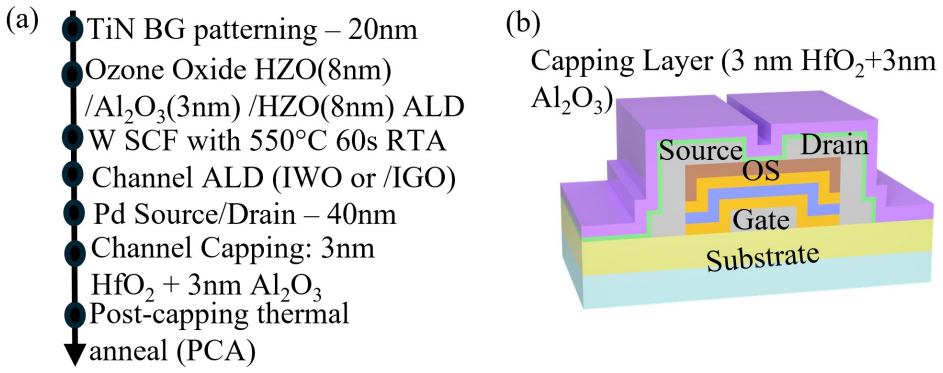
In this work, we report a systematic study of the impact of high-temperature post-capping thermal annealing on the memory characteristics of Oxide-semiconductor channel ferroelectric field-effect transistors (OS-FeFETs). Using an identical engineered ferroelectric gate stack 8nm Hf0.5Zr0.5O2 (HZO) / 3 nm Al2O3 / 8 nm HZO (8/3/8) and a hybrid capping layer (3 nm HfO2 + 3 nm Al2O3), 10 percent Ga doped InO (IGO) channel and 4 percent W doped InO (IWO) channel FeFETs remain functional after annealing at temperatures up to 650 C for durations of up to 30 min and 10 min, respectively; further annealing results in irreversible loss of conduction and device failure. Detailed electrical analysis reveals that the MW enhancement originates from a preferential positive shift in the erased-state threshold voltage, while the programmed-state threshold voltage remains comparatively stable. Grazing-incidence X-ray diffraction measurements further indicate structural evolution in the IWO and IGO oxide channels with increasing annealing temperature, supporting the observed electrical trends.
Editorial analysis
A structured set of objections, weighed in public.
Referee Report
Summary. The manuscript reports a study of post-capping thermal annealing effects on oxide-semiconductor channel FeFETs using an identical 8/3/8 HZO/Al2O3/HZO ferroelectric gate stack and hybrid HfO2/Al2O3 capping layer. It claims that 10% Ga-doped InO (IGO) and 4% W-doped InO (IWO) channel devices remain functional after annealing up to 650°C (30 min for IGO, 10 min for IWO), with memory window enhancement arising from preferential positive shifts in erased-state threshold voltage; further annealing causes irreversible loss of conduction attributed to channel structural evolution, supported by grazing-incidence XRD trends.
Significance. If the attribution of electrical degradation solely to channel evolution is confirmed, the work establishes practical thermal processing limits for OS-FeFET integration, which is relevant for back-end-of-line compatibility in ferroelectric memory. The correlation between GIXRD structural changes and VT/MW trends provides a useful experimental link, though the absence of full datasets limits the strength of the conclusions.
major comments (2)
- [Abstract] Abstract and electrical analysis sections: The central attribution of device failure after 650°C annealing to IGO/IWO channel structural evolution (supported by GIXRD) assumes the fixed 8/3/8 HZO/Al2O3/HZO ferroelectric stack and hybrid capping layer remain electrically intact. No post-anneal P-E hysteresis, C-V, or leakage data on the gate stack itself are described to isolate channel effects from possible stack degradation.
- [Abstract] Abstract: The reported electrical trends (MW enhancement from erased-state VT shift, irreversible conduction loss) are described as arising from detailed analysis, but the manuscript lacks full datasets, error bars, statistical details, or exclusion criteria, leaving the robustness of the cross-temperature claims moderately supported at best.
Simulated Author's Rebuttal
We thank the referee for the careful review and valuable comments on our manuscript. We address each major comment below.
read point-by-point responses
-
Referee: [Abstract] Abstract and electrical analysis sections: The central attribution of device failure after 650°C annealing to IGO/IWO channel structural evolution (supported by GIXRD) assumes the fixed 8/3/8 HZO/Al2O3/HZO ferroelectric stack and hybrid capping layer remain electrically intact. No post-anneal P-E hysteresis, C-V, or leakage data on the gate stack itself are described to isolate channel effects from possible stack degradation.
Authors: This is an important point. However, since the gate stack is identical for both IGO and IWO channel devices, and the maximum annealing temperature and time before failure differ between the two channel materials (650°C for 30 min in IGO vs. 10 min in IWO), the degradation cannot be attributed to the gate stack, which would affect both similarly. The correlation with channel-specific GIXRD changes further supports our interpretation. We will add this clarification to the revised manuscript to strengthen the argument. revision: partial
-
Referee: [Abstract] Abstract: The reported electrical trends (MW enhancement from erased-state VT shift, irreversible conduction loss) are described as arising from detailed analysis, but the manuscript lacks full datasets, error bars, statistical details, or exclusion criteria, leaving the robustness of the cross-temperature claims moderately supported at best.
Authors: We agree that including more comprehensive data presentation will improve the manuscript. In the revision, we will add error bars to the relevant plots, specify the number of devices measured at each temperature, and include details on the analysis methods and any data exclusion criteria used. revision: yes
Circularity Check
No circularity: purely experimental report with no derivations or models
full rationale
The manuscript is an experimental study reporting measured electrical characteristics (threshold voltage shifts, memory window) and GIXRD data on annealed OS-FeFET devices. No equations, fitted parameters, predictions, or theoretical derivations appear in the provided text or abstract. Claims rest on direct observation of device behavior before/after annealing and structural measurements; the attribution of trends to channel evolution is an interpretive conclusion from data, not a self-referential reduction. No self-citations, ansatzes, or uniqueness theorems are invoked in any load-bearing step. The derivation chain is empty by construction, satisfying the default expectation of no circularity for experimental reports.
Axiom & Free-Parameter Ledger
axioms (1)
- domain assumption Electrical characterization and grazing-incidence X-ray diffraction accurately capture threshold voltage shifts and structural evolution without significant artifacts.
Reference graph
Works this paper leans on
-
[1]
Advances in emerging memory technologies: From data storage to artificial intelligence,
G. Molas and E. Nowak, “Advances in emerging memory technologies: From data storage to artificial intelligence,”Applied Sciences, vol. 11, no. 23, p. 11254, 2021
2021
-
[2]
The fundamentals of nand flash memory: Technology for tomorrow’s fourth industrial revolution,
C.-W. Yoon, “The fundamentals of nand flash memory: Technology for tomorrow’s fourth industrial revolution,”IEEE Solid-State Circuits Magazine, vol. 14, no. 2, pp. 56–65, 2022
2022
-
[3]
Prospective innovation of dram, flash, and logic technologies for digital transformation (dx) era,
D. Ha and H.-S. Kim, “Prospective innovation of dram, flash, and logic technologies for digital transformation (dx) era,” in2022 IEEE Symposium on VLSI Technology and Circuits (VLSI Technology and Circuits), 2022, pp. 417–418
2022
-
[4]
Improve- ment of thermal stability in dual mechanism memory using hf x al 1-x o blocking layer for 3d v-nand flash application,
J. H. Chu, S. H. Kim, C. Kang, E. J. Shin, J. Jeong, Y. Park, and B. J. Cho, “Improve- ment of thermal stability in dual mechanism memory using hf x al 1-x o blocking layer for 3d v-nand flash application,”IEEE Electron Device Letters, 2024. 9
2024
-
[5]
Comprehensive design guidelines of gate stack for qlc and highly reliable ferroelectric vnand,
S. Lim, T. Kim, I. Myeong, S. Park, S. Noh, S. M. Lee, J. Woo, H. Ko, Y. Noh, M. Choiet al., “Comprehensive design guidelines of gate stack for qlc and highly reliable ferroelectric vnand,” in2023 International Electron Devices Meeting (IEDM). IEEE, 2023, pp. 1–4
2023
-
[6]
Vertical ferroelectric hfo 2 fet based on 3-d nand architecture: Towards dense low-power memory,
K. Florent, M. Pesic, A. Subirats, K. Banerjee, S. Lavizzari, A. Arreghini, L. Di Piazza, G. Potoms, F. Sebaai, S. McMitchellet al., “Vertical ferroelectric hfo 2 fet based on 3-d nand architecture: Towards dense low-power memory,” in2018 IEEE International Electron Devices Meeting (IEDM). IEEE, 2018, pp. 2–5
2018
-
[7]
Superior qlc retention (10 years, 85°c) and record memory window (12.2 v) by gate stack engineering in ferroelectric fet: from “mifis
S.-H. Kuk, B. H. Kim, Y. Park, K. Ko, H.-S. Hwang, D. Lee, B. J. Cho, J.-H. Han, and S.-H. Kim, “Superior qlc retention (10 years, 85°c) and record memory window (12.2 v) by gate stack engineering in ferroelectric fet: from “mifis” to” mikfis”,” in2024 IEEE International Electron Devices Meeting (IEDM). IEEE, 2024, pp. 1–4
2024
-
[8]
Material choices for tunnel dielectric layer and gate blocking layer for ferroelectric nand applications,
L. Fernandes, P. Venkatesan Ravindran, T. Song, D. Das, C. Park, N. Afroze, M. Tian, H. Chen, W. Chern, K. Kim, J. Woo, S. Lim, K. Kim, W. Kim, D. Ha, S. Yu, S. Datta, and A. Khan, “Material choices for tunnel dielectric layer and gate blocking layer for ferroelectric nand applications,”IEEE Electron Device Letters, vol. 45, no. 10, pp. 1776–1779, 2024
2024
-
[9]
Pushing the limits of nand technology scaling with ferro- electrics,
P. Venkatesan, L. Fernandes, S. Kang, P. Ravikumar, T. Song, C. Park, D. Das, K. H. Kim, K. Seo, K. Kimet al., “Pushing the limits of nand technology scaling with ferro- electrics,”MRS Bulletin, pp. 1–14, 2025
2025
-
[10]
Ferroelectric transistors for low-power nand flash memory,
S. Yoo, T. J. Kim, S.-G. Nam, D. Kim, K. Kim, Y. Lee, M. Jung, K.-H. Lee, S. Choi, S. D. Hyunet al., “Ferroelectric transistors for low-power nand flash memory,”Nature, vol. 648, no. 8093, pp. 320–326, 2025
2025
-
[11]
H. Joh, G. Kim, J. Ock, S. Kim, S. Lee, S. Lee, K. Kim, S. Lim, J. Woo, W. Kim et al., “Oxide channel ferroelectric nand device with source-tied covering metal struc- ture: Wide memory window (14.3 v), reliable retention (10 years) and disturbance immunity 0.1v for qlc operation,” in2024 IEEE International Electron Devices Meeting (IEDM). IEEE, 2024, pp. 1–4
2024
-
[12]
Comparative study of channel materials for ferroelectric nand applications,
L. Fernandes, P. Venkatesan, M. Tian, Y.-H. Kuo, N. Afroze, S. Soliman, S. Kang, D. Chakraborty, T. Song, C. Zhanget al., “Comparative study of channel materials for ferroelectric nand applications,” in2025 IEEE International Memory Workshop (IMW). IEEE, 2025, pp. 1–4. 10
2025
-
[13]
Experiments and modeling of defect dynamics and bti behavior in doped ino tfts during 400°c postprocessing forming gas annealing,
Y.-H. Kuo, C. Zhang, P. Ravikumar, S. Kang, T. Song, M. Villena, L. Larcher, H. Kim, M. Hong, P. Yun, G. Thareja, S. Yu, D. Ha, S. Datta, J. Medvedeva, and A. Khan, “Experiments and modeling of defect dynamics and bti behavior in doped ino tfts during 400°c postprocessing forming gas annealing,”IEEE Transactions on Electron Devices, pp. 1–9, 2026
2026
-
[14]
Analysis of the contact resistance in amorphous ingazno thin film transistors,
W. Wang, L. Li, C. Lu, Y. Liu, H. Lv, G. Xu, Z. Ji, and M. Liu, “Analysis of the contact resistance in amorphous ingazno thin film transistors,”Applied Physics Letters, vol. 107, no. 6, 2015
2015
-
[15]
Specific contact resistances between amorphous oxide semiconductor in–ga–zn–o and metallic electrodes,
Y. Shimura, K. Nomura, H. Yanagi, T. Kamiya, M. Hirano, and H. Hosono, “Specific contact resistances between amorphous oxide semiconductor in–ga–zn–o and metallic electrodes,”Thin Solid Films, vol. 516, no. 17, pp. 5899–5902, 2008
2008
-
[16]
First beol-compatible igzo ferroelectic-modulated diode with drastically enhanced memory window: Experiment, modeling, and deep understanding,
L. Jiao, Z. Zhou, Z. Zheng, K. Han, Q. Kong, X. Wang, H. Xu, J. Zhang, C. Sun, Y. Kang, G. Liang, and X. Gong, “First beol-compatible igzo ferroelectic-modulated diode with drastically enhanced memory window: Experiment, modeling, and deep understanding,” in2023 International Electron Devices Meeting (IEDM), 2023, pp. 1– 4
2023
-
[17]
Systematic investigation on the effect of contact resistance on the performance of a-igzo thin-film transistors with various geometries of electrodes,
J. S. Lee, S. Chang, H. Bouzid, S.-M. Koo, and S. Y. Lee, “Systematic investigation on the effect of contact resistance on the performance of a-igzo thin-film transistors with various geometries of electrodes,”physica status solidi (a), vol. 207, no. 7, pp. 1694–1697, 2010
2010
-
[18]
Elucidating the role of hydrogen at c-in2o3/a- in2o3- x interface,
J. E. Medvedeva and M. I. Bertoni, “Elucidating the role of hydrogen at c-in2o3/a- in2o3- x interface,”physica status solidi (RRL)–Rapid Research Letters, vol. 19, no. 11, p. 2500068, 2025
2025
-
[19]
Hydrogen behavior at crystalline/amorphous interface of transparent oxide semiconductor and its effects on carrier transport and crystallization,
J. E. Medvedeva, K. Sharma, B. Bhattarai, and M. I. Bertoni, “Hydrogen behavior at crystalline/amorphous interface of transparent oxide semiconductor and its effects on carrier transport and crystallization,”ACS applied materials & interfaces, vol. 14, no. 34, pp. 39 535–39 547, 2022. 11
2022
discussion (0)
Sign in with ORCID, Apple, or X to comment. Anyone can read and Pith papers without signing in.