Filamentary Transport and Thermoelectric Effects in Mushroom Phase Change Memory Cells
Pith reviewed 2026-06-27 11:16 UTC · model grok-4.3
The pith
Reset operations in mushroom phase change memory cells require three times less energy when current flows from top electrode to narrow bottom electrode due to thermoelectric effects.
A machine-rendered reading of the paper's core claim, the machinery that carries it, and where it could break.
Core claim
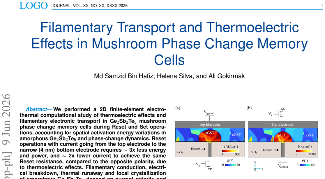
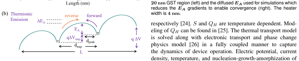
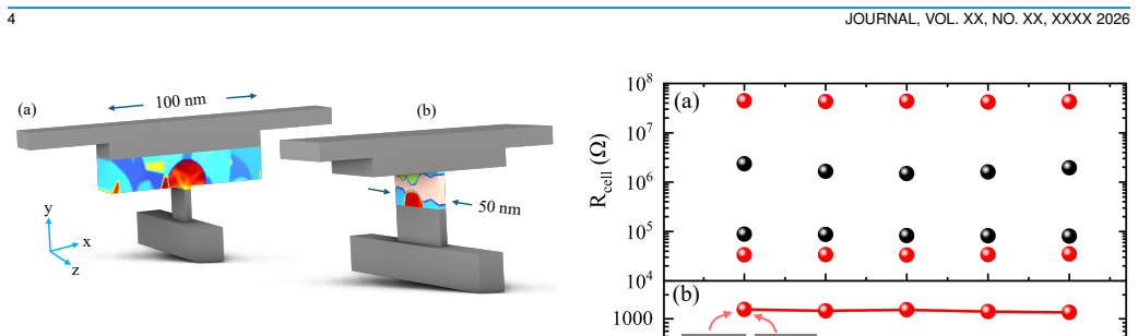
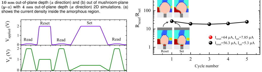
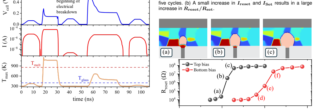
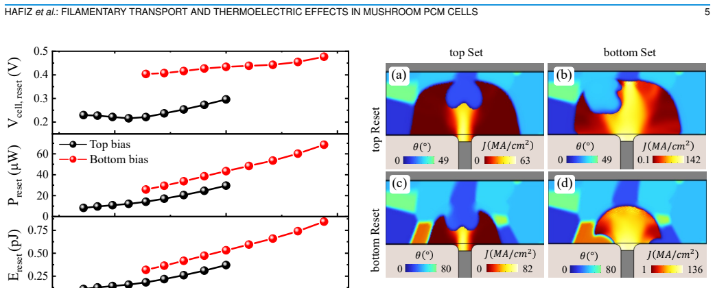
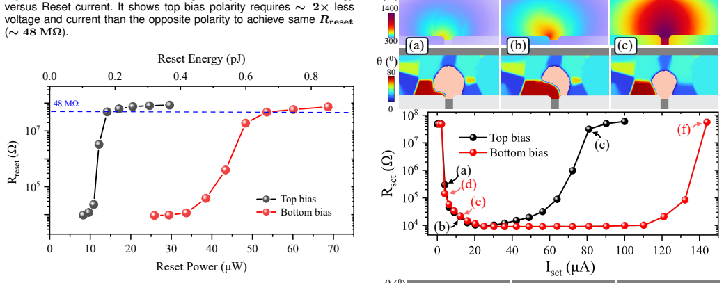
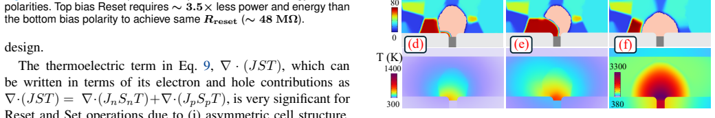
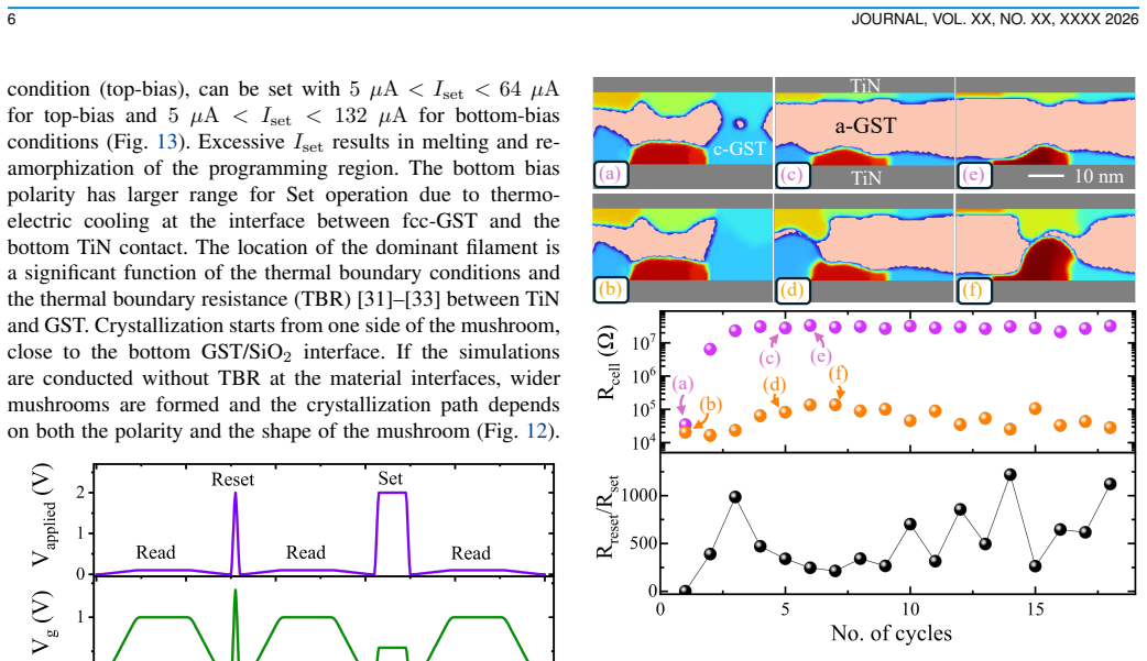
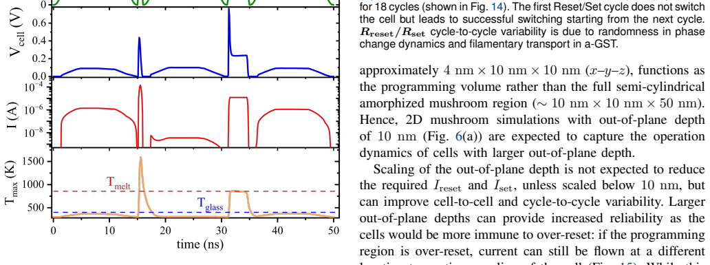
Reset operations with current going from the top electrode to the narrow 4 nm bottom electrode require ∼3x less energy and power, and ∼2x lower current to achieve the same Reset resistance, compared to the opposite polarity, due to thermoelectric effects. Filamentary conduction, electrical breakdown, thermal runaway, and local crystallization of amorphous Ge2Sb2Te5 depend on current polarity and thermal boundary conditions, and determine the location, shape, and volume of the programming region, which may be significantly smaller than the semi-cylindrical mushroom region. The programming volume does not scale with contact dimensions larger than 10 nm.
What carries the argument
2D finite-element electrothermal model incorporating spatial activation energy variations in amorphous Ge2Sb2Te5 together with phase-change dynamics.
Load-bearing premise
The 2D finite-element electrothermal model with spatial activation energy variations accurately captures filamentary conduction, thermal runaway, and phase-change dynamics in the amorphous material.
What would settle it
Fabricate mushroom cells with 4 nm bottom electrodes, measure reset energy and current for both polarities, and check whether one direction consistently requires roughly three times less energy to reach the target resistance.
Figures
read the original abstract
We performed a 2D finite-element electrothermal computational study of thermoelectric effects and filamentary electronic transport in Ge$_2$Sb$_2$Te$_5$ mushroom phase change memory cells during Reset and Set operations, accounting for spatial activation energy variations in amorphous Ge$_2$Sb$_2$Te$_5$ and phase-change dynamics. Reset operations with current going from the top electrode to the narrow 4 nm bottom electrode require $\sim$3x less energy and power, and $\sim$2x lower current to achieve the same Reset resistance, compared to the opposite polarity, due to thermoelectric effects. Filamentary conduction, electrical breakdown, thermal runaway, and local crystallization of amorphous Ge$_2$Sb$_2$Te$_5$ depend on current polarity and thermal boundary conditions, and determine the location, shape, and volume of the programming region, which may be significantly smaller than the semi-cylindrical mushroom region. The programming volume does not scale with contact dimensions larger than 10 nm. Larger contact areas introduce increased device-to-device and cycle-to-cycle variability due to filamentary conduction but are expected to lead to higher reliability and endurance.
Editorial analysis
A structured set of objections, weighed in public.
Referee Report
Summary. The manuscript reports a 2D finite-element electrothermal simulation of filamentary electronic transport and thermoelectric effects in Ge₂Sb₂Te₅ mushroom phase-change memory cells. It claims that reset operations with current flowing from the top electrode to the narrow 4 nm bottom electrode require ∼3× less energy and power and ∼2× lower current to reach the same reset resistance than the opposite polarity, due to thermoelectric effects. Additional findings address polarity-dependent filamentary conduction, thermal runaway, local crystallization, the resulting programming volume (which may be smaller than the mushroom region and does not scale for contacts >10 nm), and increased device-to-device variability for larger contacts.
Significance. If the model predictions are reliable, the work supplies concrete design guidance on polarity selection for reduced programming energy in PCM cells and clarifies how filamentary transport governs programming volume and variability, both of which are practically relevant for scaling and endurance of phase-change memory.
major comments (2)
- [Abstract] Abstract: the quantitative factors (∼3× energy/power, ∼2× current) are stated as direct outcomes of the simulation, yet the manuscript supplies no mesh-convergence data, parameter-sensitivity study on the spatial activation-energy variations, or uncertainty quantification; these omissions are load-bearing for the central numerical claims.
- [Model description (implied by abstract)] The 2D finite-element model is used to predict 3D filamentary behavior and thermal-runaway dynamics without reported validation against experimental reset/set characteristics or against a 3D reference simulation; this directly affects in the predicted polarity asymmetry and programming-volume conclusions.
minor comments (2)
- Notation for the bottom-electrode diameter (stated as 4 nm) and contact-area scaling (>10 nm) should be cross-checked for consistency with the figures that illustrate the mushroom geometry.
- The abstract states that the programming volume 'may be significantly smaller than the semi-cylindrical mushroom region'; a quantitative comparison (e.g., volume ratio) in the results section would strengthen this statement.
Simulated Author's Rebuttal
We thank the referee for the constructive comments on our manuscript. We address each major comment below and indicate the revisions we will make to strengthen the work.
read point-by-point responses
-
Referee: [Abstract] Abstract: the quantitative factors (∼3× energy/power, ∼2× current) are stated as direct outcomes of the simulation, yet the manuscript supplies no mesh-convergence data, parameter-sensitivity study on the spatial activation-energy variations, or uncertainty quantification; these omissions are load-bearing for the central numerical claims.
Authors: We agree that explicit mesh-convergence data, sensitivity analysis on activation-energy spatial variations, and uncertainty quantification would strengthen the quantitative claims. In the revised manuscript we will add a mesh-convergence study in the Methods section demonstrating that the reported factors remain stable under successive refinement. We will also include a parameter-sensitivity analysis varying the activation-energy profile within literature-reported bounds and report the resulting variation in the polarity asymmetry factors. Basic uncertainty estimates derived from these variations will be provided alongside the central claims. revision: yes
-
Referee: [Model description (implied by abstract)] The 2D finite-element model is used to predict 3D filamentary behavior and thermal-runaway dynamics without reported validation against experimental reset/set characteristics or against a 3D reference simulation; this directly affects in the predicted polarity asymmetry and programming-volume conclusions.
Authors: The 2D axisymmetric model is selected to resolve the essential radial and axial transport governing filament formation and thermoelectric asymmetry while remaining computationally tractable. Model parameters are taken from established GST literature. We acknowledge that direct experimental validation and a full 3D reference simulation are absent. In revision we will add an explicit Limitations subsection discussing the 2D approximation, its expected impact on filamentary volume and thermal-runaway thresholds, and comparisons to any available 3D literature results. We will also clarify that the polarity asymmetry originates from the Seebeck/Peltier terms, which are dimension-independent in the governing equations. revision: partial
Circularity Check
No significant circularity
full rationale
The paper reports quantitative outcomes (~3x energy reduction, ~2x current reduction) as direct numerical results from a 2D finite-element electrothermal simulation that incorporates thermoelectric effects, spatial activation-energy variations, and phase-change dynamics as inputs. No step in the described chain reduces a claimed prediction to a fitted parameter or self-citation by construction; the model is physics-based and the polarity asymmetry is an emergent output rather than an input. The derivation is therefore self-contained against external benchmarks.
Axiom & Free-Parameter Ledger
Reference graph
Works this paper leans on
-
[1]
Designing crystalliza- tion in phase-change materials for universal memory and neuro-inspired computing,
W. Zhang, R. Mazzarello, M. Wuttig, and E. Ma, “Designing crystalliza- tion in phase-change materials for universal memory and neuro-inspired computing,”Nature Reviews Materials, vol. 4, pp. 150–168, 2019
2019
-
[2]
Recent progress in phase-change memory technology,
G. W. Burr, M. J. BrightSky, A. Sebastian, H.-Y . Cheng, J.-Y . Wu, S. Kim, N. E. Sosa, N. Papandreou, H.-L. Lung, H. Pozidiset al., “Recent progress in phase-change memory technology,”IEEE Journal on Emerging and Selected Topics in Circuits and Systems, vol. 6, no. 2, pp. 146–162, 2016
2016
-
[3]
Material and process engineering challenges in ge-rich gst for embedded pcm,
A. Redaelli, E. Petroni, and R. Annunziata, “Material and process engineering challenges in ge-rich gst for embedded pcm,”Materials Science in Semiconductor Processing, vol. 137, p. 106184, 2022
2022
-
[4]
Phase change memory for automotive grade embedded NVM applications,
P. Cappelletti, R. Annunziata, F. Arnaud, F. Disegni, A. Maurelli, and P. Zuliani, “Phase change memory for automotive grade embedded NVM applications,”Journal of Physics D: Applied Physics, vol. 53, no. 19, p. 193002, 2020
2020
-
[5]
Modeling of SET and reset operations of phase-change memory cells,
A. Faraclas, N. Williams, A. Gokirmak, and H. Silva, “Modeling of SET and reset operations of phase-change memory cells,”IEEE Electron Device Letters, vol. 32, no. 12, pp. 1737–1739, 2011
2011
-
[6]
Modeling filamentary conduction in reset phase change memory devices,
M. S. B. Hafiz, H. Silva, and A. Gokirmak, “Modeling filamentary conduction in reset phase change memory devices,”physica status solidi (RRL) – Rapid Research Letters, p. 2400416, 2025
2025
-
[7]
Phase change materials and phase change memory,
S. Raoux, F. Xiong, M. Wuttig, and E. Pop, “Phase change materials and phase change memory,”MRS Bulletin, vol. 39, no. 8, pp. 703–710, 2014
2014
-
[8]
Phase-change random access memory: A scalable technology,
S. Raoux, G. W. Burr, M. J. Breitwisch, C. T. Rettner, Y .-C. Chen, R. M. Shelby, M. Salinga, D. Krebs, S.-H. Chen, H.-L. Lung, and C. H. Lam, “Phase-change random access memory: A scalable technology,”IBM Journal of Research and Development, vol. 52, no. 4.5, pp. 465–479, 2008
2008
-
[9]
Observation and modelling of homogeneous nucleation in ge 2sb2te5 mushroom cells during set operation,
Y . Yu and M. Skowronski, “Observation and modelling of homogeneous nucleation in ge 2sb2te5 mushroom cells during set operation,”Journal of Materials Chemistry C, vol. 11, no. 11, pp. 3848–3854, 2023
2023
-
[10]
3d cross-point phase-change memory for storage-class memory,
H.-Y . Cheng, F. Carta, W.-C. Chien, H.-L. Lung, and M. J. BrightSky, “3d cross-point phase-change memory for storage-class memory,”Jour- nal of Physics D: Applied Physics, vol. 52, no. 47, p. 473002, 2019
2019
-
[11]
Ielmini,Phase Change Memory: Device Physics, Reliability and Applications
D. Ielmini,Phase Change Memory: Device Physics, Reliability and Applications. Cham: Springer, 2018
2018
-
[12]
Threshold switching mechanism by high-field energy gain in the hopping transport of chalcogenide glasses,
D. Ielmini, “Threshold switching mechanism by high-field energy gain in the hopping transport of chalcogenide glasses,”Physical Review B, vol. 78, no. 3, p. 035308, 2008
2008
-
[13]
Recent progress in resistive random access memories: Materials, switching mechanisms, and performance,
F. Pan, S. Gao, C. Chen, C. Song, and F. Zeng, “Recent progress in resistive random access memories: Materials, switching mechanisms, and performance,”Materials Science and Engineering: R: Reports, vol. 83, pp. 1–59, 2014
2014
-
[14]
Electrical conduction in chalcogenide glasses of phase change memory,
M. Nardone, M. Simon, I. V . Karpov, and V . G. Karpov, “Electrical conduction in chalcogenide glasses of phase change memory,”Journal of Applied Physics, vol. 112, no. 7, p. 071101, 2012
2012
-
[15]
High speed, high temperature electrical characterization of phase change materi- als: metastable phases, crystallization dynamics, and resistance drift,
F. Dirisaglik, G. Bakan, Z. Jurado, S. Muneer, M. Akbulut, J. Rarey, L. Sullivan, M. Wennberg, A. King, L. Zhanget al., “High speed, high temperature electrical characterization of phase change materi- als: metastable phases, crystallization dynamics, and resistance drift,” Nanoscale, vol. 7, no. 40, pp. 16 625–16 630, 2015
2015
-
[16]
Electrical resistivity of liquid Ge2Sb2Te5 based on thin-film and nanoscale device measurements,
K. Cilet al., “Electrical resistivity of liquid Ge2Sb2Te5 based on thin-film and nanoscale device measurements,”IEEE Transactions on Electron Devices, vol. 60, no. 1, pp. 433–437, 2013
2013
-
[17]
Activation energy of metastable amorphous Ge2Sb2Te5 from room temperature to melt,
S. Muneer, J. Scoggin, F. Dirisaglik, L. Adnane, A. Cywar, G. Bakan, K. Cil, C. Lam, H. Silva, and A. Gokirmak, “Activation energy of metastable amorphous Ge2Sb2Te5 from room temperature to melt,”AIP Advances, vol. 8, no. 6, p. 065314, 2018
2018
-
[18]
R. S. Khan, A. H. Talukder, F. Dirisaglik, H. Silva, and A. Gokirmak, “Accelerating and stopping resistance drift in phase change memory cells via high electric field stress,”arXiv preprint arXiv:2002.12487, 2020
arXiv 2002
-
[19]
M. Tashfiq, B. Kashem, R. S. Khan, A. H. Talukder, F. Dirisaglik, and A. Gokirmak, “Stopping resistance drift in phase change memory cells and analysis of charge transport in stable amorphous Ge2Sb2Te5,”arXiv preprint arXiv:2210.14035, 2022
arXiv 2022
-
[20]
Amorphous silicon thin film transistors,
J. L. Lin and S. C. Lee, “Amorphous silicon thin film transistors,” Journal of the Chinese Institute of Engineers, vol. 18, no. 4, pp. 451– 460, 1995
1995
-
[21]
Measurements of charge carrier mobilities and drift velocity saturation in bulk silicon of <111> and <100> crystal orientation at high electric fields,
J. Becker, E. Fretwurst, and R. Klanner, “Measurements of charge carrier mobilities and drift velocity saturation in bulk silicon of <111> and <100> crystal orientation at high electric fields,”Solid-State Electronics, vol. 56, no. 1, pp. 104–110, 2010
2010
-
[22]
Electrical measurement setup for phase-change materials,
L. Adnane, A. Gokirmak, and H. Silva, “Electrical measurement setup for phase-change materials,”Review of Scientific Instruments, vol. 87, p. 075117, 2016
2016
-
[23]
Modeling of phase-change memory: Nucleation, growth, and amorphization dynamics during SET and reset,
Z. Woods and A. Gokirmak, “Modeling of phase-change memory: Nucleation, growth, and amorphization dynamics during SET and reset,” IEEE Transactions on Electron Devices, vol. 64, no. 11, pp. 4466–4471, 2017
2017
-
[24]
Phonon and electron transport through Ge2Sb2Te5 films and interfaces bounded by metals,
J. Lee, E. Bozorg-Grayeli, S. Kim, M. Asheghi, H.-S. P. Wong, and K. E. Goodson, “Phonon and electron transport through Ge2Sb2Te5 films and interfaces bounded by metals,”Applied Physics Letters, vol. 102, no. 19, p. 191911, 2013
2013
-
[25]
Modeling and impacts of the latent heat of phase change and specific heat for phase change materials,
J. Scoggin, R. S. Khan, H. Silva, and A. Gokirmak, “Modeling and impacts of the latent heat of phase change and specific heat for phase change materials,”Applied Physics Letters, vol. 112, no. 19, p. 193502, 2018
2018
-
[26]
Modeling hetero- geneous melting in phase change memory devices,
J. Scoggin, Z. Woods, H. Silva, and A. Gokirmak, “Modeling hetero- geneous melting in phase change memory devices,”Applied Physics Letters, vol. 114, no. 4, p. 043502, 2019
2019
-
[27]
Impact of thermoelectric effects on phase change memory characteristics,
N. Ciocchini, M. Laudato, A. Leone, P. Fantini, A. L. Lacaita, and D. Ielmini, “Impact of thermoelectric effects on phase change memory characteristics,”IEEE Transactions on Electron Devices, vol. 62, no. 10, pp. 3264–3271, 2015
2015
-
[28]
Modeling of thermoelectric effects in phase change memory cells,
A. Faraclas, G. Bakan, L. Adnane, F. Dirisaglik, N. E. Williams, A. Gokirmak, and H. Silva, “Modeling of thermoelectric effects in phase change memory cells,”IEEE Transactions on Electron Devices, vol. 61, no. 2, pp. 372–378, 2014
2014
-
[29]
(digital presentation) finite element modeling of thermoelectric effects in phase change memory cells,
M. T. B. Kashem, J. Scoggin, H. Silva, and A. Gokirmak, “(digital presentation) finite element modeling of thermoelectric effects in phase change memory cells,”ECS Transactions, vol. 108, no. 1, pp. 3–15, 2022
2022
-
[30]
High-temperature thermoelectric transport at small scales: Thermal generation, transport and recombination of minority carriers,
G. Bakan, N. Khan, H. Silva, and A. Gokirmak, “High-temperature thermoelectric transport at small scales: Thermal generation, transport and recombination of minority carriers,”Scientific Reports, vol. 3, no. 1, p. 2724, 2013
2013
-
[31]
Phonon and electron transport through Ge2Sb2Te5 films and interfaces bounded by metals,
J. Lee, E. Bozorg-Grayeli, S. Kim, M. Asheghi, H.-S. P. Wong, and K. E. Goodson, “Phonon and electron transport through Ge2Sb2Te5 films and interfaces bounded by metals,”Applied Physics Letters, vol. 102, p. 191911, 2013
2013
-
[32]
Thermal conductivity of phase-change memory materials from cryogenic temperatures to 400 k,
J. Lee, J. P. Reifenberg, E. Bozorg-Grayeli, L. Hom, Z. Li, S. B. Kim, M. Asheghi, H.-S. P. Wong, and K. E. Goodson, “Thermal conductivity of phase-change memory materials from cryogenic temperatures to 400 k,” in12th IEEE Intersociety Conference on Thermal and Thermome- chanical Phenomena in Electronic Systems, 2010, pp. 1–8
2010
-
[33]
Thermal boundary resistance measurements for phase-change memory devices,
J. P. Reifenberg, K.-W. Chang, M. A. Panzer, S. Kim, J. A. Rowlette, M. Asheghi, H.-S. P. Wong, and K. E. Goodson, “Thermal boundary resistance measurements for phase-change memory devices,”IEEE Electron Device Letters, vol. 31, no. 1, pp. 56–58, 2010
2010
discussion (0)
Sign in with ORCID, Apple, or X to comment. Anyone can read and Pith papers without signing in.