Hexagonal Boron Nitride Spin Defects for Quantum Photonics: Annealing-Free Generation by Krypton Ion Implantation
Pith reviewed 2026-06-26 07:07 UTC · model grok-4.3
The pith
Krypton ion implantation generates stable room-temperature near-IR spin defects in hBN without annealing.
A machine-rendered reading of the paper's core claim, the machinery that carries it, and where it could break.
Core claim
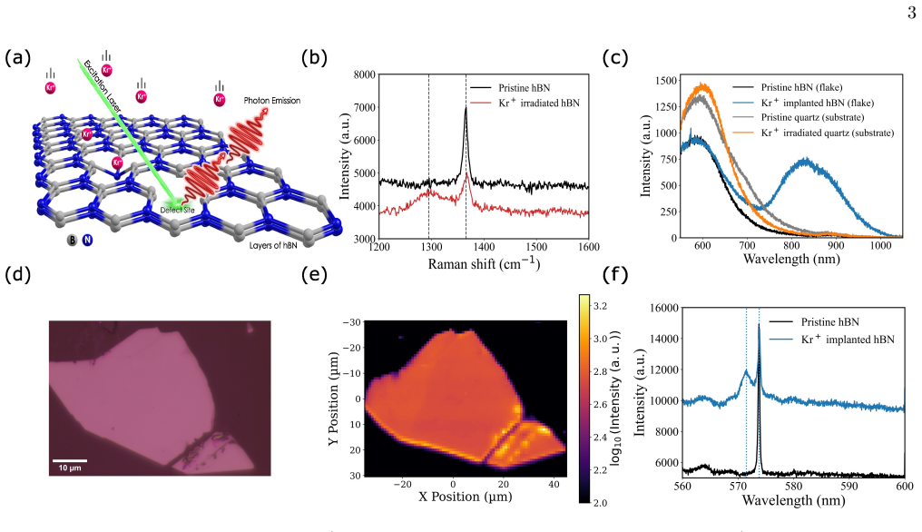
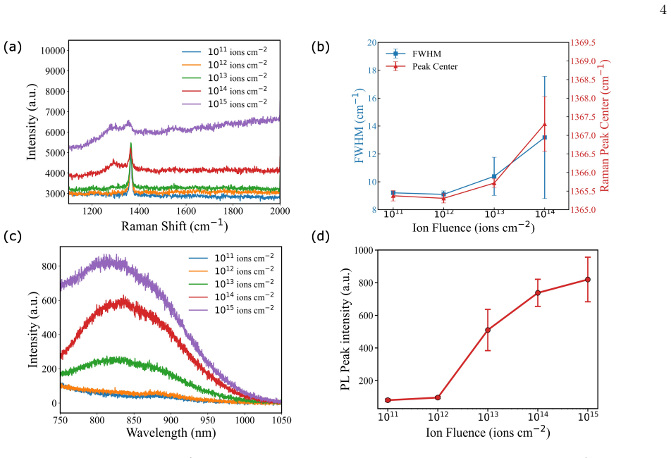
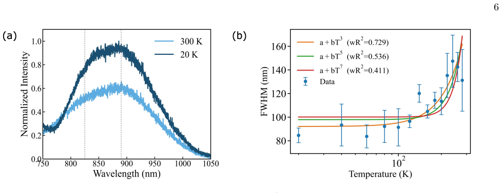
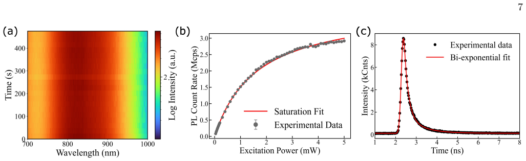
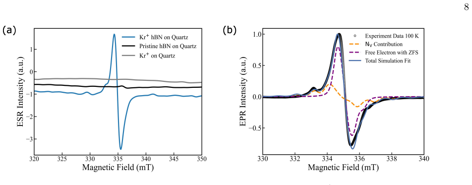
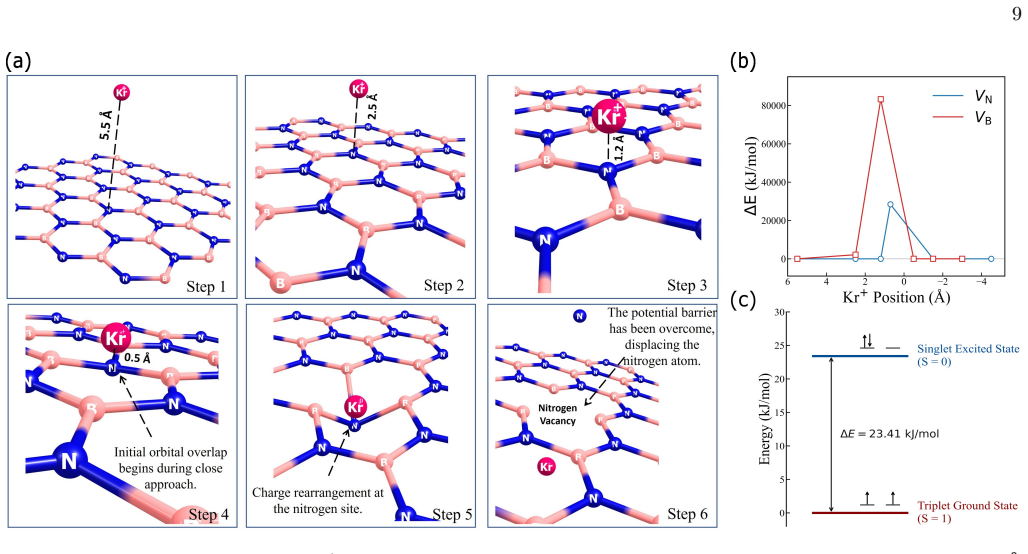
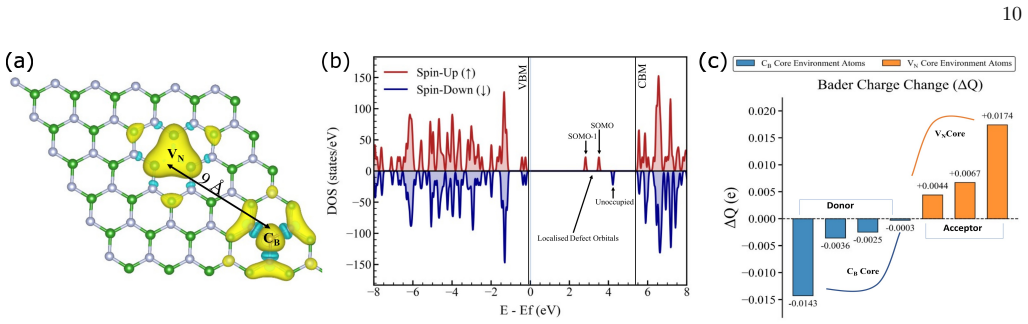
Kr+ ion implantation at 40 keV into hBN, performed without any pre- or post-implantation annealing, produces a stable near-infrared photoluminescence band centered at ~830 nm whose intensity increases with fluence over 10^11 to 10^15 ions/cm². The implanted material also shows an EPR signal with g-factor 2.003, and DFT calculations identify a spatially separated V_N-C_B donor-acceptor pair as a viable common origin for the observed optical and magnetic signatures. The PL linewidth broadens with temperature following a T^3 dependence, consistent with acoustic-phonon dephasing, while Raman spectra confirm irradiation-induced lattice disorder.
What carries the argument
Kr+ ion implantation into hBN flakes, with parameters chosen via SRIM Monte Carlo simulations, that directly introduces the lattice defects responsible for the near-IR luminescence and the g=2.003 paramagnetic center.
Load-bearing premise
The near-IR photoluminescence band and the EPR signal both originate from the same V_N-C_B donor-acceptor pair defect identified by the calculations.
What would settle it
Measuring whether the spatial map of 830 nm PL intensity across a single implanted flake matches the spatial distribution of the g=2.003 EPR signal strength would test whether the two signatures arise from the identical defect.
Figures
read the original abstract
Controlled, reproducible generation of luminescent defect centres in hBN remains a key challenge for scalable quantum-photonic technologies. Here, we report Kr$^{+}$ ion implantation as a tunable, annealing-free, and chemically inert route to room-temperature near-infrared luminescent spin defects in hBN, requiring no pre- or post-implantation annealing. SRIM Monte Carlo simulations were used to optimise the parameters for 40 keV Kr$^{+}$ irradiation of hBN flakes. The implanted samples exhibit a stable near-infrared photoluminescence (PL) band centred at $\sim$830 nm whose intensity increases with implantation fluence over $10^{11}$-$10^{15}$ions/cm$^{2}$. Temperature-dependent PL measurements (20-300 K) reveal a linewidth broadening well described by a $T^{3}$ dependence, consistent with acoustic-phonon-mediated dephasing. Raman spectra show the characteristic $E_{2g}$ mode of pristine hBN at $\sim$1366 cm$^{-1}$ alongside an implantation-induced defect feature at $\sim$1295 cm$^{-1}$, confirming irradiation-induced lattice disorder. Electron paramagnetic resonance (EPR) measurements reveal a paramagnetic centre with a $g$-factor of 2.003, and density functional theory (DFT) calculations indicate that a spatially separated $V_{\mathrm{N}}$-$C_{\mathrm{B}}$ donor-acceptor pair complex is a viable origin of the observed optical and magnetic signatures. Overall, Kr$^{+}$ implantation offers an effective, annealing-free, and scalable platform for generating stable room-temperature luminescent defects, providing a promising route toward quantum photonics.
Editorial analysis
A structured set of objections, weighed in public.
Referee Report
Summary. The manuscript claims that 40 keV Kr+ ion implantation into hBN, without pre- or post-annealing, generates stable room-temperature near-IR luminescent spin defects. PL intensity at ~830 nm scales with fluence (10^11–10^15 ions/cm²), linewidth follows T^3, Raman shows a ~1295 cm^{-1} defect mode, EPR yields g=2.003, and DFT identifies a spatially separated V_N-C_B donor-acceptor pair as the common origin, offering a scalable quantum-photonics platform.
Significance. If the optical, magnetic, and structural signatures are shown to arise from one defect, the annealing-free, chemically inert implantation route would be a practical advance for hBN-based quantum photonics. The work combines SRIM optimization, fluence-dependent PL, temperature-dependent linewidth, Raman, EPR, and DFT, providing a multi-technique experimental base.
major comments (2)
- [Abstract and PL/EPR results] The central assignment that the ~830 nm PL band and g=2.003 EPR signal originate from the same V_N-C_B defect is not supported by direct linkage. No fluence-dependent EPR spin-density data are shown to correlate with PL intensity, and no ODMR is reported to establish that the paramagnetic center is optically active at 830 nm (see Abstract and the PL/EPR results sections).
- [DFT calculations] The DFT claim that the spatially separated V_N-C_B pair accounts for both the observed optical transition (~1.5 eV) and the EPR g-factor requires quantitative comparison: calculated zero-phonon line or emission energy and g-tensor components should be shown to match experiment within stated uncertainties (DFT section).
minor comments (2)
- All PL, Raman, and EPR spectra and fluence plots should include error bars and explicit statements on baseline subtraction and background correction procedures.
- The manuscript should state the precise implantation energy, fluence values used for EPR, and any sample preparation details (e.g., flake thickness distribution) that affect SRIM predictions.
Simulated Author's Rebuttal
We thank the referee for the careful and constructive review of our manuscript. We address each major comment below with honest responses based on the data presented.
read point-by-point responses
-
Referee: [Abstract and PL/EPR results] The central assignment that the ~830 nm PL band and g=2.003 EPR signal originate from the same V_N-C_B defect is not supported by direct linkage. No fluence-dependent EPR spin-density data are shown to correlate with PL intensity, and no ODMR is reported to establish that the paramagnetic center is optically active at 830 nm (see Abstract and the PL/EPR results sections).
Authors: We agree that direct linkage via ODMR or fluence-dependent EPR spin density would provide stronger evidence. The manuscript presents the V_N-C_B pair as a viable origin based on the observed g=2.003 matching literature values for similar defects, the fluence-dependent PL scaling, and supporting Raman/DFT results. We will revise the abstract and discussion sections to clarify that this is a candidate assignment supported by multi-technique consistency rather than a definitive identification from direct correlation. No new EPR or ODMR data can be added without additional experiments. revision: partial
-
Referee: [DFT calculations] The DFT claim that the spatially separated V_N-C_B pair accounts for both the observed optical transition (~1.5 eV) and the EPR g-factor requires quantitative comparison: calculated zero-phonon line or emission energy and g-tensor components should be shown to match experiment within stated uncertainties (DFT section).
Authors: We accept this point. The current DFT discussion describes the pair as viable without quantitative matching. In the revision we will add the calculated emission energy (including ZPL) and g-tensor values from our simulations, directly compared to the experimental 1.5 eV and g=2.003, with explicit discussion of DFT uncertainties for defect levels in hBN. revision: yes
- Direct experimental linkage (fluence-dependent EPR or ODMR) between the PL band and EPR signal cannot be provided without new measurements outside the scope of this work.
Circularity Check
No circularity; experimental observations and DFT are independent
full rationale
The paper reports direct experimental results from Kr+ implantation (fluence-dependent PL at ~830 nm, Raman defect mode at ~1295 cm^{-1}, EPR at g=2.003) plus separate SRIM simulations for parameter choice and DFT modeling to suggest a V_N-C_B pair as a possible origin. None of these steps reduce a claimed prediction or first-principles result to the inputs by construction, nor rely on self-citation chains or fitted parameters renamed as outputs. The derivation chain is self-contained against external benchmarks with no load-bearing loops.
Axiom & Free-Parameter Ledger
free parameters (2)
- Implantation energy =
40 keV
- Fluence values =
10^11 to 10^15 ions/cm^2
axioms (1)
- domain assumption SRIM Monte Carlo code accurately models Kr+ stopping and vacancy production in hBN
invented entities (1)
-
Spatially separated V_N-C_B donor-acceptor pair
no independent evidence
Reference graph
Works this paper leans on
-
[1]
In compari- son, the T 5 and T 7 models yielded lower wR2 values of 0.536 and 0.411, respectively, together with higher AIC values of 23.96 and 29.30
The T 3 model provided the best description of the experimental data, yielding a = 92.11±3.15 nm and b = (3.18±0.57)×10−6nm K−3, with a weighted coef- ficient of determination of wR2 = 0.729 and an Akaike Information Criterion (AIC) value of 15.66. In compari- son, the T 5 and T 7 models yielded lower wR2 values of 0.536 and 0.411, respectively, together ...
2008
-
[2]
Quantum defects in two-dimensional van der waals materials.Fundamental Research, 2024
Yang Guo, Jianmei Li, Ruifen Dou, Haitao Ye, and Changzhi Gu. Quantum defects in two-dimensional van der waals materials.Fundamental Research, 2024
2024
-
[3]
Solid- state single-photon emitters.Nature photonics, 10(10):631– 641, 2016
Igor Aharonovich, Dirk Englund, and Milos Toth. Solid- state single-photon emitters.Nature photonics, 10(10):631– 641, 2016
2016
-
[4]
A perspective on solid-state quantum light sources: Materials and atomic defects.Nano Futures, May 2026
Anuj Kumar KUMAR Singh, Parul Sharma, Kishor Ku- mar Mandal, Lekshmi Eswaramoorthy, and Anshuman Kumar. A perspective on solid-state quantum light sources: Materials and atomic defects.Nano Futures, May 2026
2026
-
[5]
Atomically-thin single-photon sources for quantum communication.npj 2D Materials and Applications, 7(1):4, 2023
Timm Gao, Martin von Helversen, Carlos Ant´ on-Solanas, Christian Schneider, and Tobias Heindel. Atomically-thin single-photon sources for quantum communication.npj 2D Materials and Applications, 7(1):4, 2023
2023
-
[6]
Defects in hexagonal boron nitride for quantum technologies.arXiv preprint arXiv:2510.04344, 2025
Tobias Vogl, Viktor Iv´ ady, Isaac J Luxmoore, and Han- nah L Stern. Defects in hexagonal boron nitride for quantum technologies.arXiv preprint arXiv:2510.04344, 2025
arXiv 2025
-
[7]
Single photon sources in atomically thin materials.Annual review of physical chemistry, 70(1):123–142, 2019
Milos Toth and Igor Aharonovich. Single photon sources in atomically thin materials.Annual review of physical chemistry, 70(1):123–142, 2019
2019
-
[8]
Optical quantum technologies with hexagonal boron nitride single photon sources.Scientific reports, 11(1):12285, 2021
Akbar Basha Dhu-al-jalali-wal-ikram Shaik and Penchala- iah Palla. Optical quantum technologies with hexagonal boron nitride single photon sources.Scientific reports, 11(1):12285, 2021
2021
-
[9]
Defect and strain engineering of monolayer wse2 enables site-controlled single-photon emission up to 150 k.Nature communications, 12(1):3585, 2021
Kamyar Parto, Shaimaa I Azzam, Kaustav Banerjee, and Galan Moody. Defect and strain engineering of monolayer wse2 enables site-controlled single-photon emission up to 150 k.Nature communications, 12(1):3585, 2021
2021
-
[10]
H Kamada and T Kutsuwa. Broadening of single quan- tum dot exciton luminescence spectra due to interaction with randomly fluctuating environmental charges.Physi- cal Review B—Condensed Matter and Materials Physics, 78(15):155324, 2008
2008
-
[11]
Electron-phonon processes of the nitrogen-vacancy center in diamond.Physical Review B, 92(8):081203, 2015
Taras Plakhotnik, Marcus W Doherty, and Neil B Manson. Electron-phonon processes of the nitrogen-vacancy center in diamond.Physical Review B, 92(8):081203, 2015
2015
-
[12]
Plasmonic-strain engineering of quantum emit- ters in hexagonal boron nitride.Advanced Materials In- terfaces, 12(13):2500071, 2025
Anuj Kumar Singh, Utkarsh, Pablo Tieben, Kishor Ku- mar Mandal, Brijesh Kumar, Rishabh Vij, Amrita Ma- jumder, Ikshvaku Shyam, Shagun Kumar, Kenji Watan- abe, et al. Plasmonic-strain engineering of quantum emit- ters in hexagonal boron nitride.Advanced Materials In- terfaces, 12(13):2500071, 2025
2025
-
[13]
Single defect centres in diamond: A review.physica status solidi (a), 203(13):3207– 3225, 2006
Fedor Jelezko and J¨ org Wrachtrup. Single defect centres in diamond: A review.physica status solidi (a), 203(13):3207– 3225, 2006
2006
-
[14]
Creation and nature of optical centres in diamond for single-photon emission—overview and critical remarks.New Journal of Physics, 13(3):035024, 2011
S´ ebastien Pezzagna, Detlef Rogalla, Dominik Wildan- ger, Jan Meijer, and Alexander Zaitsev. Creation and nature of optical centres in diamond for single-photon emission—overview and critical remarks.New Journal of Physics, 13(3):035024, 2011
2011
-
[15]
Defect inspection techniques in sic.Nanoscale Research Letters, 17(1):30, 2022
Po-Chih Chen, Wen-Chien Miao, Tanveer Ahmed, Yi-Yu Pan, Chun-Liang Lin, Shih-Chen Chen, Hao-Chung Kuo, Bing-Yue Tsui, and Der-Hsien Lien. Defect inspection techniques in sic.Nanoscale Research Letters, 17(1):30, 2022
2022
-
[16]
Hexagonal boron nitride is an indirect bandgap semicon- ductor.Nature photonics, 10(4):262–266, 2016
Guillaume Cassabois, Pierre Valvin, and Bernard Gil. Hexagonal boron nitride is an indirect bandgap semicon- ductor.Nature photonics, 10(4):262–266, 2016
2016
-
[17]
Quantum optics applications of hexagonal boron nitride defects.Advanced Optical Materials, 13(7):2402508, 2025
AslıC ¸akan, Chanaprom Cholsuk, Angus Gale, Mehran Kianinia, Serkan Pa¸ cal, Serkan Ate¸ s, Igor Aharonovich, Milos Toth, and Tobias Vogl. Quantum optics applications of hexagonal boron nitride defects.Advanced Optical Materials, 13(7):2402508, 2025
2025
-
[18]
Quantum emission from hexagonal boron nitride monolayers.Nature nanotechnol- ogy, 11(1):37–41, 2016
Toan Trong Tran, Kerem Bray, Michael J Ford, Milos Toth, and Igor Aharonovich. Quantum emission from hexagonal boron nitride monolayers.Nature nanotechnol- ogy, 11(1):37–41, 2016
2016
-
[19]
Near-deterministic activation of room-temperature quan- tum emitters in hexagonal boron nitride.Nature Com- munications, 9:165, 2018
Nicholas Proscia, Geun Ho Ahn, Andreas W Schell, et al. Near-deterministic activation of room-temperature quan- tum emitters in hexagonal boron nitride.Nature Com- munications, 9:165, 2018
2018
-
[20]
Defect formation in hbn by plasma and chemical treatment: mechanisms and photophysical properties.Applied Physics Letters, 126(3):031101, 2025
Lukas Schaumburg et al. Defect formation in hbn by plasma and chemical treatment: mechanisms and photophysical properties.Applied Physics Letters, 126(3):031101, 2025
2025
-
[21]
Wafer-scale integration of single- photon emitters in hbn using electron-beam activation
Yuxuan Chen et al. Wafer-scale integration of single- photon emitters in hbn using electron-beam activation. Nano Letters, 24(7):4251–4259, 2024
2024
-
[22]
Creation of spin-active quantum defects in hexagonal boron nitride by ion implantation
Shanshan Guo et al. Creation of spin-active quantum defects in hexagonal boron nitride by ion implantation. ACS Omega, 7(2):1865–1873, 2022
2022
-
[23]
Defect engineering in hexagonal boron ni- tride by ion implantation of b, bn, si, and o ions.Advanced Optical Materials, 10(8):2102491, 2022
C Huang et al. Defect engineering in hexagonal boron ni- tride by ion implantation of b, bn, si, and o ions.Advanced Optical Materials, 10(8):2102491, 2022
2022
-
[24]
Deterministic single-photon sources in hexagonal boron nitride with 15 electron-dose-tuned purity and reversible thermal quench- ing, 2026
Amrita Majumder, Janhavi Khunte, Ikshvaku Shyam, Rohit Kumar, , and Anshuman Kumar. Deterministic single-photon sources in hexagonal boron nitride with 15 electron-dose-tuned purity and reversible thermal quench- ing, 2026
2026
-
[25]
Deterministic single-photon emitter arrays in hexagonal boron nitride by carbon-assisted fo- cused ion beam engineering, 2026
Mangababu Akkanaboina, Rohit Kumar, Brijesh Kumar, Hrushikesh Gawali, Parul Sharma, Ikshvaku Shyam, and Anshuman Kumar. Deterministic single-photon emitter arrays in hexagonal boron nitride by carbon-assisted fo- cused ion beam engineering, 2026
2026
-
[26]
Schell, and Anshuman Kumar
Anuj Kumar Singh, Utkarsh, Pablo Tieben, Kishor Ku- mar Mandal, Brijesh Kumar, Rishabh Vij, Amrita Ma- jumder, Ikshvaku Shyam, Shagun Kumar, Kenji Watan- abe, Takashi Taniguchi, Venu Gopal Achanta, Andreas W. Schell, and Anshuman Kumar. Plasmonic-strain engi- neering of quantum emitters in hexagonal boron nitride. Advanced Materials Interfaces, 12(13), 2025
2025
-
[27]
Tailoring v− b and nbvn defect emission in hbn via ga implantation and thermal processing.Laser & Photonics Reviews, 18(3):2300973, 2024
Gabriele Venturi, Mehran Kianinia, Milos Toth, et al. Tailoring v− b and nbvn defect emission in hbn via ga implantation and thermal processing.Laser & Photonics Reviews, 18(3):2300973, 2024
2024
-
[28]
Controlled modification of hbn lumines- cence by helium-ion irradiation.Physica B: Condensed Matter, 659:415256, 2024
Ivan Petrov et al. Controlled modification of hbn lumines- cence by helium-ion irradiation.Physica B: Condensed Matter, 659:415256, 2024
2024
-
[29]
Photoluminescence, photochem- istry, and quantum efficiency of the negatively charged boron vacancy inh-bn.Physical Review B, 102(14):144105, 2020
Jeffrey R Reimers et al. Photoluminescence, photochem- istry, and quantum efficiency of the negatively charged boron vacancy inh-bn.Physical Review B, 102(14):144105, 2020
2020
-
[30]
James F Ziegler, Matthias D Ziegler, and Jochen P Bier- sack. Srim–the stopping and range of ions in matter (2010).Nuclear Instruments and Methods in Physics Re- search Section B: Beam Interactions with Materials and Atoms, 268(11-12):1818–1823, 2010
2010
-
[31]
Primary radiation damage: A review of current understanding and models.Journal of Nuclear Materials, 512:450–479, 2018
Kai Nordlund, Steven J Zinkle, Andrea E Sand, Fredric Granberg, Robert S Averback, Roger E Stoller, Tomoaki Suzudo, Lorenzo Malerba, Florian Banhart, William J Weber, et al. Primary radiation damage: A review of current understanding and models.Journal of Nuclear Materials, 512:450–479, 2018
2018
-
[32]
Color centers in hexagonal boron nitride monolay- ers: a group theory and ab initio analysis.Acs Photonics, 5(5):1967–1976, 2018
Mehdi Abdi, Jyh-Pin Chou, Adam Gali, and Martin B Plenio. Color centers in hexagonal boron nitride monolay- ers: a group theory and ab initio analysis.Acs Photonics, 5(5):1967–1976, 2018
1967
-
[33]
Native point defects and impurities in hexagonal boron nitride.Physical Review B, 97(21):214104, 2018
L Weston, Darshana Wickramaratne, M Mackoit, Audrius Alkauskas, and CG Van de Walle. Native point defects and impurities in hexagonal boron nitride.Physical Review B, 97(21):214104, 2018
2018
-
[34]
Color centers in hexagonal boron nitride: emerging materials for quantum technologies.Nanomate- rials, 13(6):990, 2023
Sungmin Kim, Anam Sajid, Jeffrey R Reimers, and Michael J Ford. Color centers in hexagonal boron nitride: emerging materials for quantum technologies.Nanomate- rials, 13(6):990, 2023
2023
-
[35]
Low frequency raman spec- troscopy of few-atomic-layer thick hbn crystals.2D Ma- terials, 4(3):031003, 2017
I Stenger, L Schu´ e, M Boukhicha, B Berini, B Pla¸ cais, A Loiseau, and J Barjon. Low frequency raman spec- troscopy of few-atomic-layer thick hbn crystals.2D Ma- terials, 4(3):031003, 2017
2017
-
[36]
Lumi- nescence of non-bridging oxygen hole centers as a marker of particle irradiation of α-quartz.Radiation Measure- ments, 135:106373, 2020
Linards Skuja, Nadege Ollier, and Koichi Kajihara. Lumi- nescence of non-bridging oxygen hole centers as a marker of particle irradiation of α-quartz.Radiation Measure- ments, 135:106373, 2020
2020
-
[37]
Optically active oxygen-deficiency-related centers in amorphous silicon dioxide.Journal of NON- crystalline Solids, 239(1-3):16–48, 1998
Linards Skuja. Optically active oxygen-deficiency-related centers in amorphous silicon dioxide.Journal of NON- crystalline Solids, 239(1-3):16–48, 1998
1998
-
[38]
Computed op- tical absorption and photoluminescence spectra of neutral oxygen vacancies in α-quartz.Physical Review Letters, 79(4):753, 1997
Gianfranco Pacchioni and Gianluigi Ieran` o. Computed op- tical absorption and photoluminescence spectra of neutral oxygen vacancies in α-quartz.Physical Review Letters, 79(4):753, 1997
1997
-
[39]
Studying edge defects of hexagonal boron nitride using high-resolution electron energy loss spectroscopy
Chang Tai Nai, Jiong Lu, Kai Zhang, and Kian Ping Loh. Studying edge defects of hexagonal boron nitride using high-resolution electron energy loss spectroscopy. The journal of physical chemistry letters, 6(21):4189–4193, 2015
2015
-
[40]
Hexagonal boron nitride: optical prop- erties in the deep ultraviolet.Comptes Rendus
Guillaume Cassabois, Adrien Rousseau, Christine Elias, Thomas Pelini, Phuong Vuong, Pierre Valvin, and Bernard Gil. Hexagonal boron nitride: optical prop- erties in the deep ultraviolet.Comptes Rendus. Physique, 22(S4):1–8, 2021
2021
-
[41]
Electronic and optical properties of a hexagonal boron nitride monolayer in its pristine form and with point defects from first principles.Physical Review B, 106(4):045118, 2022
Alexander Kirchhoff, Thorsten Deilmann, Peter Kr¨ uger, and Michael Rohlfing. Electronic and optical properties of a hexagonal boron nitride monolayer in its pristine form and with point defects from first principles.Physical Review B, 106(4):045118, 2022
2022
-
[42]
Calculation of mode gr¨ uneisen parameters made simple.Physical Review Letters, 124(21):215501, 2020
David Cuffari and Angelo Bongiorno. Calculation of mode gr¨ uneisen parameters made simple.Physical Review Letters, 124(21):215501, 2020
2020
-
[43]
Vibrational properties in highly strained hexagonal boron nitride bubbles.Nano letters, 22(4):1525–1533, 2022
Elena Blundo, Alessandro Surrente, Davide Spirito, Gior- gio Pettinari, Tanju Yildirim, Carlos Alvarado Chavarin, Leonetta Baldassarre, Marco Felici, and Antonio Polimeni. Vibrational properties in highly strained hexagonal boron nitride bubbles.Nano letters, 22(4):1525–1533, 2022
2022
-
[44]
Raman signature and phonon dispersion of atomically thin boron nitride.Nanoscale, 9(9):3059–3067, 2017
Qiran Cai, Declan Scullion, Aleksey Falin, Kenji Watan- abe, Takashi Taniguchi, Ying Chen, Elton JG Santos, and Lu Hua Li. Raman signature and phonon dispersion of atomically thin boron nitride.Nanoscale, 9(9):3059–3067, 2017
2017
-
[45]
Damage buildup in multilayer hexagonal boron nitride films under ar ion bombardment.Scripta Materialia, 265:116756, 2025
M Seo, LB Bayu Aji, SC Kim, YK Tzeng, AA Baker, FM O’Neill, S Chu, and SO Kucheyev. Damage buildup in multilayer hexagonal boron nitride films under ar ion bombardment.Scripta Materialia, 265:116756, 2025
2025
-
[46]
The quantum theory of light.Physics Today, 27(8):48–48, 1974
Rodney Loudon and Marlan O Scully. The quantum theory of light.Physics Today, 27(8):48–48, 1974
1974
-
[47]
Photon antibunching in resonance fluorescence.Physical Review Letters, 39(11):691, 1977
H Jeff Kimble, Mario Dagenais, and Leonard Mandel. Photon antibunching in resonance fluorescence.Physical Review Letters, 39(11):691, 1977
1977
-
[48]
Temperature-dependent emission spectroscopy of quantum emitters in hexagonal boron nitride.ACS Photonics, 13(4):1176–1184, 2026
Mouli Hazra, Manuel Rieger, Anand Kumar, Moham- mad N Mishuk, Chanaprom Cholsuk, Kabilan Sripathy, Viviana Villafa˜ ne, Kai Muller, Jonathan J Finley, and To- bias Vogl. Temperature-dependent emission spectroscopy of quantum emitters in hexagonal boron nitride.ACS Photonics, 13(4):1176–1184, 2026
2026
-
[49]
Point defects in hexagonal boron nitride
EY Andrei, A Katzir, and JT Suss. Point defects in hexagonal boron nitride. iii. epr in electron-irradiated bn. Physical review B, 13(7):2831, 1976
1976
-
[50]
Electron spin resonance in carbon-doped boron nitride.Journal of Physics and Chemistry of Solids, 33(2):343–356, 1972
AW Moore and LS Singer. Electron spin resonance in carbon-doped boron nitride.Journal of Physics and Chemistry of Solids, 33(2):343–356, 1972
1972
-
[51]
In-plane modification of hexagonal boron nitride particles via plasma in solution
Tsuyohito Ito, Taku Goto, Kenichi Inoue, Kenji Ishikawa, Hiroki Kondo, Masaru Hori, Yoshiki Shimizu, Yukiya Hakuta, and Kazuo Terashima. In-plane modification of hexagonal boron nitride particles via plasma in solution. Applied Physics Express, 13(6):066001, 2020
2020
-
[52]
Initialization and read-out of intrinsic spin defects in a van der waals crystal at room temperature
Andreas Gottscholl, Morteza Kianinia, Vladimir Solta- mov, Sergei Orlinskii, Gennady Mamin, Carlo Bradac, Clemens Kasper, Klaus Krambrock, Andreas Sperlich, Mi- los Toth, et al. Initialization and read-out of intrinsic spin defects in a van der waals crystal at room temperature. 16 Nature Materials, 19(5):540–545, 2020
2020
-
[53]
Frank Neese.Zero-Field Splitting, chapter 34, pages 541–
-
[54]
John Wiley & Sons, Ltd, 2004
2004
-
[55]
Donor– acceptor pair quantum emitters in hexagonal boron ni- tride.Nano Letters, 22(3):1331–1337, 2022
Qinghai Tan, Jia-Min Lai, Xue-Lu Liu, Dan Guo, Yongzhou Xue, Xiuming Dou, Bao-Quan Sun, Hui-Xiong Deng, Ping-Heng Tan, Igor Aharonovich, et al. Donor– acceptor pair quantum emitters in hexagonal boron ni- tride.Nano Letters, 22(3):1331–1337, 2022
2022
-
[56]
Quantum emis- sion from coupled spin pairs in hexagonal boron nitride
Song Li, Anton Pershin, and Adam Gali. Quantum emis- sion from coupled spin pairs in hexagonal boron nitride. Nature Communications, 16(1):5842, 2025
2025
-
[57]
A charge transfer mechanism for optically addressable solid-state spin pairs.Nature Physics, pages 1–7, 2025
Islay O Robertson, Benjamin Whitefield, Sam C Scholten, Priya Singh, Alexander J Healey, Philipp Reineck, Mehran Kianinia, Gergely Barcza, Viktor Iv´ ady, David A Broad- way, et al. A charge transfer mechanism for optically addressable solid-state spin pairs.Nature Physics, pages 1–7, 2025
2025
-
[58]
Momoko Onodera, Kenji Watanabe, Miyako Isayama, Miho Arai, Satoru Masubuchi, Rai Moriya, Takashi Taniguchi, and Tomoki Machida. Carbon-rich domain in hexagonal boron nitride: Carrier mobility degrada- tion and anomalous bending of the landau fan diagram in adjacent graphene.Nano Letters, 19(10):7282–7286, 2019
2019
-
[59]
Silvan Kretschmer and Arkady V Krasheninnikov. Atom- istic simulations of low energy ion irradiation of 2d mate- rials: From ab-initio molecular dynamics to simple binary collision model.Physical Review Materials, 8(11):114003, 2024
2024
-
[60]
Stopping power beyond the adiabatic approxi- mation.Scientific Reports, 7(1):2618, 2017
Magdalena Caro, Alfredo A Correa, Emilio Artacho, and A Caro. Stopping power beyond the adiabatic approxi- mation.Scientific Reports, 7(1):2618, 2017
2017
-
[61]
The stopping and range of ions in matter
James F Ziegler and Jochen P Biersack. The stopping and range of ions in matter. InTreatise on heavy-ion science: volume 6: astrophysics, chemistry, and condensed matter, pages 93–129. Springer, 1985
1985
-
[62]
Ion and electron irradiation-induced effects in nanostructured materials
AV Krasheninnikov and Kai Nordlund. Ion and electron irradiation-induced effects in nanostructured materials. Journal of applied physics, 107(7), 2010
2010
-
[63]
Electron knock-on damage in hexagonal boron nitride monolayers.Physi- cal Review B—Condensed Matter and Materials Physics, 82(11):113404, 2010
Jani Kotakoski, Chuanhong H Jin, O Lehtinen, Kazu Sue- naga, and Arkady V Krasheninnikov. Electron knock-on damage in hexagonal boron nitride monolayers.Physi- cal Review B—Condensed Matter and Materials Physics, 82(11):113404, 2010
2010
-
[64]
Defect and impurity properties of hexagonal boron nitride: A first-principles calculation.Physical Review B—Condensed Matter and Materials Physics, 86(24):245406, 2012
Bing Huang and Hoonkyung Lee. Defect and impurity properties of hexagonal boron nitride: A first-principles calculation.Physical Review B—Condensed Matter and Materials Physics, 86(24):245406, 2012
2012
-
[65]
Defect states in hexagonal boron nitride: Assignments of ob- served properties and prediction of properties relevant to quantum computation.Physical Review B, 97(6):064101, 2018
A Sajid, Jeffrey R Reimers, and Michael J Ford. Defect states in hexagonal boron nitride: Assignments of ob- served properties and prediction of properties relevant to quantum computation.Physical Review B, 97(6):064101, 2018
2018
-
[66]
Mag- netic communication through functionalized nanotubes: A theoretical study.Nano letters, 6(3):380–384, 2006
Eliseo Ruiz, Francesca Nunzi, and Santiago Alvarez. Mag- netic communication through functionalized nanotubes: A theoretical study.Nano letters, 6(3):380–384, 2006
2006
-
[67]
A grid- based bader analysis algorithm without lattice bias.Jour- nal of Physics: Condensed Matter, 21(8):084204, 2009
Wei Tang, Eric Sanville, and Gustavo Henkelman. A grid- based bader analysis algorithm without lattice bias.Jour- nal of Physics: Condensed Matter, 21(8):084204, 2009
2009
-
[68]
Electron param- agnetic resonance signature of point defects in neutron- irradiated hexagonal boron nitride.Physical review B, 98(15):155203, 2018
JR Toledo, Daniel Batista de Jesus, Mehran Kian- inia, AS Leal, Cristiano Fantini, LA Cury, GAM S´ afar, I Aharonovich, and Klaus Krambrock. Electron param- agnetic resonance signature of point defects in neutron- irradiated hexagonal boron nitride.Physical review B, 98(15):155203, 2018
2018
-
[69]
First-principles engineering of charged defects for two-dimensional quantum technolo- gies.Physical Review Materials, 1(7):071001, 2017
Feng Wu, Andrew Galatas, Ravishankar Sundararaman, Dario Rocca, and Yuan Ping. First-principles engineering of charged defects for two-dimensional quantum technolo- gies.Physical Review Materials, 1(7):071001, 2017
2017
-
[70]
Advancing hexagonal boron nitride single photon sources: A strategic roadmap for quantum appli- cations.Materials Science in Semiconductor Processing, 185:108932, 2025
Alberto Boretti, Jonathan Blackledge, and Stefania Castelletto. Advancing hexagonal boron nitride single photon sources: A strategic roadmap for quantum appli- cations.Materials Science in Semiconductor Processing, 185:108932, 2025
2025
-
[71]
Efficiency of ab- initio total energy calculations for metals and semiconduc- tors using a plane-wave basis set.Computational materials science, 6(1):15–50, 1996
Georg Kresse and J¨ urgen Furthm¨ uller. Efficiency of ab- initio total energy calculations for metals and semiconduc- tors using a plane-wave basis set.Computational materials science, 6(1):15–50, 1996
1996
-
[72]
Projector augmented-wave method.Phys- ical review B, 50(24):17953, 1994
Peter E Bl¨ ochl. Projector augmented-wave method.Phys- ical review B, 50(24):17953, 1994
1994
-
[73]
A consistent and accurate ab initio parametriza- tion of density functional dispersion correction (dft-d) for the 94 elements h-pu.The Journal of chemical physics, 132(15), 2010
Stefan Grimme, Jens Antony, Stephan Ehrlich, and Helge Krieg. A consistent and accurate ab initio parametriza- tion of density functional dispersion correction (dft-d) for the 94 elements h-pu.The Journal of chemical physics, 132(15), 2010
2010
-
[74]
Generalized gradient approximation made simple.Physi- cal review letters, 77(18):3865, 1996
John P Perdew, Kieron Burke, and Matthias Ernzerhof. Generalized gradient approximation made simple.Physi- cal review letters, 77(18):3865, 1996
1996
-
[75]
Hybrid functionals based on a screened coulomb potential.The Journal of chemical physics, 118(18):8207– 8215, 2003
Jochen Heyd, Gustavo E Scuseria, and Matthias Ernz- erhof. Hybrid functionals based on a screened coulomb potential.The Journal of chemical physics, 118(18):8207– 8215, 2003
2003
-
[76]
Influence of the exchange screen- ing parameter on the performance of screened hybrid functionals.The Journal of chemical physics, 125(22), 2006
Aliaksandr V Krukau, Oleg A Vydrov, Artur F Izmaylov, and Gustavo E Scuseria. Influence of the exchange screen- ing parameter on the performance of screened hybrid functionals.The Journal of chemical physics, 125(22), 2006
2006
-
[77]
Special points for brillouin-zone integrations.Physical review B, 13(12):5188, 1976
Hendrik J Monkhorst and James D Pack. Special points for brillouin-zone integrations.Physical review B, 13(12):5188, 1976
1976
-
[78]
The orca quantum chemistry pro- gram package.The Journal of chemical physics, 152(22), 2020
Frank Neese, Frank Wennmohs, Ute Becker, and Christoph Riplinger. The orca quantum chemistry pro- gram package.The Journal of chemical physics, 152(22), 2020
2020
-
[79]
Density-functional thermochemistry
Axel D Becke. Density-functional thermochemistry. iii. the role of exact exchange.The Journal of chemical physics, 98(7):5648–5652, 1993
1993
-
[80]
Devel- opment of the colle-salvetti correlation-energy formula into a functional of the electron density.Physical review B, 37(2):785, 1988
Chengteh Lee, Weitao Yang, and Robert G Parr. Devel- opment of the colle-salvetti correlation-energy formula into a functional of the electron density.Physical review B, 37(2):785, 1988
1988
discussion (0)
Sign in with ORCID, Apple, or X to comment. Anyone can read and Pith papers without signing in.