Reproducible Ohmic bismuth contacts to textrm{MoS}₂ nanotubes and nanoribbons
Pith reviewed 2026-06-30 08:25 UTC · model grok-4.3
The pith
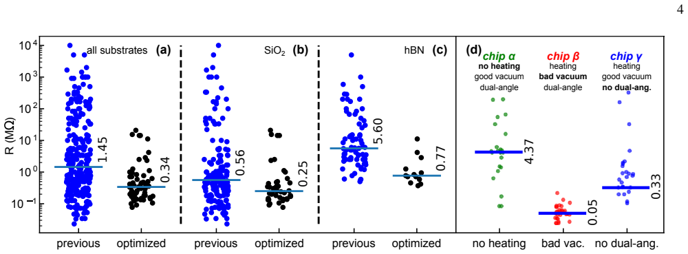
Bismuth contacts to MoS2 nanotubes and nanoribbons achieve reproducible finite room-temperature two-point resistances with a median of 340 kΩ.
A machine-rendered reading of the paper's core claim, the machinery that carries it, and where it could break.
Core claim
Using bismuth semimetal contacts together with targeted fabrication process adjustments makes it possible to produce contacts to individual MoS2 nanotubes and nanoribbons that consistently show finite two-point resistances at room temperature in the absence of gating, reaching a median value of 340 kΩ across a large fabrication series.
What carries the argument
Bismuth semimetal contacts applied through optimized fabrication steps to vapor-phase grown MoS2 nanotubes and nanoribbons.
If this is right
- Contact resistances no longer scatter widely on the same chip for these curved nanostructures.
- MoS2 nanotubes and nanoribbons become more viable as building blocks for field-effect transistors.
- Quantum electronic devices based on these materials gain a practical route to metallic leads.
- The same bismuth-based approach used for flat MoS2 flakes can be adapted to tubular and ribbon geometries.
- Analysis of individual fabrication steps isolates which changes most improve contact performance.
Where Pith is reading between the lines
- The method may extend to other curved transition-metal dichalcogenide structures where contact formation has been difficult.
- Reproducible contacts could enable systematic studies of transport properties that were previously limited by contact variability.
- If nanotube diameter or chirality variations remain uncontrolled, further process tuning may still be needed for even tighter resistance distributions.
Load-bearing premise
The specific fabrication process changes are what produce the observed reproducibility rather than uncontrolled differences in nanotube quality or measurement setup.
What would settle it
A replication attempt that applies the reported fabrication steps but still produces wide scatter in contact resistances across devices on the same chip would falsify the claim.
Figures
read the original abstract
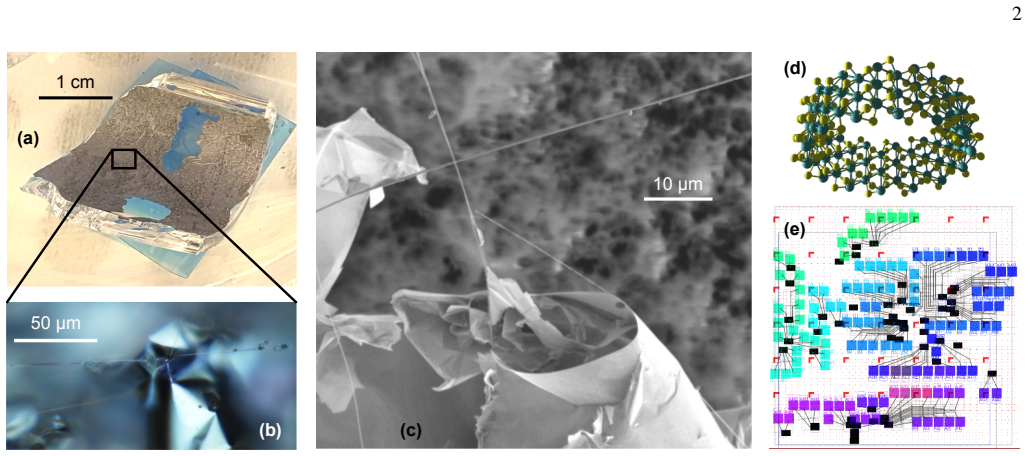
Attaching metallic contacts to transition metal dichalcogenide nanostructures and in particular to $\textrm{MoS}_2$ has posed significant challenges over the past years. For $\textrm{MoS}_2$ nanotubes and nanoribbons, a highly promising material for field effect transistors as well as quantum electronic devices, this is even more the case due to the small, curved surface. So far all attempts there have led to a wide scatter of contact resistances on the same chip. Recently, for quasi two-dimensional, flat $\textrm{MoS}_2$ flakes, the use of semimetals has led to a breakthrough, making transparent and Ohmic contacts possible. Here, we demonstrate the steps required to reproducibly fabricate contacts to single, vapor phase grown $\textrm{MoS}_2$ nanotubes and nanowires. All devices display finite room-temperature two-point resistances in absence of gating, with a median value of $340\,\textrm{k}\Omega$ in a large fabrication series. A detailed analysis elucidates the impact of the different fabrication changes.
Editorial analysis
A structured set of objections, weighed in public.
Referee Report
Summary. The manuscript presents a fabrication process for bismuth contacts to vapor-phase grown MoS₂ nanotubes and nanoribbons that yields reproducible Ohmic behavior. All devices in a large series exhibit finite room-temperature two-point resistances without gating, with a reported median value of 340 kΩ; the authors provide a detailed analysis attributing the improvement to specific changes in the contact fabrication sequence relative to prior attempts that showed wide scatter.
Significance. If the attribution to the bismuth process holds after controls, the result would be significant for enabling reliable transport measurements and device applications in 1D TMD nanostructures, extending the semimetal-contact approach recently successful on flat 2D MoS₂ flakes. The work directly addresses a long-standing experimental bottleneck in the field.
major comments (2)
- [Results / Fabrication analysis] Results section (or equivalent): the central claim that the observed consistency (all finite resistances, median 340 kΩ) arises from the bismuth-contact fabrication changes rather than from uncontrolled variations in nanotube quality requires explicit controls. No pre-contact characterization (TEM, Raman, or ungated metrics on the same nanotubes) or same-batch comparisons between old and new processes are described; without these, the reduced scatter could reflect growth-batch selection effects.
- [Abstract and Results] The abstract states that all devices conducted and supplies a median resistance, but the manuscript must include raw I-V curves, device-by-device resistances with error bars or histograms, and confirmation that the contacts are linear (Ohmic) rather than merely finite. These data are load-bearing for the reproducibility claim.
minor comments (2)
- [Figures and Methods] Figure captions and methods should explicitly state the number of devices measured, the range of nanotube diameters, and any post-fabrication annealing or gating conditions used for the two-point data.
- [Introduction] The manuscript should cite the specific prior works on MoS₂ nanotube contacts that showed scatter, to allow direct comparison of the new median value.
Simulated Author's Rebuttal
We thank the referee for the positive assessment of significance and for the constructive major comments. We address each point below and will revise the manuscript to strengthen the presentation of the reproducibility claim.
read point-by-point responses
-
Referee: [Results / Fabrication analysis] Results section (or equivalent): the central claim that the observed consistency (all finite resistances, median 340 kΩ) arises from the bismuth-contact fabrication changes rather than from uncontrolled variations in nanotube quality requires explicit controls. No pre-contact characterization (TEM, Raman, or ungated metrics on the same nanotubes) or same-batch comparisons between old and new processes are described; without these, the reduced scatter could reflect growth-batch selection effects.
Authors: We agree that pre-contact characterization of the same nanotubes and same-batch comparisons would provide the strongest possible isolation of the fabrication-sequence effect. The current manuscript attributes the improvement to the specific changes in contact fabrication by direct comparison with the authors' prior attempts on similar vapor-phase material that exhibited wide scatter; the large series (all devices finite) is presented as evidence that the new sequence produces consistent results. We will revise the Results section to add an explicit limitations paragraph acknowledging the absence of pre-contact TEM/Raman on the contacted tubes and the lack of same-batch old-vs-new controls, and to clarify that growth-batch selection cannot be fully ruled out. If any supporting growth metrics exist in the authors' records they will be included; otherwise the attribution will be presented with the appropriate caveat. revision: partial
-
Referee: [Abstract and Results] The abstract states that all devices conducted and supplies a median resistance, but the manuscript must include raw I-V curves, device-by-device resistances with error bars or histograms, and confirmation that the contacts are linear (Ohmic) rather than merely finite. These data are load-bearing for the reproducibility claim.
Authors: We will add the requested data to the revised manuscript. A new figure (or expanded Results subsection) will show representative raw I-V curves for multiple devices, a histogram of all two-point resistances, and a statement confirming linearity within the measured bias range. Device-by-device values with any available uncertainty will be tabulated or plotted. These additions directly support the abstract claim and the reproducibility statement. revision: yes
Circularity Check
No circularity: purely experimental report with no derivations or fitted predictions
full rationale
The manuscript is an experimental fabrication study reporting measured two-point resistances (median 340 kΩ) across devices. No equations, first-principles derivations, parameter fits, or 'predictions' appear anywhere in the text. The central claim rests on direct electrical measurements from a fabrication series rather than any reduction to self-defined inputs or self-citations. External controls and nanotube characterization are separate validity questions, not circularity. This matches the default expectation of score 0 for self-contained experimental work.
Axiom & Free-Parameter Ledger
Reference graph
Works this paper leans on
-
[1]
Spot anchoring
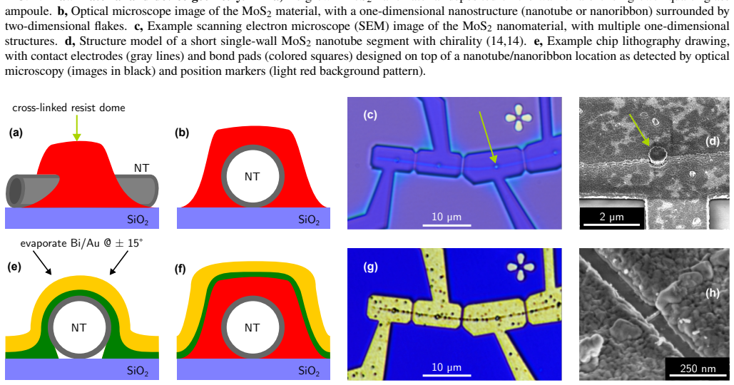
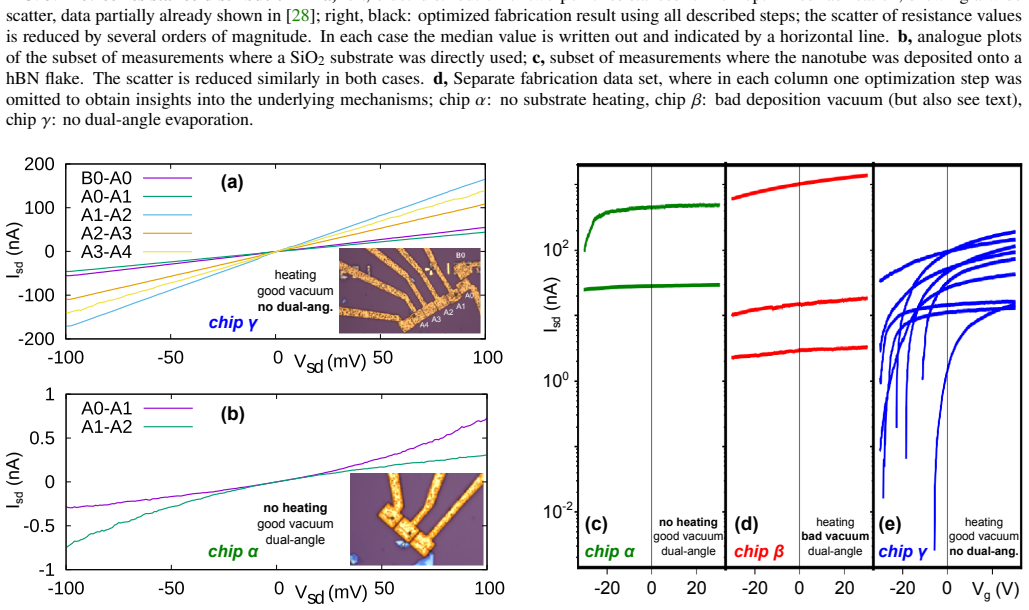
Predominantly, linear behaviour was observed, see, e.g., the measurement of several nanotube segments on chip𝛾in Fig. 4(a). The only occurences of clear diode-like response were on chip𝛼, where the substrate was not heated during contact deposition. This is demonstrated in Fig. 4(b) with the response of two neighboring segments; the curves nearly coincide...
-
[2]
Novoselov, K. S.et al.Electric field effect in atomically thin carbon films.Science306, 666–669 (2004). URLhttps: //www.science.org/doi/10.1126/science.1102896
work page internal anchor Pith review doi:10.1126/science.1102896 2004
-
[3]
S.et al.Two-dimensional atomic crystals.Pro- ceedings of the National Academy of Sciences102, 10451– 10453 (2005)
Novoselov, K. S.et al.Two-dimensional atomic crystals.Pro- ceedings of the National Academy of Sciences102, 10451– 10453 (2005). URLhttps://www.pnas.org/content/ 102/30/10451
2005
-
[4]
URLhttps://www.nature.com/articles/ s41928-021-00670-1
Das, S.et al.Transistors based on two-dimensional materi- als for future integrated circuits.Nature Electronics4, 786– 799 (2021). URLhttps://www.nature.com/articles/ s41928-021-00670-1
2021
-
[5]
Dorow, C. J.et al.Exploring manufacturability of novel 2D channel materials: 300mm wafer-scale 2D NMOS & PMOS using MoS 2, WS 2, & WSe 2. In2023 International Electron Devices Meeting (IEDM), 1–4 (2023). URLhttps://dx.doi. org/10.1109/IEDM45741.2023.10413874
-
[6]
Chou, A.-S.et al.Status and performance of integration modules toward scaled CMOS with transition metal dichalco- genide channel. In2023 International Electron Devices Meeting (IEDM), 1–4 (2023). URLhttps://dx.doi.org/10.1109/ IEDM45741.2023.10413779
-
[7]
URLhttps://dx.doi.org/10.1002/qute.202100162
Jing, F.-M.et al.Gate-controlled quantum dots based on 2D materials.Advanced Quantum Technologies5, 2100162 (2022). URLhttps://dx.doi.org/10.1002/qute.202100162
-
[8]
& Hersam, M
Liu, X. & Hersam, M. C. 2D materials for quantum information science.Nature Reviews Materials4, 669– 684 (2019). URLhttps://www.nature.com/articles/ s41578-019-0136-x
2019
-
[9]
URLhttps://onlinelibrary.wiley.com/doi/abs/10
Qiu, D.et al.Recent advances in 2D supercon- ductors.Advanced Materials33, 2006124 (2021). URLhttps://onlinelibrary.wiley.com/doi/abs/10. 1002/adma.202006124
2021
-
[10]
URLhttps://www.nature.com/articles/ s41586-019-1493-8
Hills, G.et al.Modern microprocessor built from com- plementary carbon nanotube transistors.Nature572, 595– 602 (2019). URLhttps://www.nature.com/articles/ s41586-019-1493-8
2019
-
[11]
Nature Electronics7, 684–693 (2024)
Si, J.et al.A carbon-nanotube-based tensor processing unit. Nature Electronics7, 684–693 (2024). URLhttps://www. nature.com/articles/s41928-024-01211-2
2024
-
[12]
Stern, A. & Lindner, N. H. Topological quantum computa- tion—from basic concepts to first experiments.Science339, 1179–1184 (2013). URLhttps://www.science.org/doi/ 10.1126/science.1231473
-
[13]
Frolov, S. M.et al.Data sharing helps avoid “smoking gun” claims of topological milestones.Science391, 137– 142 (2026). URLhttps://www.science.org/doi/abs/ 10.1126/science.adk9181
-
[14]
Xiang, R.et al.One-dimensional van der Waals heterostruc- tures.Science367, 537–542 (2020). URLhttps://www. science.org/doi/10.1126/science.aaz2570
-
[15]
Remskar, M., Skraba, Z., Cl ´eton, F., Sanjin ´es, R. & L ´evy, F. MoS2 as microtubes.Appl. Phys. Lett.69, 351–353 (1996). 7 URLhttps://dx.doi.org/10.1063/1.118057
-
[16]
R.et al.Multiwall MoS2 tubes as optical resonators
Kazanov, D. R.et al.Multiwall MoS2 tubes as optical resonators. Applied Physics Letters113, 101106 (2018). URLhttps: //dx.doi.org/10.1063/1.5047792
-
[17]
Remskar, M.et al.Confinement related phenomena in MoS 2 tubular structures grown from vapour phase.Israel Journal of Chemistry62, e202100100 (2022). URLhttps://dx.doi. org/10.1002/ijch.202100100
-
[18]
Fathipour, S.et al.Synthesized multiwall MoS 2 nanotube and nanoribbon field-effect transistors.Appl. Phys. Lett.106, 022114 (2015). URLhttps://dx.doi.org/10.1063/1.4906066
-
[19]
Schottky, W. Zur Halbleitertheorie der Sperrschicht- und Spitzengleichrichter.Zeitschrift f ¨ur Physik113, 367–414 (1939). URLhttps://dx.doi.org/10.1007/BF01340116
-
[20]
Tung, R. T. The physics and chemistry of the Schottky bar- rier height.Applied Physics Reviews1, 011304 (2014). URL https://aip.scitation.org/doi/10.1063/1.4858400
-
[21]
Louie, S. G. & Cohen, M. L. Electronic structure of a metal- semiconductor interface.Physical Review B13, 2461–2469 (1976). URLhttps://dx.doi.org/10.1103/PhysRevB. 13.2461
-
[22]
M ¨onch, W. Valence-band offsets and Schottky barrier heights of layered semiconductors explained by interface-induced gap states.Applied Physics Letters72, 1899–1901 (1998). URL https://dx.doi.org/10.1063/1.121220
-
[23]
Gong, C., Colombo, L., Wallace, R. M. & Cho, K. The un- usual mechanism of partial Fermi level pinning at metal–MoS2 interfaces.Nano Letters14, 1714–1720 (2014). URLhttps: //dx.doi.org/10.1021/nl403465v
-
[24]
URLhttps://dx.doi.org/10.1021/ acsnano.6b07159
Kim, C.et al.Fermi level pinning at electrical metal contacts of monolayer molybdenum dichalcogenides.ACS Nano11, 1588–1596 (2017). URLhttps://dx.doi.org/10.1021/ acsnano.6b07159
2017
-
[25]
URLhttps://dx.doi.org/10
Sotthewes, K.et al.Universal Fermi-level pinning in transition- metal dichalcogenides.The Journal of Physical Chemistry C123, 5411–5420 (2019). URLhttps://dx.doi.org/10. 1021/acs.jpcc.8b10971
2019
-
[26]
URLhttps://dx.doi.org/10.1038/ s41586-021-03472-9
Shen, P.-C.et al.Ultralow contact resistance between semimetal and monolayer semiconductors.Nature593, 211–217 (2021). URLhttps://dx.doi.org/10.1038/ s41586-021-03472-9
2021
-
[27]
Schock, R. T. K.et al.Non-destructive low-temperature contacts to MoS 2 nanoribbon and nanotube quantum dots.Advanced Materials35, 2209333 (2023). URLhttps://dx.doi.org/ 10.1002/adma.202209333
-
[28]
URL https://dx.doi.org/10.1038/s41586-022-05431-4
Li, W.et al.Approaching the quantum limit in two-dimensional semiconductor contacts.Nature613, 274–279 (2023). URL https://dx.doi.org/10.1038/s41586-022-05431-4
-
[29]
Schock, R. T. K.et al.Material transfer and contact op- timization in MoS 2 nanotube devices.physica status solidi (b)262, 2400366 (2025). URLhttps://onlinelibrary. wiley.com/doi/abs/10.1002/pssb.202400366
-
[30]
Zailer, I., Frost, J. E. F., Chabasseur-Molyneux, V., Ford, C. J. B. & Pepper, M. Crosslinked PMMA as a high-resolution negative resist for electron beam lithography and applications for physics of low-dimensional structures.Semiconductor Science and Technology11, 1235 (1996). URLhttps://dx.doi.org/ 10.1088/0268-1242/11/8/021
-
[31]
Jarillo-Herrero, P., Sapmaz, S., Dekker, C., Kouwenhoven, L. P. & van der Zant, H. S. J. Electron-hole symmetry in a semi- conducting carbon nanotube quantum dot.Nature429, 389– 392 (2004). URLhttps://www.nature.com/articles/ nature02568
2004
-
[32]
URLhttps://www
Jarillo-Herrero, P.et al.Orbital Kondo effect in carbon nan- otubes.Nature434, 484–488 (2005). URLhttps://www. nature.com/articles/nature03422
2005
-
[33]
Jarillo-Herrero, P. (2007). Private communication
2007
-
[34]
ACS Nano18, 22444–22453 (2024)
Sun, Z.et al.Low contact resistance on monolayer MoS 2 field- effect transistors achieved by CMOS-compatible metal contacts. ACS Nano18, 22444–22453 (2024). URLhttps://dx.doi. org/10.1021/acsnano.4c07267
-
[35]
Das, S., Chen, H.-Y., Penumatcha, A. V. & Appenzeller, J. High performance multilayer MoS 2 transistors with scandium contacts.Nano Letters13, 100–105 (2013). URLhttps: //dx.doi.org/10.1021/nl303583v
-
[36]
& H¨ uttel, A
Reinhardt, S., Pirker, L., B ¨auml, C., Rem ˇskar, M. & H¨ uttel, A. K. Coulomb blockade spectroscopy of a MoS 2 nan- otube.physica status solidi (RRL) – Rapid Research Letters 13, 1900251 (2019). URLhttps://dx.doi.org/10.1002/ pssr.201900251
2019
-
[37]
Wu, R. J.et al.Visualizing the metal-MoS 2 contacts in two- dimensional field-effect transistors with atomic resolution.Phys. Rev. Materials3, 111001 (2019). URLhttps://dx.doi.org/ 10.1103/PhysRevMaterials.3.111001
-
[38]
In2018 IEEE 13th Nanotechnology Mate- rials and Devices Conference, 1–4 (IEEE, Portland, OR, USA, 2018)
Liu, M.et al.Improvement of metal-semiconductor contact from Schottky to Ohmic by Cu doping in transition metal dichalco- genide transistors. In2018 IEEE 13th Nanotechnology Mate- rials and Devices Conference, 1–4 (IEEE, Portland, OR, USA, 2018). URLhttps://ieeexplore.ieee.org/document/ 8605891/
2018
-
[39]
URLhttps: //www.nature.com/articles/s41928-024-01176-2
Jiang, J.et al.Yttrium-doping-induced metallization of molyb- denum disulfide for Ohmic contacts in two-dimensional tran- sistors.Nature Electronics7, 545–556 (2024). URLhttps: //www.nature.com/articles/s41928-024-01176-2
2024
-
[40]
Lizzit, D., Khakbaz, P., Driussi, F., Pala, M. & Esseni, D. Ohmic behavior in metal contacts to n/p-type transition-metal dichalcogenides: Schottky versus tunneling barrier trade-off. ACS Applied Nano Materials(2023). URLhttps://doi.org/ 10.1021/acsanm.3c00166
-
[41]
URLhttps://dx.doi.org/10.1063/5.0155663
Chen, Y.et al.Gate-tunable superconductivity in hybrid InSb–Pb nanowires.Applied Physics Letters123, 082601 (2023). URLhttps://dx.doi.org/10.1063/5.0155663
-
[42]
URL https://dx.doi.org/10.1016/j.apsusc.2006.12.125
Kumari, L.et al.Effects of deposition temperature and thickness on the structural properties of thermal evaporated bismuth thin films.Applied Surface Science253, 5931–5938 (2007). URL https://dx.doi.org/10.1016/j.apsusc.2006.12.125
-
[43]
Partin, D. L., Thrush, C. M., Heremans, J., Morelli, D. T. & Olk, C. H. Growth and characterization of epitaxial bismuth films. Journal of Vacuum Science & Technology B: Microelectronics Processing and Phenomena7, 348–353 (1989). URLhttps: //doi.org/10.1116/1.584748
-
[44]
Li, L.-J. (2024). Private communication
2024
-
[45]
Okamoto, H. & Massalski, T. B. The Au-Bi (gold-bismuth) system.Bulletin of Alloy Phase Diagrams4, 401–407 (1983). URLhttps://dx.doi.org/10.1007/BF02868093
-
[46]
de Haas, W. J. & Jurriaanse, F. The super-conductivity of gold- bismuth.Naturwissenschaften19, 706–706 (1931)
1931
-
[47]
McDonnell, S., Addou, R., Buie, C., Wallace, R. M. & Hinkle, C. L. Defect-dominated doping and contact resistance in MoS2. ACS Nano8, 2880–2888 (2014). URLhttps://dx.doi.org/ 10.1021/nn500044q
-
[48]
URLhttps: //www.nature.com/articles/s41557-018-0136-2
Pet ˝o, J.et al.Spontaneous doping of the basal plane of MoS 2 single layers through oxygen substitution under ambient condi- tions.Nature Chemistry10, 1246–1251 (2018). URLhttps: //www.nature.com/articles/s41557-018-0136-2
2018
-
[49]
npj 2D Materials and Applications7, 1–9 (2023)
Schwarz, A.et al.Thiol-based defect healing of WSe 2 and WS2. npj 2D Materials and Applications7, 1–9 (2023). URLhttps: 8 //www.nature.com/articles/s41699-023-00421-0
2023
-
[50]
Malok, M., Jelenc, J., Krajnc, A. P. & Rem ˇskar, M. Edge and defect effects on charge distribution in collapsed MoS 2 nanotubes.Nanoscale Advances7, 8161–8169 (2025). URL https://dx.doi.org/10.1039/D5NA00771B
-
[51]
Malok, M., Jelenc, J. & Rem ˇskar, M. Electrical properties of collapsed MoS 2 nanotubes.Nanoscale17, 12361–12370 (2025). URLhttps://dx.doi.org/10.1039/D5NR00284B
-
[52]
Khadiev, A.et al.Misfit layered compounds: Insights into chemical, kinetic, and thermodynamic stability of nanophases.Accounts of Chemical Research57, 3243–3253 (2024). URLhttps://pubs.acs.org/doi/10.1021/acs. accounts.4c00412
work page doi:10.1021/acs 2024
-
[53]
URLhttps://dx.doi.org/10.1016/j.cpc
Reinhardt, S.et al.Lab::Measurement — a portable and ex- tensible framework for controlling lab equipment and conduct- ing measurements.Computer Physics Communications234, 216 (2019). URLhttps://dx.doi.org/10.1016/j.cpc. 2018.07.024
discussion (0)
Sign in with ORCID, Apple, or X to comment. Anyone can read and Pith papers without signing in.