REVIEW 2 major objections 4 minor 46 references
Emission dynamics in zincblende InAsxP1-x quantum dots in InP nanowires: influence of quantum dot size, composition and nanowire geometry
T0 review · 2 major / 4 minor · reviewed 2026-08-15 · deepseek-v4-flash
Pith's one-line read Exciton lifetimes in InAsP/InP nanowire dots are governed jointly by dot height, arsenic content, and shell thickness.
desk verdict First systematic lifetime data for zincblende InAsP/InP QD-NWs, with honest modeling—but the Purcell inhibition claim is quantitatively loose. read the letter →
The pith
A machine-rendered reading of the paper's core claim, the machinery that carries it, and where it could break.
The reading
What carries the argument
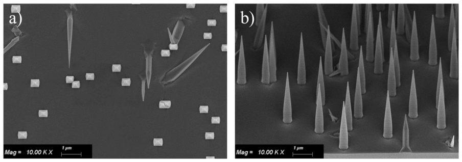
The argument is carried by pairing two computational tools with structural input. The electronic part uses an eight-band k·p band-structure calculation with a configuration-interaction basis of the twenty lowest electron and hole states to compute exciton energies, oscillator strengths, and radiative lifetimes as functions of dot height and arsenic composition; these calculations show that Coulomb correlations significantly shorten the lifetime and that taller dots have larger electron-hole overlap. The photonic part uses finite-difference time-domain simulations of an InP nanowire with a point dipole to compute the Purcell factor, the factor by which the photonic environment multiplies or suppresses the spontaneous emission rate, as a function of shell width and emission wavelength. This identifies the single-mode waveguide regime near a width-to-wavelength ratio of about 0.20 to 0.31 and the inhibited regime below it. The structural parameters that feed both models come from high-resolution electron microscopy and energy-dispersive X-ray spectroscopy. The central comparison is the product of these two mechanisms: the dot potential fixes the bare radiative lifetime, and the shell thickness multiplies it through the Purcell effect.
What would settle it
Measure time-resolved photoluminescence on single nanowires containing nominally identical dots: one with a 55 nm shell and one with a 150 nm shell, at excitation low enough to isolate the neutral exciton. If the thin-shell single-dot lifetime is not roughly an order of magnitude longer, the paper's quantitative claim about spontaneous-emission inhibition would be unsupported; if the ratio remains near two even for single dots, the ensemble-averaging explanation would be wrong.
Extended reading notes
Core claim
On its own terms, the paper establishes that no single mechanism accounts for the measured emission dynamics in zincblende InAsP/InP quantum-dot nanowires. The full explanation requires both the quantum-dot potential and the photonic environment: the dot height and arsenic composition set the electron-hole overlap and exciton oscillator strength, while the InP shell thickness sets the Purcell factor by determining whether the nanowire confines the fundamental HE11 guided mode. Quantitative support comes from comparing three samples: a 10 nm dot with a 150 nm shell decays in about 1.8 ns; a 2 nm dot with a 150 nm shell decays in about 1.35 ns; and a 2 nm dot with a 55 nm shell decays in about 2.8 ns. The thin-shell sample, whose dot is nominally identical to the 150 nm-shell 2 nm dot, shows the signature of spontaneous-emission inhibition, although the measured factor of two is smaller than the factor of ten predicted for a single dot because the measurement averages over thousands of wires, excited states, and excitonic complexes.
Load-bearing premise
The quantitative match between model and data assumes that a single-exponential fit to an ensemble photoluminescence decay represents the ground-state exciton radiative lifetime of one modelled dot, even though the signal averages thousands of nanowires with a spread of dot sizes, compositions, and excitation conditions; the paper identifies this averaging as the reason the predicted ten-fold inhibition appears only as two-fold.
Editorial extensions
If this is right
- If the central claim is right, zincblende InAsP/InP quantum-dot nanowires with thick shells offer radiative lifetimes of 1.1 to 1.8 ns across the 1100 to 1600 nm range, shorter than the >2 ns lifetimes reported for wurtzite telecom nanowire dots, which is favorable for faster single-photon emission.
- Dot height and arsenic composition can be used as independent design levers for the lifetime: a 2-to-10 nm height increase outweighs a few-percent change in arsenic content.
- A 55 nm InP shell is below the cutoff for the fundamental guided mode and should inhibit spontaneous emission by up to an order of magnitude for a single dot; the ensemble measurement gives a lower bound of about a factor of two.
- The thick-shell geometry keeps the Purcell factor above 0.8 across the measured spectral range, so lifetime differences between the two thick-shell samples remain small despite different emission wavelengths.
- Because the measured decay curves are monoexponential and the calculated lifetimes match, non-radiative recombination is not required to explain the short decay times.
Reading between the lines
- Editorial inference: if single-dot measurements reproduce the predicted order-of-magnitude inhibition, shell thickness becomes a growth-independent knob for lifetime engineering in this platform, allowing faster photon sources without changing the dot itself.
- Editorial inference: the same ensemble-averaging bias likely affects other time-resolved studies of nanowire quantum-dot ensembles; comparing single-dot and ensemble lifetimes would give a direct estimate of the width of the dot parameter distribution and the contribution of charged or excited states.
- Editorial inference: because the arsenic content changes carrier effective masses as well as the band gap, it may be possible to tune emission wavelength while partially decoupling it from lifetime by choosing dot heights that compensate the mass effect.
Signed reviews
Editorial analysis
A structured set of objections, weighed in public.
Referee Report
Summary. This manuscript combines structural characterization (SEM/STEM/EDS), eight-band k.p modeling with configuration-interaction exciton calculations, FDTD photonic simulations, and time-resolved photoluminescence to study exciton lifetimes in zincblende InAsP/InP quantum-dot nanowires grown by CBE-VLS. Three samples are compared: 10-nm QDs with a 150-nm InP shell, 2-nm QDs with a 55-nm shell, and 2-nm QDs with a 150-nm shell. Measured ensemble average lifetimes are about 1.8 ns, 2.8 ns, and 1.35 ns, respectively. The paper shows that the lifetime trends with QD height and As composition follow from the calculated ground-state exciton properties, and it attributes the longer lifetime of the thin-shell sample to Purcell inhibition, although the measured ratio is only about a factor of two rather than the predicted roughly tenfold; the authors ascribe this discrepancy to ensemble averaging and excited-state contributions.
Significance. If the quantitative Purcell claim could be substantiated, the paper would provide useful design rules for controlling emission dynamics in telecom-wavelength zincblende InAsP/InP QD-NWs and a methodological template combining structural characterization, k.p-CI exciton calculations, and FDTD photonic simulations. The qualitative trends (lifetime increasing with QD height and As content, thin shell elongating lifetime) are credible and consistent with independent literature. Notable strengths are that the calculated lifetimes are not fitted to the measured decays, the structural inputs come from independent TEM/EDS data, and the model includes strain, piezoelectric fields, Coulomb correlations, alloy intermixing, and the photonic environment. The main weakness is that the central quantitative inference about Purcell inhibition is not yet strictly supported by the ensemble measurements.
major comments (2)
- [Section 3.4, Fig. 7(d)] The quantitative Purcell-inhibition claim is not yet established. The measured ensemble TRPL is fitted mono-exponentially and compared with a calculated single-QD ground-state lifetime, but Sections 3.4 and 4 themselves state that the ensemble includes thousands of QD-NWs with a spread of parameters and contributions from shorter-lived excitonic complexes and excited states, and that sample B required a higher excitation power (55 µW vs 25 µW) that biases its decay toward short-lived states. Under the FDTD model of Fig. 6(a), sample B (d ≈ 160 nm, λ ≈ 1120 nm, d/λ ≈ 0.143) should show a lifetime at least about ten times longer than sample C, whereas the measured ratio is 2.8/1.35 ≈ 2.1. Without a quantitative model of the ensemble-averaging correction, the same data are equally consistent with a much weaker Purcell effect or with uncharacterized QD differences between samples B and C, whose PL peaks differ by about 55 nm; the statement in Section 3.4 that the increase is qualitatively in agreement with the photonic calculations is appropriate, but the abstract's stronger conclusion that full understanding requires the Purcell effect needs further support.
- [Section 3.4, Fig. 7(a-d)] The averaged lifetimes are reported without uncertainties, error bars, or confidence intervals, and without the number of independent measurements or nanowires contributing to each value. Because the 2.1-fold B/C ratio is the sole experimental evidence for the Purcell-inhibition claim, the spread of decay-time values visible in Fig. 7(a-c) needs to be quantified to show that this ratio is statistically meaningful rather than reflecting collection-spot or sample heterogeneity.
minor comments (4)
- [Section 3.2] The scaling of the lifetime with exciton energy is stated once as τ ∝ 1/E_n and later as τ ∝ 1/E_n^2; Eq. (2) and the text should be made mutually consistent.
- [Section 3.3] The phrase 'at last 10-fold increase' should read 'at least 10-fold increase'.
- [Section 2.2] The name 'Feynmann-Hellman theorem' should be spelled 'Feynman-Hellman theorem'.
- [Section 3.4, Fig. 7(d)] The inset values tA = 1.75 ns, tB = 2.86 ns, and tC = 1.35 ns differ slightly from the text averages of about 1.8, 2.8, and 1.35 ns; clarify whether the inset shows representative single-decay fits or sample averages.
Circularity Check
No significant circularity: the calculated lifetimes are derived from independent k.p/CI and FDTD simulations with measured structural inputs, and the measured lifetimes are not used as fitting parameters.
full rationale
The paper's central derivation chain is self-contained against external inputs. The QD electronic structure is computed with an eight-band k.p model whose material parameters come from published tight-binding and band-structure fits (Jancu et al., Vurgaftman et al.), and the exciton states are obtained by configuration interaction. The QD geometry, size, and composition are taken from HRSTEM/EDS measurements of the grown structures rather than from the optical decay data. The Purcell factor is computed by FDTD using SEM-determined NW dimensions, an independently measured emission wavelength range, and a point-dipole model; no parameter is fitted to the measured TRPL lifetimes. The measured PL decays are then compared with the predicted lifetimes only after the calculation, and the paper explicitly acknowledges the deviations (e.g., the predicted ten-fold Purcell inhibition appears as only a two-fold effect in Section 3.4, attributed to ensemble averaging and stronger excitation for sample B). While this ensemble-to-single-QD comparison is a methodological limitation, it is not a circular reduction: no equation of the paper defines a prediction in terms of the measured lifetimes, and no load-bearing step reduces to a self-citation. The only self-citations concern growth methodology and prior demonstrations of tunable ZB QD-NW emission, which are not the basis of the theoretical lifetime derivation.
Assumptions & free parameters
free parameters (4)
- cmin/cmax ratio =
0.75
- Lateral composition spread σr =
15 nm
- Axial composition spread σz =
sqrt(2/3)*h
- Gaussian intermixing blur =
0.6 nm
assumptions (5)
- domain assumption Eight-band k·p model with material parameters from Jancu et al. and Vurgaftman et al. accurately describes the electronic structure of InAsP/InP QDs.
- domain assumption Continuous elasticity with second-order piezoelectricity gives the correct strain field in the QD.
- domain assumption The CI model truncated to the 20 lowest electron and hole states captures the exciton ground state oscillator strength.
- domain assumption The ensemble TRPL decay fitted by a single exponential represents the ground-state exciton radiative lifetime.
- domain assumption The FDTD model treating the QD as a point dipole at the nanowire center captures the Purcell factor for the actual extended QD.
Cite this review
Pith. "Pith review of Emission dynamics in zincblende InAsxP1-x quantum dots in InP nanowires: influence of quantum dot size, composition and nanowire geometry." pith.science (2026). https://pith.science/paper/HFJAZJS4
@misc{pith2026260802029,
  author       = {Pith},
  title        = {Pith review of: Emission dynamics in zincblende InAsxP1-x quantum dots in InP nanowires: influence of quantum dot size, composition and nanowire geometry},
  year         = {2026},
  howpublished = {\url{https://pith.science/paper/HFJAZJS4}},
  note         = {Machine review of arXiv:2608.02029}
}
read the original abstract
Hereby, we present an experimental and theoretical investigation of emission dynamics in zincblende InAsxP1-x quantum dots (QDs) embedded in InP nanowires (NWs) grown via vapour-liquid-solid mechanism by chemical beam epitaxy, using Au nanoparticles as a nucleation catalyst. By measuring time-resolved photoluminescence from an ensemble of QD-NWs it was possible to determine the exciton lifetime dependence on QD composition and height. Changes in the InP shell thickness surrounding the InP NW stem with a QD, brought additional insight into the influence of photonic environment on the carrier dynamics. High-resolution transmission electron microscopy, combined with energy-dispersive X-ray spectroscopy, provided actual structural parameters. The experimentally obtained lifetimes were interpreted in the light of results of 8 band kp calculations combined with configuration-interaction model to take into account the Coulomb interactions and finite-difference time domain photonic simulations to include the effect of optical confinement. The full understanding of the experimental results required considering both, the changes in the QD potential and the Purcell effect, the latter leading to spontaneous emission inhibition in the case of NWs with thin InP shell.
Figures


Figures from the paper (2 more)


Reference graph
Works this paper leans on
-
[1]
A. Kiraz, M. Atatüre, and A. Imamoǧlu, “Quantum-dot single-photon sources: Prospects for applications in linear optics quantum-information processing,” Phys. Rev. A, vol. 69, no. 3, 2004, doi: 10.1103/PhysRevA.69.032305
-
[2]
H. J. Kimble, “The quantum internet,” Nature, vol. 453, no. 7198, pp. 1023–1030, Jun. 2008, doi: 10.1038/nature07127
-
[3]
Quantum Communication Using Semiconductor Quantum Dots,
D. A. Vajner, L. Rickert, T. Gao, K. Kaymazlar, and T. Heindel, “Quantum Communication Using Semiconductor Quantum Dots,” Jul. 01, 2022, John Wiley and Sons Inc. doi: 10.1002/qute.202100116
-
[4]
Quantum Repeaters: The Role of Imperfect Local Operations in Quantum Communication,
H.-J. Briegel, W. Dür, J. I. Cirac, and P. Zoller, “Quantum Repeaters: The Role of Imperfect Local Operations in Quantum Communication,” 1998
work page 1998
-
[5]
Time-bin encoded quantum key distribution over 120 km with a telecom quantum dot source,
J. Wang et al., “Time-bin encoded quantum key distribution over 120 km with a telecom quantum dot source,” Aug. 2025, doi: 10.1038/s41377-026-02205-9
-
[6]
High-rate intercity quantum key distribution with a semiconductor single-photon source,
J. Yang et al., “High-rate intercity quantum key distribution with a semiconductor single-photon source,” Light Sci. Appl., vol. 13, no. 1, Dec. 2024, doi: 10.1038/s41377-024-01488-0
-
[7]
Quantum key distribution using deterministic single-photon sources over a field-installed fibre link,
M. Zahidy et al., “Quantum key distribution using deterministic single-photon sources over a field-installed fibre link,” npj Quantum Inf., vol. 10, no. 1, Dec. 2024, doi: 10.1038/s41534-023-00800-x
-
[8]
Single-emitter quantum key distribution over 175 km of fibre with optimised finite key rates,
C. L. Morrison et al., “Single-emitter quantum key distribution over 175 km of fibre with optimised finite key rates,” Nat. Commun., vol. 14, no. 1, Dec. 2023, doi: 10.1038/s41467-023-39219-5
Show all 46 references
-
[9]
Engineering Nanohole-Etched Quantum Dots for Telecom- Band Single-Photon Generation,
I. M. Masson et al., “Engineering Nanohole-Etched Quantum Dots for Telecom- Band Single-Photon Generation,” ACS Nano, vol. 3, no. 20, pp. 2872–2880, Jan. 2026, doi: 10.1021/acsnano.5c17982
2026 doi
- [10]
-
[11]
Springer Cham, 2017
Michler Peter, Nano-Optics and Nanophotonics, 1st ed. Springer Cham, 2017. doi: 10.1007/978-3-319-56378-7
2017 doi
-
[12]
Crystal phase quantum dots,
N. Akopian, G. Patriarche, L. Liu, J. C. Harmand, and V. Zwiller, “Crystal phase quantum dots,” Nano Lett., vol. 10, no. 4, pp. 1198–1201, Apr. 2010, doi: 10.1021/nl903534n
2010 doi
-
[13]
Ultraclean emission from InAsP quantum dots in defect-free wurtzite InP nanowires,
D. Dalacu et al., “Ultraclean emission from InAsP quantum dots in defect-free wurtzite InP nanowires,” Nano Lett., vol. 12, no. 11, pp. 5919–5923, Nov. 2012, doi: 10.1021/nl303327h
2012 doi
-
[14]
Bright single-photon sources in bottom-up tailored nanowires,
M. E. Reimer et al., “Bright single-photon sources in bottom-up tailored nanowires,” Nat. Commun., vol. 3, no. 737, 2012, doi: 10.1038/ncomms1746
2012 doi
-
[15]
Solid-state single photon sources: the nanowire antenna,
I. Friedler, C. Sauvan, J. P. Hugonin, P. Lalanne, J. Claudon, and J. M. Gérard, “Solid-state single photon sources: the nanowire antenna,” Opt. Express, vol. 17, no. 4, pp. 2095–2110, 2009, doi: 10.1364/OE.17.002095
2009 doi
-
[16]
Tailoring the geometry of bottom-up nanowires: Application to high eƯiciency single photon sources,
D. Dalacu, P. J. Poole, and R. L. Williams, “Tailoring the geometry of bottom-up nanowires: Application to high eƯiciency single photon sources,” Nanomaterials, vol. 11, no. 5, May 2021, doi: 10.3390/nano11051201
2021 doi
-
[17]
A highly eƯicient single-photon source based on a quantum dot in a photonic nanowire,
J. Claudon et al., “A highly eƯicient single-photon source based on a quantum dot in a photonic nanowire,” Nat. Photonics, vol. 4, no. 3, pp. 174–177, Mar. 2010, doi: 10.1038/nphoton.2009.287
2010 doi
-
[18]
Bright Single InAsP Quantum Dots at Telecom Wavelengths in Position-Controlled InP Nanowires: The Role of the Photonic Waveguide,
S. HaƯouz et al., “Bright Single InAsP Quantum Dots at Telecom Wavelengths in Position-Controlled InP Nanowires: The Role of the Photonic Waveguide,” Nano Lett., vol. 18, no. 5, pp. 3047–3052, May 2018, doi: 10.1021/acs.nanolett.8b00550
2018 doi
-
[19]
Indistinguishable Single Photons from Nanowire Quantum Dots in the Telecom O-Band,
M. K. Alqedra et al., “Indistinguishable Single Photons from Nanowire Quantum Dots in the Telecom O-Band,” Mar. 2025, doi: 10.1063/5.0271146
2025 doi
-
[20]
Single photon emission in the telecom C-band from nanowire-based quantum dots,
A. N. Wakileh et al., “Single photon emission in the telecom C-band from nanowire-based quantum dots,” Appl. Phys. Lett., vol. 124, no. 4, Jan. 2024, doi: 10.1063/5.0179234
2024 doi
-
[21]
Zincblende InAsxP1-x/InP Quantum Dot Nanowires for Telecom Wavelength Emission,
G. Bucci et al., “Zincblende InAsxP1-x/InP Quantum Dot Nanowires for Telecom Wavelength Emission,” ACS Appl. Mater. Interfaces, vol. 16, no. 20, pp. 26491– 26499, May 2024, doi: 10.1021/acsami.4c00615
2024 doi
-
[22]
Enhanced Photon Extraction through Optimized Waveguide Geometry for Zincblende InAsP/InP Nanowire Quantum Dots Emitting in the Telecom Range,
G. Bucci et al., “Enhanced Photon Extraction through Optimized Waveguide Geometry for Zincblende InAsP/InP Nanowire Quantum Dots Emitting in the Telecom Range,” ACS Appl. Nano Mater., vol. 9, pp. 1837–1848, Jan. 2026, doi: 10.1021/acsanm.5c04842
2026 doi
-
[23]
Inhibition, enhancement, and control of spontaneous emission in photonic nanowires,
J. Bleuse et al., “Inhibition, enhancement, and control of spontaneous emission in photonic nanowires,” Phys. Rev. Lett., vol. 106, no. 10, Mar. 2011, doi: 10.1103/PhysRevLett.106.103601
2011 doi
-
[24]
Simulation of waveguiding and emitting properties of semiconductor nanowires with hexagonal or circular sections,
A.-L. Henneghien, B. Gayral, Y. Désières, and J.-M. Gérard, “Simulation of waveguiding and emitting properties of semiconductor nanowires with hexagonal or circular sections,” Journal of the Optical Society of America B, vol. 26, no. 12, p. 2397, Dec. 2009, doi: 10.1364/JOSAB....
2009 doi
-
[25]
Harnessing light with photonic nanowires: Fundamentals and applications to quantum optics,
J. Claudon, N. Gregersen, P. Lalanne, and J. M. Gérard, “Harnessing light with photonic nanowires: Fundamentals and applications to quantum optics,” ChemPhysChem, vol. 14, no. 11, pp. 2393–2402, Aug. 2013, doi: 10.1002/cphc.201300033
2013 doi
-
[26]
Quantum optics: Towards eƯicient quantum sources,
S. Strauf, “Quantum optics: Towards eƯicient quantum sources,” Nat. Photonics, vol. 4, no. 3, pp. 132–134, Mar. 2010, doi: 10.1038/nphoton.2010.11
2010 doi
-
[27]
Assessing the Alignment Accuracy of State-of-the-Art Deterministic Fabrication Methods for Single Quantum Dot Devices,
A. A. Madigawa et al., “Assessing the Alignment Accuracy of State-of-the-Art Deterministic Fabrication Methods for Single Quantum Dot Devices,” ACS Photonics, vol. 11, no. 3, pp. 1012–1023, Mar. 2024, doi: 10.1021/acsphotonics.3c01368
2024 doi
-
[28]
Deterministic quantum dot cavity placement using hyperspectral imaging with high spatial accuracy and precision,
Q. Buchinger et al., “Deterministic quantum dot cavity placement using hyperspectral imaging with high spatial accuracy and precision,” Nano Converg., vol. 12, no. 1, Dec. 2025, doi: 10.1186/s40580-025-00501-5
2025 doi
-
[29]
Solid-state single photon sources: Light collection strategies,
W. L. Barnes et al., “Solid-state single photon sources: Light collection strategies,” European Physical Journal D, vol. 18, no. 2, pp. 197–210, 2002, doi: 10.1140/epjd/e20020024
2002 doi
-
[30]
Spontaneous emission control of single quantum dots in bottom-up nanowire waveguides,
G. Bulgarini et al., “Spontaneous emission control of single quantum dots in bottom-up nanowire waveguides,” Appl. Phys. Lett., vol. 100, no. 12, Mar. 2012, doi: 10.1063/1.3694935
2012 doi
-
[31]
Position-Controlled Telecom Single Photon Emitters Operating at Elevated Temperatures,
P. Laferriére, S. HaƯouz, D. B. Northeast, P. J. Poole, R. L. Williams, and D. Dalacu, “Position-Controlled Telecom Single Photon Emitters Operating at Elevated Temperatures,” Nano Lett., vol. 23, no. 3, pp. 962–968, Feb. 2023, doi: 10.1021/acs.nanolett.2c04375
2023 doi
-
[32]
Impact of second-order piezoelectricity on electronic and optical properties of c -plane InxGa1-xN quantum dots: Consequences for long wavelength emitters,
S. K. Patra and S. Schulz, “Impact of second-order piezoelectricity on electronic and optical properties of c -plane InxGa1-xN quantum dots: Consequences for long wavelength emitters,” Appl. Phys. Lett., vol. 111, no. 10, Sep. 2017, doi: 10.1063/1.4991720
2017 doi
-
[33]
Ab initio calculations of polarization, piezoelectric constants, and elastic constants of InAs and InP in the wurtzite phase,
C. Hajlaoui, L. Pedesseau, F. Raouafi, F. Ben Cheikh Larbi, J. Even, and J. M. Jancu, “Ab initio calculations of polarization, piezoelectric constants, and elastic constants of InAs and InP in the wurtzite phase,” Journal of Experimental and Theoretical Physics, vol. 121, no. 2...
2015 doi
-
[34]
Comparison of two methods for describing the strain profiles in quantum dots,
C. Pryor, J. Kim, L. W. Wang, A. J. Williamson, and A. Zunger, “Comparison of two methods for describing the strain profiles in quantum dots,” J. Appl. Phys., vol. 83, no. 5, pp. 2548–2554, Mar. 1998, doi: 10.1063/1.366631
1998 doi
-
[35]
Importance of second-order piezoelectric eƯects in zinc-blende semiconductors,
G. Bester, X. Wu, D. Vanderbilt, and A. Zunger, “Importance of second-order piezoelectric eƯects in zinc-blende semiconductors,” Phys. Rev. Lett., vol. 96, no. 18, 2006, doi: 10.1103/PhysRevLett.96.187602
2006 doi
-
[36]
Origin of nonlinear piezoelectricity in III- V semiconductors: Internal strain and bond ionicity from hybrid-functional density functional theory,
M. A. Caro, S. Schulz, and E. P. O’Reilly, “Origin of nonlinear piezoelectricity in III- V semiconductors: Internal strain and bond ionicity from hybrid-functional density functional theory,” Phys. Rev. B Condens. Matter Mater. Phys., vol. 91, no. 7, Feb. 2015, doi: 10.1103/Ph...
2015 doi
-
[37]
Willatzen and L
M. Willatzen and L. C. Lew Yan Voon, The k p method: Electronic properties of semiconductors. Springer Berlin Heidelberg, 2009. doi: 10.1007/978-3-540- 92872-0
2009 doi
-
[38]
Spin-orbit coupling and magnetic-field dependence of carrier states in a self-assembled quantum dot,
K. Gawarecki, “Spin-orbit coupling and magnetic-field dependence of carrier states in a self-assembled quantum dot,” Phys. Rev. B, vol. 97, no. 23, Jun. 2018, doi: 10.1103/PhysRevB.97.235408
2018 doi
-
[39]
Modeling g factors, hyperfine interaction, and optical properties of semiconductor quantum dots: Atomistic and eight-band k · p approaches ,
K. Gawarecki, A. Garbiec, J. Stanecki, and M. Zieliński, “ Modeling g factors, hyperfine interaction, and optical properties of semiconductor quantum dots: Atomistic and eight-band k · p approaches ,” Phys. Rev. B, vol. 112, no. 20, Nov. 2025, doi: 10.1103/vjrj-jc3c
2025 doi
-
[40]
Empirical spds* tight-binding calculation for cubic semiconductors: General method and material parameters,
J.-M. Jancu, R. Scholz, F. Beltram, and F. Bassani, “Empirical spds* tight-binding calculation for cubic semiconductors: General method and material parameters,” Phys. Rev. B, vol. 57, no. 11, Mar. 1998, doi: 10.1103/PhysRevB.57.6493
1998 doi
-
[41]
Band parameters for III-V compound semiconductors and their alloys,
I. Vurgaftman, J. R. Meyer, and L. R. Ram-Mohan, “Band parameters for III-V compound semiconductors and their alloys,” J. Appl. Phys., vol. 89, no. 11 I, pp. 5815–5875, 2001, doi: 10.1063/1.1368156
2001 doi
-
[42]
Forces in Molecules,
R. P. Feynman, “Forces in Molecules,” Physical Review, vol. 56, pp. 340–343, Aug. 1939, doi: https://doi.org/10.1103/PhysRev.56.340
1939 doi
-
[43]
Relation between dipole moment and radiative lifetime in interface fluctuation quantum dots,
A. Thränhardt, C. Ell, G. Khitrova, and H. M. Gibbs, “Relation between dipole moment and radiative lifetime in interface fluctuation quantum dots,” Phys. Rev. B Condens. Matter Mater. Phys., vol. 65, no. 3, pp. 1–6, 2002, doi: 10.1103/PhysRevB.65.035327
2002 doi
-
[44]
Exciton lifetime and emission polarization dispersion in strongly in-plane asymmetric nanostructures,
M. Gawełczyk et al., “Exciton lifetime and emission polarization dispersion in strongly in-plane asymmetric nanostructures,” Phys. Rev. B, vol. 96, no. 24, Dec. 2017, doi: 10.1103/PhysRevB.96.245425
2017 doi
-
[45]
https://www.ansys.com/products/optics/fdtd
“https://www.ansys.com/products/optics/fdtd.”
-
[46]
Excitonic complexes in MOCVD-grown InGaAs/GaAs quantum dots emitting at telecom wavelengths,
P. Mrowiński et al., “Excitonic complexes in MOCVD-grown InGaAs/GaAs quantum dots emitting at telecom wavelengths,” Phys. Rev. B, vol. 100, no. 11, Sep. 2019, doi: 10.1103/PhysRevB.100.115310
2019 doi
Reviewed August 15, 2026 · model on record in the stance chip above.
Discussion (0). Continue with ORCID to comment.