REVIEW 4 major objections 4 minor 27 references
Direct Wafer Bonding of Crystal-Ion-Sliced GaP Thin Films for Photonic Applications
T0 review · 4 major / 4 minor · reviewed 2026-08-04 · deepseek-v4-flash
Pith's one-line read Crystal ion slicing plus direct wafer bonding can yield GaP-on-insulator films with near-bulk optical quality and roughly 0.9 dB/cm absorption loss at 1550 nm.
desk verdict Solid process paper for GaP-on-insulator; the 0.9 dB/cm loss figure is a model-dependent estimate that the paper mostly frames correctly, but it needs uncertainty bars and ideally waveguide loss data. read the letter →
The pith
A machine-rendered reading of the paper's core claim, the machinery that carries it, and where it could break.
The reading
What carries the argument
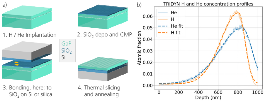
Crystal ion slicing (CIS) — implantation of helium and/or hydrogen ions to form a weakened buried layer, followed by thermal exfoliation — combined with plasma-activated direct wafer bonding (PADB) to an SiO2-coated target substrate. This mechanism decouples the crystalline GaP layer from its donor wafer, so the film can be integrated on arbitrary oxide-bearing substrates; a post-transfer anneal repairs implantation damage and restores the optical constants.
What would settle it
Fabricate a GaP-on-insulator rib or channel waveguide from an annealed film and measure its 1550 nm propagation loss; if the measured loss is several dB/cm or more — far above the 0.9 dB/cm material absorption — the material-quality or loss-estimation claim would need revisiting. Alternatively, measure the extinction coefficient directly via photothermal deflection or cavity ring-down on the same film.
Extended reading notes
Core claim
The central discovery is that combining crystal ion slicing (implanting He+ or H+/He+ to create a buried fracture plane) with plasma-activated direct wafer bonding transfers ~790 nm crystalline GaP films onto fused silica and SiO2/Si substrates, and that subsequent annealing at 600 °C restores the film's structural and optical properties. Reciprocal-space mapping and Raman spectroscopy show the implantation-induced strain and disorder largely relax after annealing; spectroscopic ellipsometry shows the refractive index shifts back toward bulk GaP and the extinction coefficient drops by one to two orders of magnitude, yielding an estimated plane-wave absorption loss of 0.9 dB/cm at 1550 nm. Th
Load-bearing premise
The 0.9 dB/cm loss and near-bulk n/k values rest on one Cody-Lorentz ellipsometric model fit to a single sample, and the extinction coefficient at 1550 nm is so small that modest errors in assumed thickness, roughness, or interface layer could shift the loss estimate.
Editorial extensions
If this is right
- GaP-on-insulator films can be made without epitaxial growth or sacrificial-layer release, removing substrate-architecture constraints on integration.
- Transferred films, after annealing, show near-bulk crystalline quality and low residual strain, suitable for nanophotonic fabrication.
- Optical dispersion approaches bulk GaP, with an estimated plane-wave absorption loss of 0.9 dB/cm at 1550 nm, compatible with low-loss telecom photonics.
- The wafer-bonding route is compatible with silicon photonics and back-end-of-line CMOS processing, easing heterogeneous integration.
- The platform is promising for visible-wavelength and nonlinear/quantum photonic devices that need GaP's high index, transparency, and second-order nonlinearity.
Reading between the lines
- The improved continuity of the H+/He+ co-implanted film hints that co-implantation helps layer separation, but the paper's two samples differ in both implantation and substrate; a controlled study on identical substrates would be needed to confirm that mechanism.
- The 0.9 dB/cm figure is a plane-wave material-absorption estimate, not a measured waveguide loss; real devices will also scatter from sidewall roughness, so waveguide measurements are the next test.
- If donor wafers can be re-polished and reused, this process could make crystalline GaP films economical for large-scale heterogeneous photonic integration.
- The same CIS+PADB sequence might transfer other III-V crystals or orientation-patterned GaP, potentially extending the approach to quasi-phase-matched nonlinear devices.
Editorial analysis
A structured set of objections, weighed in public.
Referee Report
Summary. The paper demonstrates fabrication of GaP-on-insulator thin films by crystal ion slicing (CIS) combined with plasma-activated direct wafer bonding, using both He+ and H+/He+ implanted donors bonded to fused silica and SiO2/Si substrates. The authors characterize the transferred films by SEM, AFM, IR/optical microscopy, XRD reciprocal space mapping, Raman spectroscopy, and spectroscopic ellipsometry. They report that post-transfer annealing at 600 °C substantially restores crystalline order, relieves implantation-induced strain, and brings the refractive index and extinction coefficient close to those of epitaxially grown GaP, with an estimated plane-wave absorption loss of 0.9 dB/cm at 1550 nm. The central claim is that this process provides a flexible, scalable route to low-loss GaP-on-insulator photonic substrates.
Significance. If the reported 0.9 dB/cm material absorption is reliable, the CIS+PADB process would represent a practically useful alternative to epitaxial growth and sacrificial-layer transfer for GaP photonic integration, with potential backend-of-line CMOS compatibility. The structural characterization is internally consistent: XRD RSM and Raman both show recovery after annealing, and the paper is unusually careful in acknowledging limitations, including the selection of the better of two films, the anomalously high extinction of the bulk reference, and the model-dependence of small k values. The transfer proof-of-concept on two substrate types is a useful contribution. However, the headline loss figure rests on a single ellipsometric fit without uncertainty analysis, which weakens the quantitative claim.
major comments (4)
- [Results, Fig. 4 discussion and Methods/Ellipsometry] The 0.9 dB/cm at 1550 nm is derived from the extinction coefficient k of one annealed film via a single Cody-Lorentz fit, with no reported confidence intervals or sensitivity analysis. At k ≈ 2.5×10⁻⁶, the extraction is highly sensitive to assumed thickness, roughness, interface layers, and dispersion model. The paper itself states for the bulk reference that 'small k values are particularly sensitive to measurement uncertainty and ellipsometric model assumptions' (Results, Fig. 4 discussion). That caveat applies equally to the thin-film k, but it is not propagated into the 0.9 dB/cm figure. Please provide a quantitative sensitivity analysis or reframe the claim as a model-dependent upper-limit estimate rather than a measured material loss.
- [Methods/Ellipsometry; Fig. 4] The Cody-Lorentz model was developed for amorphous semiconductors. Applying it to a crystalline GaP film may force an Urbach-tail shape in the transparent region, potentially biasing the small near-infrared k. This is load-bearing because the 0.9 dB/cm figure is presented as the key metric of photonic utility. Please justify the model choice for crystalline GaP, compare with alternative dispersion models (e.g., Lorentz oscillator or Tauc-Lorentz), or restrict the reported loss to a range where the model is validated against independent measurements (e.g., waveguide cutback or photothermal deflection).
- [Results, 'selected for subsequent analyses' and Abstract/Conclusions] The ellipsometric analysis was performed on a single H+/He+ co-implanted film on fused silica, which was selected as the better of the two transferred specimens. The paper explicitly states that this selection does not support a general comparison of implantation schemes, but the abstract and conclusions present the 0.9 dB/cm value as a property of the process without this single-sample qualifier. Please state in the abstract and conclusions that the loss value is measured on one representative film, or provide additional samples to support the process-level claim.
- [Fig. 3 and accompanying RSM discussion] The annealed thin film shows broader RSM peak widths (FWHM(Qx)/(2π)=1.14×10⁻² nm⁻¹, FWHM(Qz)/(2π)=1.30×10⁻² nm⁻¹) than both the pristine bulk and the unannealed film (Qx=2.84×10⁻³, Qz=8.42×10⁻³ nm⁻¹). The text attributes this to remaining strain gradients, but this broadening is in tension with the claim of 'near-bulk crystalline quality' based on XRD. The Raman LO linewidth recovery is convincing, but please clarify whether the RSM broadening after annealing represents a real degradation in long-range order or a fitting artifact, and how it is reconciled with the low optical loss.
minor comments (4)
- [Supplementary Information, Fig. S1 text] The SI text refers to 'bonding to a silica substrate (Fig. 3b)' and similar cross-references; these should be Fig. S1b/S1c, not Fig. 3b/3c. Please correct the figure numbering.
- [Abstract and Methods] The conversion from extinction coefficient k to dB/cm is not explicitly given. Please include the formula and state the assumed wavelength and refractive-index dispersion used in the conversion (e.g., α = 4πk/λ · 10/ln10 · 100 for dB/cm).
- [Methods/Material Preparation] The fluence is written as '1 × 10¹⁷ ions cm⁻²' in several places; use consistent superscript formatting. Also, 'BMFTR' in the Acknowledgements appears to be a typo for 'BMBF'.
- [Fig. 4] The red dotted line in the lower panel is described as 'wavelength dependent plane wave propagation loss' but the axis label is not visible in the text. Please ensure the secondary axis is labeled and that the loss curve is not confused with the extinction coefficient data.
Circularity Check
No circularity; all central claims are experimental characterizations, and the 0.9 dB/cm figure is a clearly labelled model-derived estimate.
full rationale
The paper makes no first-principles derivation whose output is equivalent to its input. Its central claims are empirical: CIS+PADB transfer is evidenced by IR/OM/SEM/AFM, RSM, Raman, and spectroscopic ellipsometry. RSM and Raman results are internally consistent and are compared with pristine bulk GaP and an external GaP-on-sapphire benchmark [17]. The 0.9 dB/cm loss at 1550 nm is explicitly described as being calculated from the extinction coefficient of the annealed film (Conclusions: 'The wavelength-dependent plane-wave propagation loss, calculated from the extinction coefficient of the annealed film, reaches 0.9 dB/cm'), i.e., it is a standard data-reduction formula, not a fitted parameter renamed as a prediction. The ellipsometric fit (Cody-Lorentz model, Methods) is an external modelling assumption, not a parameter defined by the loss value; the loss is not fed back into the fit. The paper itself flags the sensitivity of small k: 'small k values are particularly sensitive to measurement uncertainty and ellipsometric model assumptions, contributions from fitting artifacts, surface roughness, or backside reflections cannot be excluded' (Results, Fig. 4 discussion). That is a robustness/correctness limitation on the 0.9 dB/cm estimate, not circularity. The only self-citation is [25], used to support general PADB reliability in the Methods; it is not load-bearing for the transferred-film quality or the loss value. The acknowledged confound between implantation scheme and substrate (Results) is an experimental-design caveat, not a circular step. No self-definitional, predicted-from-fit, self-citation-chain, or renaming pattern is present.
Assumptions & free parameters
free parameters (1)
- Cody-Lorentz dispersion model parameters for the transferred GaP film (band gap, broadening, amplitudes, plus film thick =
Not enumerated
assumptions (3)
- domain assumption The Cody-Lorentz dispersion model is an adequate representation of the dielectric function of the ion-damaged and annealed GaP film over 400-2200 nm.
- domain assumption Ion implantation at 1e17 cm-2 (He at 105 keV, H at 70 keV) creates a buried cleavage plane while leaving the top ~790 nm layer transferable and recrystallizable.
- standard math Plane-wave absorption coefficient alpha = 4*pi*k/lambda, with complete optical confinement, gives an upper bound for waveguide material loss.
Cite this review
Pith. "Pith review of Direct Wafer Bonding of Crystal-Ion-Sliced GaP Thin Films for Photonic Applications." pith.science (2026). https://pith.science/paper/3XRWXZ4H
@misc{pith2026260802251,
  author       = {Pith},
  title        = {Pith review of: Direct Wafer Bonding of Crystal-Ion-Sliced GaP Thin Films for Photonic Applications},
  year         = {2026},
  howpublished = {\url{https://pith.science/paper/3XRWXZ4H}},
  note         = {Machine review of arXiv:2608.02251}
}
abstract
Gallium phosphide (GaP) is a promising material platform for integrated photonics because of its high refractive index, broad optical transparency, and strong second-order nonlinear response. Here, we demonstrate GaP-on-insulator thin films fabricated by crystal ion slicing and direct wafer bonding, using fused silica and SiO$_2$/Si/Si thermally oxidized silicon substrates as representative platforms. Unlike GaP thin-film platforms that rely on heteroepitaxial growth or sacrificial-layer release, the presented approach enables the flexible integration of crystalline GaP thin films, independent of both donor and target substrates. Following post-transfer annealing, the films exhibit near-bulk crystalline quality with low residual strain, smooth surfaces suitable for nanophotonic fabrication, and homogeneous bonding interfaces. Furthermore, annealing restores the linear optical dispersion (n and k) approaching that of epitaxially grown GaP with estimated plane wave absorption loss of 0.9 dB/cm at 1550 nm in the telecom C-band. The demonstrated approach establishes a scalable pathway toward high-quality GaP thin-film photonics compatible with versatile heterogeneous integration and back-end-of-line CMOS processing.
Figures


Figures from the paper (1 more)

Reference graph
Works this paper leans on
-
[1]
A review of gallium phosphide nanophotonics towards omnipotent nonlinear devices,
Y . Wang et al., "A review of gallium phosphide nanophotonics towards omnipotent nonlinear devices," Nanophotonics, vol. 13, no. 18, pp. 3207–3252, 2024
2024
-
[2]
Integrated gallium phosphide nonlinear photonics,
D. J. Wilson et al., "Integrated gallium phosphide nonlinear photonics," Nat. Photonics, vol. 14, no. 1, pp. 57–62, 2020
2020
-
[3]
Comparison of Harmonic Generation from Crystalline and Amorphous Gallium Phosphide Nanofilms,
B. Tilmann et al., "Comparison of Harmonic Generation from Crystalline and Amorphous Gallium Phosphide Nanofilms," Advanced Optical Materials, vol. 11, no. 16, p. 2300269, 2023
2023
-
[4]
Gallium Phosphide-on-Silicon Dioxide Photonic Devices,
K. Schneider, P. Welter, Y . Baumgartner, H. Hahn, L. Czornomaz, and P . Seidler, "Gallium Phosphide-on-Silicon Dioxide Photonic Devices," J. Lightwave Technol., vol. 36, no. 14, pp. 2994–3002, 2018
2018
-
[5]
Continuous-Wave Second-Harmonic Generation in Orientation- Patterned Gallium Phosphide Waveguides at Telecom Wavelengths,
Konstantinos Pantzas * et al., "Continuous-Wave Second-Harmonic Generation in Orientation- Patterned Gallium Phosphide Waveguides at Telecom Wavelengths," vol. 9, no. 6, pp. 2032– 2039, 2022
-
[6]
Bridging the Gap between Dielectric Nanophotonics and the Visible Regime with Effectively Lossless Gallium Phosphide Antennas,
J. Cambiasso, G. Grinblat, Y . Li, A. Rakovich, E. Cortés, and S. A. Maier, "Bridging the Gap between Dielectric Nanophotonics and the Visible Regime with Effectively Lossless Gallium Phosphide Antennas," Nano letters, vol. 17, no. 2, pp. 1219–1225, 2017
2017
-
[7]
Continuous Wave Second Harmonic Generation Enabled by Quasi-Bound- States in the Continuum on Gallium Phosphide Metasurfaces,
A. P. Anthur et al., "Continuous Wave Second Harmonic Generation Enabled by Quasi-Bound- States in the Continuum on Gallium Phosphide Metasurfaces," Nano letters, vol. 20, no. 12, pp. 8745–8751, 2020
2020
-
[8]
Integrated chirped photonic-crystal cavities in gallium phosphide for broadband soliton generation,
A. Nardi et al., "Integrated chirped photonic-crystal cavities in gallium phosphide for broadband soliton generation," Optica, vol. 11, no. 10, p. 1454, 2024
2024
Show all 27 references
-
[9]
Gallium phosphide photonic crystal nanocavities in the visible,
K. Rivoire, A. Faraon, and J. Vuckovic, "Gallium phosphide photonic crystal nanocavities in the visible," Applied Physics Letters, vol. 93, no. 6, p. 63103, 2008
2008
-
[10]
Gallium phosphide optical metasurfaces for visible light applications,
M. Melli et al., "Gallium phosphide optical metasurfaces for visible light applications," Scientific reports, vol. 10, no. 1, p. 20694, 2020
2020
-
[11]
Second harmonic generation in monolithic gallium phosphide metasurfaces,
M. Yang et al., "Second harmonic generation in monolithic gallium phosphide metasurfaces," Nanophotonics, vol. 13, no. 18, pp. 3311–3319, 2024
2024
-
[12]
Gallium phosphide-on-insulator integrated photonic structures fabricated using micro-transfer printing,
M. Billet et al., "Gallium phosphide-on-insulator integrated photonic structures fabricated using micro-transfer printing," Opt. Mater. Express, vol. 12, no. 9, p. 3731, 2022
2022
-
[13]
Octave-spanning supercontinuum generation from sub-millimeter-length integrated gallium phosphide waveguides,
X. Zhang et al., "Octave-spanning supercontinuum generation from sub-millimeter-length integrated gallium phosphide waveguides," Nature communications, vol. 16, no. 1, p. 10155, 2025. 11
2025
-
[14]
Microwave-to-optical conversion with a gallium phosphide photonic crystal cavity,
S. Hönl, Y . Popoff, D. Caimi, A. Beccari, T. J. Kippenberg, and P. Seidler, "Microwave-to-optical conversion with a gallium phosphide photonic crystal cavity," Nature communications, vol. 13, no. 1, p. 2065, 2022
-
[15]
Ultra-low-noise microwave to optics conversion in gallium phosphide,
R. Stockill et al., "Ultra-low-noise microwave to optics conversion in gallium phosphide," Nature communications, vol. 13, no. 1, p. 6583, 2022
2022
-
[16]
Review of Highly Mismatched III-V Heteroepitaxy Growth on (001) Silicon,
Y . Du et al., "Review of Highly Mismatched III-V Heteroepitaxy Growth on (001) Silicon," Nanomaterials, vol. 12, no. 5, 2022
2022
-
[17]
Directly grown crystalline gallium phosphide on sapphire for nonlinear all-dielectric nanophotonics,
D. Khmelevskaia et al., "Directly grown crystalline gallium phosphide on sapphire for nonlinear all-dielectric nanophotonics," Applied Physics Letters, vol. 118, no. 20, 2021
2021
-
[18]
Fabrication of Single Crystal Gallium Phosphide Thin Films on Glass,
H. Emmer et al., "Fabrication of Single Crystal Gallium Phosphide Thin Films on Glass," Scientific reports, vol. 7, no. 1, p. 4643, 2017
2017
-
[19]
Generation of even and odd high harmonics in resonant metasurfaces using single and multiple ultra-intense laser pulses,
M. R. Shcherbakov et al., "Generation of even and odd high harmonics in resonant metasurfaces using single and multiple ultra-intense laser pulses," Nature communications, vol. 12, no. 1, p. 4185, 2021
2021
-
[20]
Smart Cut™: Review on an attractive process for innovative substrate elaboration,
H. Moriceau, F. Mazen, C. Braley, F. Rieutord, A. Tauzin, and C. Deguet, "Smart Cut™: Review on an attractive process for innovative substrate elaboration," Nucl. Instrum. Methods Phys. Res., Sect. B, vol. 277, pp. 84–92, 2012
2012
-
[21]
Transfer of thin film gallium phosphide onto glass for integrable optical filters,
Maanav Ganjoo, John A. Carlson, Saoud A. Al-Mulla, James Brown, Brian T. Cunningham, John M. Dallesasse, "Transfer of thin film gallium phosphide onto glass for integrable optical filters," International Conference on Compound Semiconductor Manufacturing Technology, CS MANTECH...
2020
-
[22]
The Raman spectrum of gallium phosphide,
M.V . Hobden, J.P. Russell, "The Raman spectrum of gallium phosphide," Physics Letters, vol. 13, no. 1, pp. 39–41, 1964
1964
-
[23]
[Online]
"GaP," SurfaceNet GmbH, (n.d.). [Online]. Available: http://www.surfacenet.de/
-
[24]
Modeling of direct wafer bonding: Effect of wafer bow and etch patterns,
K. T. Turner and S. M. Spearing, "Modeling of direct wafer bonding: Effect of wafer bow and etch patterns," Journal of Applied Physics, vol. 92, no. 12, pp. 7658–7666, 2002
2002
-
[25]
Technical layout and fabrication of a compact all-glass four-channel beam splitter based on a Kösters design,
C. Rothhardt et al., "Technical layout and fabrication of a compact all-glass four-channel beam splitter based on a Kösters design," CEAS Space J, vol. 14, no. 2, pp. 287–301, 2022
2022
-
[26]
New optical dispersion models for the accurate description of the electrical permittivity in direct and indirect semiconductors,
K. Lizárraga et al., "New optical dispersion models for the accurate description of the electrical permittivity in direct and indirect semiconductors," J. Phys. D: Appl. Phys., vol. 56, no. 36, p. 365106, 2023
2023
-
[27]
Analytical model for the optical functions of amorphous semiconductors from the near infrared to ultraviolet Applications in thin film photovoltaics,
A. S. Ferlauto et al., "Analytical model for the optical functions of amorphous semiconductors from the near infrared to ultraviolet Applications in thin film photovoltaics," J. Appl. Phys., vol. 92, no. 5, pp. 2424–2436, 2002. 12 Supplementary Information: Direct Wafer Bondin...
2002
Reviewed August 4, 2026 · model on record in the stance chip above.
Discussion (0). Continue with ORCID to comment.