REVIEW 3 major objections 4 minor 66 references
One-dimensional Dirac modes in the core of a pentagonal topological crystalline insulator nanowire
T0 review · 3 major / 4 minor · reviewed 2026-08-07 · deepseek-v4-flash
Pith's one-line read Pentagonal SnTe-class nanowires with cationic twin planes are predicted to host two spatially separated one-dimensional helical Dirac crossings—one at the wire core and one at the outer surface—whenever the bulk band structure is inverted.
desk verdict A solid idealized-model prediction of two spatially separated helical Dirac channels in pentagonal TCI nanowires, with the main open question being how the ~2% closure strain affects the narrow alloy gap. read the letter →
The pith
A machine-rendered reading of the paper's core claim, the machinery that carries it, and where it could break.
The reading
What carries the argument
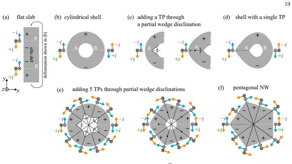
The load-bearing object is the odd set of five helical channels localized at the edges of the five cationic twin planes. Under the fivefold rotational symmetry $C_5$ of the ideal nanowire, the Hamiltonian block diagonalizes into sectors labeled by eigenvalues $\lambda_\nu = e^{-i\pi(2\nu+5)/5}$; the self-conjugate $\nu=0$ sector has eigenvalue $-1$ and, by time-reversal and mirror constraints, its mass term $\Delta_0$ must vanish, forcing a linear crossing. The paper proves that this $C_5=-1$ block is equivalent, up to the small strain used to close the pentagon, to a cylindrical SnTe shell containing a single twin plane with a twisted seam hopping, so the two crossings of the shell are the core and surface crossings of the nanowire. A complementary selection rule from the axial atomic column (spin plus orbital plus site phase must equal $5/2$ modulo 5) shows that $s$ and $p$ orbitals on the central column cannot contribute to the core mode, which is carried by surrounding atomic rings.
What would settle it
Tunneling or angle-resolved photoemission maps on a 50-nm-thick pentagonal Pb0.4Sn0.6Te nanowire whose twin-plane sublattice is identified by atomically resolved imaging: the predicted signature is two linearly dispersing crossings at the zone center, one localized near the wire axis and one at the surface hinges, present for cationic twin planes and absent for anionic twin planes. Finding a gap in the cationic wire, or crossings in the anionic wire, would rule out the mechanism as stated. A simpler numerical check is a calculation that includes the deformation-potential corrections the paper omits: if the inverted gap closes, the modes vanish.
Extended reading notes
Core claim
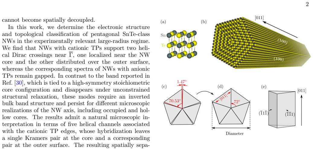
The central claim is that a pentagonal SnTe-class nanowire with cationic {111} twin planes and an inverted bulk band structure has two spatially separated helical Dirac crossings near the zone center $\Gamma$: one localized at the wire core and one at the outer surface, each consisting of a single time-reversal-protected Kramers pair. The crossings are not features of the specific core termination: they survive for occupied and hollow cores, and the core crossing has zero weight on the axial atomic column in the p-orbital model. The anionic-twin-plane wire shows no such crossings, and the same geometry in topologically trivial PbTe does not. The paper interprets the two modes as the inner and outer boundaries of an effective quantum-spin-Hall-like ribbon, with the five helical twin-plane-edge channels reorganizing under fivefold rotation into two gapped conjugate sectors and one self-conjugate sector that is forced to be gapless.
Load-bearing premise
The prediction assumes the roughly 2% uniaxial strain that closes the five wedges into a regular pentagon does not close or reorder the inverted bulk gap—strain-induced gap changes are estimated at 10-20% and dropped from the Hamiltonian—and that wires with cationic twin planes can actually be grown, although the paper's own DFT calculations find anionic twin planes energetically preferred in SnTe.
Editorial extensions
If this is right
- Cationic-twin-plane pentagonal SnTe-class nanowires provide an experimentally accessible realization of two spatially separated helical one-dimensional channels, one along the axial defect and one along the surface.
- The core helical mode persists across the microscopic core realizations studied (occupied and hollow), so its existence does not depend on the central atomic column or on dangling-bond states.
- In Pb0.4Sn0.6Te the two modes decouple exponentially with wire thickness, reaching well-developed massless dispersions at about 50 nm, within the experimentally grown thickness range.
- Nonmagnetic disorder and moderate structural distortions cannot gap a single helical Kramers pair by themselves, so the crossings are expected to persist as long as the protecting bulk and twin-plane gaps stay open.
- The Z-sector spectrum remains gapped for both twin-plane types, so the gapless physics is specific to the $\Gamma$ sector and the core/surface pair.
Reading between the lines
- The odd-channel counting suggests a general rule: any multiply twinned nanowire whose $n$-fold rotation axis meets an odd number of twin planes should leave one gapless helical pair in the self-conjugate rotational sector, whereas an even-numbered analogue would be fully gapped at the center by the same logic.
- If the core and surface modes can be selectively coupled to a superconductor and to magnets, the geometry is a natural testbed for Majorana bound states, since the two channels are spatially separated and could be gated or proximity-coupled independently—an extension the paper only sketches.
- The energetic preference for anionic twin planes found in the paper's DFT calculations is the main experimental hurdle; alloy composition or growth conditions might flip this preference, which would be a concrete target for growth studies.
- The exponential anticrossing fit suggests a simple design rule: the required wire thickness scales with the inverse localization length of the boundary states, so larger-gap alloys will need thicker wires.
Editorial analysis
A structured set of objections, weighed in public.
Referee Report
Summary. The paper studies pentagonal IV–VI nanowires built from five rocksalt wedges separated by radial {111} twin planes meeting at the wire axis. Tight-binding calculations with a minimal p3 model and a material-specific sp3d5 model show that, when the bulk band structure is inverted and the twin planes are cationic, the nanowire spectrum contains two helical Dirac crossings at the Gamma point: one localized near the core and one at the outer surface. For anionic twin planes the corresponding spectra remain gapped. The authors attribute the crossings to five helical twin-plane-edge channels whose C5 decomposition leaves a gapless self-conjugate sector, with the vanishing mass Delta_0 = 0 following from symmetry in Eq. (7). The mechanism is corroborated by C5-resolved spectra, a single-TP shell calculation that embeds as the C5 = -1 sector, and a PbTe control calculation. Material-specific calculations for Pb0.4Sn0.6Te predict well-developed modes at thicknesses of about 50 nm, and DFT calculations are used to compare structural stability of core and twin-plane configurations.
Significance. The central existence result is well supported: the two crossings are directly visible in the TB spectra of Fig. 3(a), they belong to the predicted C5 = -1 sector in Fig. 9, and the low-energy argument in Eqs. (4)-(7) is a clean symmetry derivation. The paper also includes strong controls: anionic twin planes, topologically trivial PbTe, occupied versus hollow cores, and DFT comparison with the earlier core-chain band of Ref. [30]. If the prediction survives quantitative strain and stability checks, it identifies a realistic nanowire geometry with spatially separated helical channels, which is an interesting analogue of a quantum spin Hall ribbon and potentially relevant for Majorana proposals. The main limitations are also acknowledged in the manuscript: the idealized strain treatment and the DFT result that anionic twin planes are energetically favored for SnTe. These caveats do not undermine the symmetry-based existence proof, but they do affect the strength of the experimental-accessibility claim.
major comments (3)
- [Section III and Section IV D] The central prediction for Pb0.4Sn0.6Te depends on the approximately 104 meV inverted bulk gap surviving the roughly 2% closure strain. However, the TB Hamiltonian includes only bond-orientation changes; deformation potentials, Poisson strain, and Slater-Koster bond-length rescaling of hoppings are estimated to change the gap by less than 10-20% and are then dropped. This estimate is not a calculation, and uniaxial strain can split the projected L valleys, so the statement in Section III that the corrections "do not alter the band ordering" is an assertion. Because Fig. 7(e) shows that removing bulk inversion removes both crossings, this is a load-bearing assumption. Please compute the p3 and sp3d5 gaps under the applied strain with deformation potentials and distance-rescaled hoppings, or provide a worst-case bound that demonstrates the band ordering remains inverted.
- [Abstract, Conclusions, and Appendix D] The abstract and conclusions describe these modes as establishing an "experimentally accessible realization" of spatially separated helical channels, but the DFT calculations in Fig. 18 find that for the investigated SnTe structures the anionic-TP configuration is energetically favored, and the entire predicted mode structure requires cationic twin planes. The paper acknowledges this as a challenge, but it does not provide evidence that cationic twin planes can be stabilized in Pb0.4Sn0.6Te or under realistic growth conditions. Please either give a quantitative argument for how the TP sublattice preference depends on alloy composition or growth conditions, or explicitly reframe the central claim as a conditional prediction for cationic-TP wires. As written, the experimental-accessibility claim goes beyond the evidence presented.
- [Eq. (8) and Fig. 7(c)] The statement that the modes are "well developed" at approximately 50 nm and above is based on an exponential fit to four thicknesses with a single decay constant and no reported uncertainty. Four points over a range whose largest value is the quoted 50 nm is a thin basis for the extrapolation "and above," especially because the sp3d5 alloy model itself inherits the approximate strain treatment discussed above. Please report the fit residuals, include additional thicknesses if possible, and state more cautiously that the 50 nm estimate is specific to the virtual-crystal sp3d5 model with the adopted strain approximations.
minor comments (4)
- [Fig. 3(b) and Section IV A] The anionic-TP spectrum in Fig. 3(b) is shown only after applying a 40 meV onsite shift to core orbitals, and the unshifted spectrum is not shown. Because this is the main control for the gapped anionic case in the simplified model, please include the unshifted spectrum in an appendix or state explicitly why the shift cannot remove a protected crossing.
- [Appendix B, Eq. (B24)] The approximation arccos(1/3) approximately equals 2 pi/5 is central to identifying the single-TP shell with the C5 = -1 sector. Please state explicitly that the residual 1.47 degree difference per wedge is the same closure strain already imposed in the pentagonal geometry, so that the correspondence is quantitative rather than approximate in a separate sense.
- [Fig. 12] The labels H and F appear in the spectra of Fig. 12 but are not defined in the caption; please define them in the caption or point to the subsection where they are introduced.
- [General] The paper would benefit from a short statement in Section III about the number of k-points, convergence criteria, and the exact procedure used to extract the anticrossing Delta_ac in Fig. 7(c), since the main quantitative claim depends on that extraction.
Circularity Check
No significant circularity: the Dirac-mode claim is derived from explicit TB spectra and a symmetry constraint, not from a fitted parameter or self-citation chain.
full rationale
The central claim—two spatially separated helical Dirac crossings for cationic-TP pentagonal nanowires—is demonstrated numerically inside the paper: TB spectra in Fig. 3, C5-resolved spectra in Fig. 9, the single-TP shell in Fig. 4, and the material-specific sp3d5 model in Fig. 7, with anionic-TP and PbTe controls in Figs. 7(d,e). The low-energy model's key step is not fitted: Eq. (7) imposes Delta_nu = -Delta_{-nu} by time-reversal and C5 symmetry, so the self-conjugate sector nu=0 has Delta_0=0 and therefore a linear crossing (Eq. (6)). The equivalence between the C5=-1 block of the full nanowire and the single-TP shell is derived in Appendix B (Eqs. (B20)-(B27)) rather than assumed. The exponential fit Eq. (8) quantifies the core-surface anticrossing versus thickness; the 50 nm result is a direct calculation, not a fitted quantity renamed as a prediction. The only self-citation of note is Ref. [33] (by two of the present authors), used for the p3 parameter set and for the earlier cationic/anionic TP classification; the paper re-derives the TP-sublattice distinction in its own single-TP and full-nanowire spectra, so the citation is corroborative and not load-bearing. The approximate treatment of closure strain (deformation potentials estimated at 10-20% and dropped) is a modeling assumption and a robustness risk, but it is not a circular step: the prediction would fail if the gap reordered, but the existence of the modes is computed from the stated Hamiltonian, not imported as the conclusion. Overall, no step reduces by construction to its input.
Assumptions & free parameters
free parameters (4)
- Anticrossing decay rate gamma =
0.1065 nm^{-1}
- Core-region onsite shift (anionic-TP NW) =
40 meV within 1 nm of the axis
- Surface perturbation magnitudes (Figs. 5 and 12) =
not specified (weak electrostatic potentials of different magnitudes)
- Tight-binding parameter sets (p3 and sp3d5) =
bulk values; virtual-crystal average for the alloy
assumptions (5)
- domain assumption SnTe and Pb0.4Sn0.6Te have inverted bulk band gaps (TCI regime) with the band ordering used in the tight-binding models.
- domain assumption Cationic and anionic (111) twin planes have the distinct topological characters assigned in Ref [33]: cationic twin planes bind protected side-surface crossings near the Gamma analogue, anionic ones do not.
- ad hoc to paper The roughly 2% wedge deformation used to close the pentagonal cross section, with no deformation-potential, Poisson, or bond-length corrections, preserves the inverted band ordering.
- domain assumption The five twin planes meet at a single uncompensated cationic (or anionic) atomic column, and the electronic structure is described by a single-particle tight-binding Hamiltonian.
- standard math Spinful rotation acts with U(2pi) = -I, and the C5 block decomposition of Appendix B is valid for the nanowire Hamiltonian.
Cite this review
Pith. "Pith review of One-dimensional Dirac modes in the core of a pentagonal topological crystalline insulator nanowire." pith.science (2026). https://pith.science/paper/SMWCVY6T
@misc{pith2026260805908,
  author       = {Pith},
  title        = {Pith review of: One-dimensional Dirac modes in the core of a pentagonal topological crystalline insulator nanowire},
  year         = {2026},
  howpublished = {\url{https://pith.science/paper/SMWCVY6T}},
  note         = {Machine review of arXiv:2608.05908}
}
abstract
We investigate the electronic band topology of recently fabricated pentagonal IV-VI semiconductor nanowires, which contain five radial $\{111\}$ twin planes meeting at the nanowire axis. Tight-binding calculations show that, when the bulk band structure is inverted and the twin planes in the nanowire are cationic, the spectrum contains two spatially separated helical Dirac crossings near $\overline{\Gamma}$: one localized at the core and the other at the outer surface. When the twin planes are anionic, the corresponding spectra remain gapped. The crossings originate from the hybridization of five helical channels associated with the twin-plane edges, whose odd number leaves one Kramers pair near the nanowire axis and the other at the outer boundary. Realistic multiorbital calculations for $\mathrm{Pb}_{0.4}\mathrm{Sn}_{0.6}\mathrm{Te}$ predict well-developed core and surface modes at nanowire thicknesses of approximately 50~nm and above. These results establish pentagonal SnTe-class nanowires as an experimentally accessible realization of spatially separated helical channels bound to the axial defect and the outer boundary.
Figures


Figures from the paper (15 more)




Reference graph
Works this paper leans on
-
[30]
W. A. Benalcazar, B. A. Bernevig, and T. L. Hughes, Electric multipole moments, topological multipole mo- ment pumping, and chiral hinge states in crys- talline insulators, Phys. Rev. B96, 245115 (2017), arXiv:1708.04230
arXiv 2017
-
[1]
We label these lattice sites byn= 0,
Off-axis orbital content of theC 5 =−1sector Every off-axis atomic site belongs to an orbit of five sites related by successiveC 5 rotations. We label these lattice sites byn= 0, . . . ,4 in counterclockwise order when the cross section is viewed from the positive end of the NW axis toward the origin, so that an active coun- terclockwise rotation mapsnont...
-
[2]
,4 and ordered counterclockwise as shown in Fig
Block diagonalization of the pentagonal NW Hamiltonian We divide the pentagonal NW into five symmetry- related wedges, labeled by the indexn= 0, . . . ,4 and ordered counterclockwise as shown in Fig. 8. For clarity, we first present the block diagonalization for the case in which each wedge couples only to its two nearest neigh- boring wedges. The inclusi...
-
[3]
(B19) becomes H {0} NW =H 0 −T 01U5 −U † 5 T † 01.(B20) λ0 = −1 other λν C5 sectors NW with cat
Relation of theC 5 =−1sector to a single-TP shell Forν= 0, one hasλ 0 =−1, and Eq. (B19) becomes H {0} NW =H 0 −T 01U5 −U † 5 T † 01.(B20) λ0 = −1 other λν C5 sectors NW with cat. TPs NW with an. TPs (b) (a) FIG. 9. Rotationally resolved band structures of pentagonal SnTe NWs with (a) cationic and (b) anionic TPs. The spectra correspond to those shown in ...
-
[4]
Projected symmetries of the five-channel model We finally derive the symmetry matrices used in the k·ptheory near Γ. The basis consists of five helical Kramers pairs ordered counterclockwise around the NW, with a two-component spinor attached to each channel. The labeling is chosen so thatC 5 maps channelnonto n+ 1 and channeln= 0 lies in the mirror plane...
-
[5]
Closed-surface quantization We begin with a defect-free analogue of the single-TP shell, obtained by wrapping a SnTe (100) slab around the
-
[6]
Y. Ando and L. Fu, Topological crystalline insulators and topological superconductors: From concepts to materi- als, Annu. Rev. Condens. Matter Phys.6, 361 (2015), arXiv:1501.00531
arXiv 2015
-
[7]
Mirror-related TP-edge and face-midline channels The same gapped spectrum admits a complementary real-space interpretation. The cylindrical shell contain- ing one TP has two mirror planes relevant near Z: the mirror plane coinciding with the TP and a regular (01 ¯1) mirror plane on the opposite side of the shell. Consider a time-reversal-preserving surfac...
Show all 66 references
-
[8]
Doubled low-energy theory The hybridization of the ten channels near Z is de- scribed by a doubled version of the five-pair model intro- duced for the Γ sector in Eqs. (4)–(7). The two copies 17 (a) (b) +i +i −i −i − + − + − + − + −+ +i +i −i −i − +gap sign shell with a TP nea...
-
[9]
Geometric interpretation of the opposite velocities The relative signs of the TP-edge and face-midline ve- locities can be visualized through the geometric construc- tion shown in Fig. 14. All panels show cross sections in the (011) plane, while the domain-wall modes propagate...
-
[10]
The calculations are performed for the same pentagonal NW systems considered in the main text in Fig
Realistic-model confirmation Finally, we examine the spectra near Z in the material- specificsp 3d5 model. The calculations are performed for the same pentagonal NW systems considered in the main text in Fig. 7. Figure 15 shows the corresponding spectra for 50-nm-thick Pb 0.4S...
-
[11]
As shown schemat- ically in Fig
axis to form a cylindrical shell. As shown schemat- ically in Fig. 10(a), the local hopping amplitudes and onsite terms are kept identical to those of the correspond- ing unwrapped geometry, while the two ends of the trans- verse direction are connected by a rotated boundary h...
-
[12]
Wei and A
S.-H. Wei and A. Zunger, Electronic and structural anomalies in lead chalcogenides, Phys. Rev. B55, 13605 (1997)
1997
-
[13]
Sukhovatkin, S
V. Sukhovatkin, S. Hinds, L. Brzozowski, and E. H. Sar- gent, Colloidal quantum-dot photodetectors exploiting multiexciton generation, Science324, 1542 (2009)
2009
-
[14]
E. H. Sargent, Infrared photovoltaics made by solution processing, Nat. Photon.3, 325 (2009)
2009
-
[15]
O. E. Semonin, J. M. Luther, S. Choi, H.-Y. Chen, J. Gao, A. J. Nozik, and M. C. Beard, Peak external pho- tocurrent quantum efficiency exceeding 100% via MEG in a quantum dot solar cell, Science334, 1530 (2011)
2011
-
[16]
T. H. Hsieh, H. Lin, J. Liu, W. Duan, A. Bansil, and L. Fu, Topological crystalline insulators in the SnTe material class, Nat. Commun.3, 982 (2012), arXiv:1202.1003
2012 arXiv
-
[17]
Tanaka, Z
Y. Tanaka, Z. Ren, T. Sato, K. Nakayama, S. Souma, T. Takahashi, K. Segawa, and Y. Ando, Experimental realization of a topological crystalline insulator in SnTe, Nat. Phys.8, 800 (2012), arXiv:1206.5399
2012 arXiv
-
[18]
S.-Y. Xu, C. Liu, N. Alidoust, M. Neupane, D. Qian, I. Belopolski, J. D. Denlinger, Y. J. Wang, H. Lin, L. A. Wray, G. Landolt, B. Slomski, J. H. Dil, A. Marcinkova, E. Morosan, Q. Gibson, R. Sankar, F. C. Chou, R. J. Cava, A. Bansil, and M. Z. Hasan, Observation of a topo- lo...
2012 arXiv
-
[19]
Dziawa, B
P. Dziawa, B. J. Kowalski, K. Dybko, R. Buczko, A. Szczerbakow, M. Szot, E. Lusakowska, T. Balasub- ramanian, B. M. Wojek, M. H. Berntsen, O. Tjern- berg, and T. Story, Topological crystalline insulator states in Pb 1−xSnxSe , Nat. Mater.11, 1023 (2012), arXiv:1206.1705
2012 arXiv
-
[20]
Safaei, P
S. Safaei, P. Kacman, and R. Buczko, Topological crys- talline insulator (Pb,Sn)Te: Surface states and their spin polarization, Phys. Rev. B88, 045305 (2013), arXiv:1303.7119
2013 arXiv
-
[21]
J. Liu, T. H. Hsieh, P. Wei, W. Duan, J. Moodera, and L. Fu, Spin-filtered edge states with an electrically tun- able gap in a two-dimensional topological crystalline in- sulator, Nat. Mater.13, 178 (2014), arXiv:1310.1044
2014 arXiv
-
[22]
Ozawa, A
H. Ozawa, A. Yamakage, M. Sato, and Y. Tanaka, Topo- logical phase transition in a topological crystalline insula- tor induced by finite-size effects, Phys. Rev. B90, 045309 (2014), arXiv:1403.3791
2014 arXiv
-
[23]
Safaei, M
S. Safaei, M. Galicka, P. Kacman, and R. Buczko, Quantum spin Hall effect in IV-VI topological crys- talline insulators, New J. Phys.17, 063041 (2015), arXiv:1501.04728
2015 arXiv
-
[24]
Liu and L
J. Liu and L. Fu, Electrically tunable quantum spin Hall state in topological crystalline insulator thin films, Phys. Rev. B91, 081407(R) (2015), arXiv:1501.05632
2015 arXiv
-
[25]
Sessi, D
P. Sessi, D. Di Sante, A. Szczerbakow, F. Glott, S. Wil- fert, H. Schmidt, T. Bathon, P. Dziawa, M. Greiter, T. Neupert, G. Sangiovanni, T. Story, R. Thomale, and M. Bode, Robust spin-polarized midgap states at step edges of topological crystalline insulators, Science354, 1269...
2016 arXiv
-
[26]
Rechci´ nski and R
R. Rechci´ nski and R. Buczko, Topological states on un- even (Pb,Sn)Se (001) surfaces, Phys. Rev. B98, 245302 (2018), arXiv:1808.07779
2018 arXiv
-
[27]
Iaia, C.-Y
D. Iaia, C.-Y. Wang, Y. Maximenko, D. Walkup, R. Sankar, F. Chou, Y.-M. Lu, and V. Madhavan, Topo- logical nature of step-edge states on the surface of the topological crystalline insulator Pb0.7Sn0.3Se, Phys. Rev. 24 B99, 155116 (2019), arXiv:1809.10689
2019 arXiv
-
[28]
Brzezicki, M
W. Brzezicki, M. M. Wysoki´ nski, and T. Hyart, Topo- logical properties of multilayers and surface steps in the SnTe material class, Phys. Rev. B100, 121107(R) (2019), arXiv:1812.02168
2019 arXiv
-
[29]
W. A. Benalcazar, B. A. Bernevig, and T. L. Hughes, Quantized electric multipole insulators, Science357, 61 (2017), arXiv:1611.07987
2017 arXiv
-
[31]
Langbehn, Y
J. Langbehn, Y. Peng, L. Trifunovic, F. von Oppen, and P. W. Brouwer, Reflection-symmetric second-order topo- logical insulators and superconductors, Phys. Rev. Lett. 119, 246401 (2017), arXiv:1708.03640
2017 arXiv
-
[32]
Schindler, A
F. Schindler, A. M. Cook, M. G. Vergniory, Z. Wang, S. S. P. Parkin, B. A. Bernevig, and T. Neupert, Higher- order topological insulators, Sci. Adv.4, eaat0346 (2018), arXiv:1708.03636
2018 arXiv
-
[33]
Sadowski, P
J. Sadowski, P. Dziawa, A. Kaleta, B. Kurowska, A. Reszka, T. Story, and S. Kret, Defect-free SnTe topo- logical crystalline insulator nanowires grown by molec- ular beam epitaxy on graphene, Nanoscale10, 20772 (2018), arXiv:1812.08888
2018 arXiv
-
[34]
P. Liu, H. J. Han, J. Wei, D. Hynek, J. L. Hart, M. G. Han, C. J. Trimble, J. Williams, Y. Zhu, and J. J. Cha, Synthesis of narrow SnTe nanowires using alloy nanoparticles, ACS Appl. Electron. Mater.3, 184 (2021), arXiv:2010.08078
2021 arXiv
-
[35]
N. M. Nguyen, W. Brzezicki, and T. Hyart, Corner states, hinge states, and Majorana modes in SnTe nanowires, Phys. Rev. B105, 075310 (2022), arXiv:2105.11489
2022 arXiv
-
[36]
Hussain, K
G. Hussain, K. Warda, G. Cuono, and C. Autieri, Den- sity functional theory study of the spin–orbit insulating phase in SnTe cubic nanowires: Implications for topolog- ical electronics, ACS Appl. Nano Mater.7, 8044 (2024), arXiv:2308.15358
2024
-
[37]
Kawala and W
A. Kawala and W. Brzezicki, Topological properties of the [110] SnTe nanowires, Phys. Rev. B112, 035102 (2025), arXiv:2407.16421
2025 arXiv
-
[38]
S. G. Schellingerhout, R. Bergamaschini, M. A. Verhei- jen, F. Montalenti, L. Miglio, and E. P. A. M. Bakkers, In-plane nanowire growth of topological crystalline in- sulator Pb 1−xSnxTe, Adv. Funct. Mater.33, 2305542 (2023)
2023
-
[39]
M. G. C. Mientjes, L. M. van Dijk, F. J. Witmans, M. W. J. Hendriks, V. van de Sande, X. Guan, M. J. G. Kamphuis, J. Ridderbos, F. Nichele, M. A. Verheijen, A. Brinkman, F. A. Zwanenburg, and E. P. A. M. Bakkers, Structural and electrical properties of SnTe nanoflakes and nano...
2025
-
[40]
Hussain, G
G. Hussain, G. Cuono, P. Dziawa, D. Janaszko, J. Sad- owski, S. Kret, B. Kurowska, J. Polaczy´ nski, K. Warda, S. Sattar, C. M. Canali, A. Lau, W. Brzezicki, T. Story, and C. Autieri, Pentagonal nanowires from topological crystalline insulators: a platform for intrinsic core–s...
2024
-
[41]
Hofmeister, Fivefold twinned nanoparticles, in Encyclopedia of Nanoscience and Nanotechnology, Vol
H. Hofmeister, Fivefold twinned nanoparticles, in Encyclopedia of Nanoscience and Nanotechnology, Vol. 3, edited by H. S. Nalwa (American Scientific Publishers, Stevenson Ranch, CA, 2004) pp. 431–452
2004
-
[42]
Baletto and R
F. Baletto and R. Ferrando, Structural properties of nan- oclusters: Energetic, thermodynamic, and kinetic effects, Rev. Mod. Phys.77, 371 (2005)
2005
-
[43]
Samadi, R
S. Samadi, R. Rechci´ nski, and R. Buczko, Topological electronic structure of twin boundaries and twinning su- perlattices in the SnTe material class, Phys. Rev. B107, 205401 (2023), arXiv:2212.14640
2023 arXiv
-
[44]
de Wit, Partial disclinations, J
R. de Wit, Partial disclinations, J. Phys. C: Solid State Phys.5, 529 (1972)
1972
-
[45]
A. J. Miller, G. A. Saunders, and Y. K. Yogurtcu, Pres- sure dependences of the elastic constants of PbTe, SnTe and Ge 0.08Sn0.92Te , J. Phys. C: Solid State Phys.14, 1569 (1981)
1981
-
[46]
I. I. Zasavitskii, E. A. de Andrada e Silva, E. Abramof, and P. J. McCann, Optical deformation potentials for PbSe and PbTe, Phys. Rev. B70, 115302 (2004)
2004
-
[47]
Rabii, Energy-band structure and electronic properties of SnTe, Phys
S. Rabii, Energy-band structure and electronic properties of SnTe, Phys. Rev.182, 821 (1969)
1969
-
[48]
C. S. Lent, M. A. Bowen, J. D. Dow, R. S. Allgaier, O. F. Sankey, and E. S. Ho, Relativistic empirical tight-binding theory of the energy bands of GeTe, SnTe, PbTe, PbSe, PbS, and their alloys, Superlattices Microstruct.2, 491 (1986)
1986
-
[49]
Geier, I
M. Geier, I. C. Fulga, and A. Lau, Bulk-boundary-defect correspondence at disclinations in rotation-symmetric topological insulators and superconductors, SciPost Phys.10, 092 (2021), arXiv:2007.13781
2021 arXiv
-
[50]
Y. Ran, Y. Zhang, and A. Vishwanath, One-dimensional topologically protected modes in topological insulators with lattice dislocations, Nat. Phys.5, 298 (2009), arXiv:0810.5121
2009 arXiv
-
[51]
Slager, A
R.-J. Slager, A. Mesaros, V. Juriˇ ci´ c, and J. Zaanen, Inter- play between electronic topology and crystal symmetry: Dislocation-line modes in topological band insulators, Phys. Rev. B90, 241403(R) (2014), arXiv:1401.4044
2014 arXiv
-
[52]
Queiroz, I
R. Queiroz, I. C. Fulga, N. Avraham, H. Beidenkopf, and J. Cano, Partial lattice defects in higher-order topo- logical insulators, Phys. Rev. Lett.123, 266802 (2019), arXiv:1809.03518
2019 arXiv
-
[53]
T. I. Tuegel, V. Chua, and T. L. Hughes, Embedded topological insulators, Phys. Rev. B100, 115126 (2019), arXiv:1802.06790
2019 arXiv
-
[54]
Naselli, V
G. Naselli, V. K¨ onye, S. K. Das, G. G. N. Angilella, A. Isaeva, J. van den Brink, and C. Fulga, Nontrivial gapless electronic states at the stacking faults of weak topological insulators, Phys. Rev. B106, 094105 (2022), arXiv:2206.06765
2022 arXiv
-
[55]
A. K. Nayak, J. Reiner, R. Queiroz, H. Fu, C. Shekhar, B. Yan, C. Felser, N. Avraham, and H. Beidenkopf, Resolving the topological classification of bismuth with topological defects, Sci. Adv.5, eaax6996 (2019), arXiv:1903.00880
2019 arXiv
-
[56]
Zhang and A
Y. Zhang and A. Vishwanath, Anomalous Aharonov- Bohm conductance oscillations from topological insula- tor surface states, Phys. Rev. Lett.105, 206601 (2010), arXiv:1005.3542
2010 arXiv
-
[57]
S. S. Hong, Y. Zhang, J. J. Cha, X.-L. Qi, and Y. Cui, One-dimensional helical transport in topological insula- tor nanowire interferometers, Nano Lett.14, 2815 (2014), arXiv:1303.1601
2014 arXiv
-
[58]
S. Cho, B. Dellabetta, R. Zhong, J. Schneeloch, T. Liu, G. Gu, M. J. Gilbert, and N. Mason, Aharonov–Bohm os- cillations in a quasi-ballistic three-dimensional topolog- 25 ical insulator nanowire, Nat. Commun.6, 7634 (2015), arXiv:1409.5095
2015 arXiv
-
[59]
L. A. Jauregui, M. T. Pettes, L. P. Rokhinson, L. Shi, and Y. P. Chen, Magnetic field-induced helical mode and topological transitions in a topological insula- tor nanoribbon, Nat. Nanotechnol.11, 345 (2016), arXiv:1503.00685
2016 arXiv
-
[60]
Fu and C
L. Fu and C. L. Kane, Superconducting proximity ef- fect and Majorana fermions at the surface of a topo- logical insulator, Phys. Rev. Lett.100, 096407 (2008), arXiv:0707.1692
2008 arXiv
-
[61]
Fu and C
L. Fu and C. L. Kane, Josephson current and noise at a superconductor/quantum-spin-Hall- insulator/superconductor junction, Phys. Rev. B 79, 161408(R) (2009), arXiv:0804.4469
2009 arXiv
-
[62]
Xu and L
C. Xu and L. Fu, Fractionalization in Josephson junction arrays hinged by quantum spin Hall edges, Phys. Rev. B 81, 134435 (2010), arXiv:0911.1782
2010 arXiv
-
[63]
P. B. Littlewood, B. Mihaila, R. K. Schulze, D. J. Safarik, J. E. Gubernatis, A. Bostwick, E. Rotenberg, C. P. Opeil, T. Durakiewicz, J. L. Smith, and J. C. Lashley, Band structure of SnTe studied by photoemission spectroscopy, Phys. Rev. Lett.105, 086404 (2010), arXiv:1008.4148
2010 arXiv
-
[64]
J. Liu, W. Duan, and L. Fu, Two types of surface states in topological crystalline insulators, Phys. Rev. B88, 241303(R) (2013), arXiv:1304.0430
2013 arXiv
-
[65]
Kresse and J
G. Kresse and J. Hafner, Ab initio molecular dynamics for liquid metals, Phys. Rev. B47, 558(R) (1993)
1993
-
[66]
Kresse and J
G. Kresse and J. Furthm¨ uller, Efficient iterative schemes for ab initio total-energy calculations using a plane-wave basis set, Phys. Rev. B54, 11169 (1996)
1996
Reviewed August 7, 2026 · model on record in the stance chip above.
Discussion (0). Continue with ORCID to comment.