REVIEW 1 major objections 5 minor 54 references
Ion trap on borosilicate substrate with integrated femtosecond-laser-written waveguide
T0 review · 1 major / 5 minor · reviewed 2026-08-15 · deepseek-v4-flash
Pith's one-line read An ion trap built on borosilicate glass with an integrated femtosecond-laser-written waveguide traps 40Ca+ and drives coherent Rabi oscillations with 729 nm light delivered entirely through the on-chip optics.
desk verdict A credible, manufacturable ion-trap platform with in-plane FLW light delivery; the coherence claim needs one more datapoint, but the engineering is solid. read the letter →
The pith
A machine-rendered reading of the paper's core claim, the machinery that carries it, and where it could break.
The reading
What carries the argument
The load-bearing element is the femtosecond-laser-written (FLW) waveguide embedded in a separate borosilicate optics block that is bonded directly onto the trap surface, with the waveguide core inscribed at the $170$ $\mu$m ion height and running parallel to the electrode plane. This geometry lets light exit through the cleaved facet at the ion's position, eliminating the grating couplers or etched mirrors needed in planar waveguide approaches. Within the glass, guiding occurs in regions displaced above and below the laser-modified track, and the paper uses spherical aberration of the writing beam as a process parameter to control mode-field diameter down to roughly 3 $\mu$m. For the ion experiments, an actively aligned optical fiber is glued to the rear facet, and the coherent-drive evidence is a carrier Rabi curve analyzed with the thermal-state model $P_{|1\rangle}(t)=\sum_n P_n(\bar n)\sin^2(\Omega_{n,n}t/2)$, which assumes a single Rabi frequency and a thermal phonon distribution.
What would settle it
A Ramsey sequence using the integrated waveguide, compared with free-space delivery at the same Rabi frequency, would settle the coherence claim: if the waveguide-delivered coherence time is markedly shorter than the free-space value, the thermal-Rabi fit would have masked dephasing or beam instability. An even simpler check is to record the Rabi flop well beyond 300 $\mu$s and inspect whether the contrast follows the smooth thermal envelope of Eq. (2) or displays irregular distortions.
Extended reading notes
Core claim
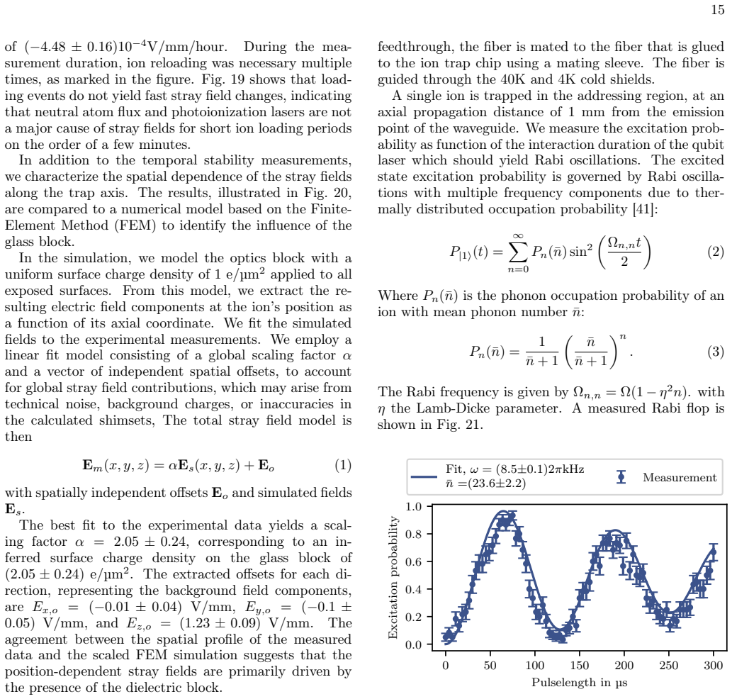
The central discovery is end-to-end functionality: the paper reports trapping of a $^{40}\mathrm{Ca}^+$ ion above a borosilicate surface trap, shuttling the ion to a zone roughly 1 mm in front of a bonded glass block that contains a femtosecond-laser-written waveguide, and driving the $S_{1/2} \leftrightarrow D_{5/2}$ qubit transition with 729 nm light delivered through that waveguide. The measured carrier Rabi oscillation, fitted with a thermal phonon distribution, yields a Rabi frequency of $\Omega = (8.5 \pm 0.1) \times 2\pi$ kHz at a mean phonon number of $\bar n = 23.6 \pm 2.2$. Supporting characterizations show that the waveguide can be single-mode at both 729 nm and 405 nm, that strongly confined modes tolerate bend radii down to about 6 mm with loss below 1 dB/cm, and that the bonded dielectric block shifts the RF null by less than a micrometer at a 1 mm standoff while producing stray electric fields with a slow, repeatable drift of about $-4.5 \times 10^{-4}$ V/(mm$\cdot$h). The authors frame the result as validating a route to integrated light delivery that is compatible with silicon wafers and with hybrid micro-optics for eventual single-ion addressing.
Load-bearing premise
The load-bearing premise is that the single measured Rabi curve can be trusted as evidence of coherent driving: the fit assumes a stable, single Rabi frequency and a thermal phonon distribution with no additional dephasing or intensity noise from the integrated delivery path, so a Ramsey or gate measurement is needed to confirm that the oscillation envelope is not mimicked by partially incoherent excitation.
Editorial extensions
If this is right
- The waveguide emits light at ion height along the trap axis, so the platform can route qubit light without out-of-plane couplers, removing a major fabrication constraint of planar integrated ion traps.
- Because the same writing process yields single-mode guidance at 405 nm, the optical layer should also be able to deliver Doppler-cooling, repumping, and state-preparation light, not just the 729 nm qubit beam.
- The low bending loss at a 6 mm radius of curvature allows compact routing of the waveguide within the glass block, which matters for scaling to many addressing zones on a single chip.
- The slowly drifting stray field from the dielectric block ($\sim -4.5\times10^{-4}$ V/(mm$\cdot$h)) means micromotion compensation stays valid for hours rather than minutes, an essential practical condition for using the platform in experiments.
- The measured beam radius of roughly 95 $\mu$m at the ion position makes the current device a global beam; the paper's stated compatibility with pick-and-place ball lenses is the proposed route to tight, per-ion addressing spots.
Reading between the lines
- Extension: If the waveguide path is truly phase-preserving, a Ramsey or spin-echo measurement through the same 729 nm waveguide at matched Rabi frequency should show the same or nearly the same coherence time as free-space delivery; this is a direct test the paper does not report.
- Extension: The unexplained secondary intensity peak near $x = 110$ $\mu$m in the ion-based profile, absent from the camera profile, suggests interference from the manually cleaved facet; a wave-optics simulation of the facet topography could predict and guide improvements to the cleaving step.
- Extension: Combining the demonstrated stray-field model with the measured charge-density drift could lead to a monitoring protocol that compensates the dielectric block's slow charging in real time using the axial stray-field position-modulation technique described in Appendix D.
- Extension: If laser-written waveguides can be inscribed in three dimensions through the bonded stack, the same architecture might deliver light from the chip edge directly into multiple trap zones, or even through vias, which would further reduce the free-space optics footprint in large arrays.
Signed reviews
Editorial analysis
A structured set of objections, weighed in public.
Referee Report
Summary. The paper reports a borosilicate-glass surface ion trap with an integrated femtosecond-laser-written (FLW) waveguide that delivers 729 nm qubit light to a 40Ca+ ion in a cryogenic setup. It describes the FLW waveguide fabrication and characterization, including mode-field-diameter tuning, bending-loss measurements, and single-mode guiding at 405 nm, as well as the design, simulation, and assembly of the trap with a bonded optics block. Cryogenic tests demonstrate trapping, shuttling to an addressing zone in front of the waveguide, low heating rates, characterization of stray fields caused by the dielectric block, and Rabi oscillations driven by the integrated light path. The authors position this as an end-to-end demonstration of a scalable route to integrated light delivery for trapped-ion devices.
Significance. If fully supported, this work is a valuable engineering contribution: physically separating the optical delivery layer from the electrode substrate and bonding it on top is a practical approach that remains compatible with silicon/ASIC integration, and the FLW waveguide characterization (tunable MFD, low bending loss at small radii, single-mode operation at 405 nm) provides useful process data for the community. The cryogenic measurements of heating rates and stray fields, together with the axial secular-frequency validation in Appendix C, add solid quantitative grounding. The core novelty is the demonstration that an ion can be trapped, shuttled, and driven by light from an integrated FLW waveguide in a cryogenic environment; this goes beyond previous planar waveguide demonstrations and is of clear interest to integrated trapped-ion quantum computing. However, the headline claim of coherent qubit dynamics rests on limited evidence, as detailed below.
major comments (1)
- [Sec. IV C, Fig. 21] The central claim of coherent qubit dynamics driven by the integrated waveguide rests entirely on a single Rabi-flop curve fitted with the thermal carrier model of Eqs. (2)-(3). No repetition statistics, no independent measurement of the mean phonon number nbar at the same position and time, and no comparison with an incoherent or dephased excitation model are provided. A decaying oscillatory curve with a high fitted nbar can in principle be reproduced by partially incoherent excitation if the effective linewidth happens to match, so the data as presented do not uniquely establish phase coherence. Since the abstract and conclusions state 'coherent qubit operations' as a headline result, please either add supporting evidence (e.g., a Ramsey or spin-echo measurement, or at least several repeated Rabi curves with an explicit model comparison against an incoherent saturating-exponential model), or moderate the claim in the abstract and conclusions to 'resonant excitation' via the integrated waveguide.
minor comments (5)
- [Sec. II C, Figs. 4-6] Several waveguide characterization figures (e.g., Fig. 4 and Fig. 6) present data without error bars or a statement about repeatability; Fig. 5 mentions mean and standard error, but the same clarity should be provided for all parameter sweeps so that the claimed mode-size tuning range and bending-loss thresholds can be critically assessed.
- [Sec. IV C, Fig. 22] The camera beam profile is rescaled to match the ion-based Rabi-frequency data before being compared, and the secondary intensity peak near x = 110 um in the ion data is absent in the camera profile; the phrase 'good agreement' should be softened to acknowledge this discrepancy and the fact that the comparison tests only shape, not absolute intensity.
- [Sec. IV B, Fig. 20 and Eq. (1)] The stray-field model uses a global scaling factor alpha and per-axis offsets E_o fitted to the same data from which the surface charge density (2.05 +/- 0.24) e/um^2 is inferred. Although this is a fit rather than a circular derivation, the authors should report the fit quality (residuals or reduced chi-square) and discuss how identifiable alpha is given that the fitted z-offset of 1.23 V/mm is not negligible.
- [General] There are numerous typographical and notation issues, including '42S1/2↔3 2D5/2' in Sec. IV C (missing superscripts), 'wavelenght' in the Fig. 21 caption, 'Beding loss' in Fig. 6, and 'The its show' in Appendix D; please correct these throughout.
- [Sec. IV C, Fig. 21 caption] The caption of Fig. 21 lists the fit parameters as 'ω = (8.5±0.1)2πkHz, n̄ =(23.6±2.2)' but the symbol ω is elsewhere used for secular frequencies; the Rabi frequency should be denoted Ω for consistency and the units should be written explicitly as 2π × kHz.
Circularity Check
No significant circularity: the paper's central claims are direct measurements with explicit fits, and no prediction reduces by construction to its inputs.
full rationale
The paper's load-bearing results are direct experimental measurements: waveguide transmission and mode-field diameters are measured with cameras and beam profilers; heating rates are measured by sideband thermometry; stray fields are measured by micromotion compensation; and the integrated qubit drive is demonstrated by a measured carrier Rabi flop (Fig. 21) fit to the standard thermal carrier model of Eqs. (2)-(3). That fit returns Omega and nbar from the same curve, but the paper presents it as a fit, not as a prediction of an independent quantity, and no fitted parameter is renamed as a validated prediction. The stray-field analysis in Eq. (1) explicitly fits a global scale factor alpha and spatial offsets to the measured field data; the inferred 2 e/um^2 surface charge density is a fitted parameter of a model, not a self-defined target. The camera-profile comparison in Fig. 22 is explicitly rescaled to match the ion-based Rabi-frequency data, so the shape comparison is honest and not a circular derivation. Self-citations such as the dielectric heating model [39] and the ball-lens integration work [18] are background or auxiliary supports, not uniqueness constraints or ansatz-importing load-bearing premises. The thermal Rabi model [41] is a standard textbook result, not a self-citation. The skeptical concern that a single Rabi curve does not fully exclude dephasing or incoherent excitation is a legitimate evidence-strength or correctness question, but it is not a circularity of the kind defined here, because the paper does not derive the coherence claim from a parameter that was itself defined in terms of that claim. Overall, the derivation chain is self-contained against external benchmarks and no step reduces by construction to its own inputs.
Assumptions & free parameters
free parameters (7)
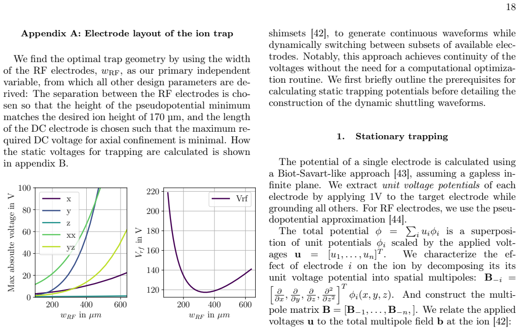
- RF electrode width wRF =
250 µm
- Ion height and waveguide depth x0 =
170 µm
- Glass block edge distance yg =
1 mm
- Stray-field scaling factor alpha =
2.05 ± 0.24
- Stray-field offsets E_o =
(-0.01, -0.10, 1.23) ± (0.04, 0.05, 0.09) V/mm
- Inferred surface charge density =
2.05 ± 0.24 e/µm2
- Mean phonon number in Rabi fit =
23.6 ± 2.2
assumptions (6)
- domain assumption Gapless infinite-plane approximation for electrode unit potentials
- domain assumption Pseudopotential approximation for the RF field
- ad hoc to paper Uniform surface charge density on all exposed glass surfaces
- ad hoc to paper Spatially constant background stray-field offsets
- standard math Thermal Boltzmann phonon distribution for the Rabi flop
- domain assumption Dielectric heating at 1 mm is negligible per the model of Ref. 39
Cite this review
Pith. "Pith review of Ion trap on borosilicate substrate with integrated femtosecond-laser-written waveguide." pith.science (2026). https://pith.science/paper/D672NSNQ
@misc{pith2026260813207,
  author       = {Pith},
  title        = {Pith review of: Ion trap on borosilicate substrate with integrated femtosecond-laser-written waveguide},
  year         = {2026},
  howpublished = {\url{https://pith.science/paper/D672NSNQ}},
  note         = {Machine review of arXiv:2608.13207}
}
abstract
We present an ion-trap platform on borosilicate glass with an integrated femtosecond-laser-written waveguide for on-chip light delivery. The optical layer is physically separated from the electrode substrate and bonded atop the trap, remaining compatible with silicon-based integration. We engineer single-mode low-loss guidance at 729 nm with tunable mode-field diameter and achieve low-loss curved waveguides down to a radius of curvature of 6 mm. We also extend single-mode operation to a wavelength of 405 nm. The fabrication process is compatible with the industrial fabrication of a single-metal-layer surface-electrode trap, including active fiber alignment and bonding. We validate the platform in a cryogenic trapped-ion system with $^{40}$Ca$^+$, demonstrating trapping, shuttling the ion to a zone in front of the waveguide, and coherent operations driven by 729 nm light delivered through the integrated waveguide. We characterize the effect of the exposed dielectric on the ion and measure stray electric fields that show slow drift at a timescale of hours. The architecture is compatible with hybrid micro-optics (e.g. pick-and-place lenses) to realize single ion addressing and provides a robust, scalable route to integrated light delivery for trapped-ion devices.
Figures


Figures from the paper (21 more)





Reference graph
Works this paper leans on
-
[1]
Spherical aberration as a process parameter Spherical aberration arising from refractive index mis- match during focusing into transparent substrates de- pends on the writing depth and leads to a distortion of the focal volume [25], which can significantly influence the resulting waveguide properties [26, 27]. We employ a microscope objective with adjusta...
-
[2]
Writing strategies for mode size tuning During process development, an extensive parameter space was explored, including variations in pulse dura- tion, repetition rate, polarization, numerical aperture, beam overfilling, writing speed, number of overscans, and correction collar position. An optimized parame- ter set was identified to achieve robust, low-...
-
[3]
Far-field divergence versus mode size In the presented experiments, the trapped ions are ad- dressed via the waveguide’s far-field emission, we inves- tigated how the mode-field diameter affects the far-field characteristics of the emitted beam by measuring the di- vergenceofwaveguideswithdifferentmodesizes. Smaller 7 160 170 180 190 200 Pulse energy in n...
-
[4]
Bending loss versus mode size Themode-fielddiameternotonlydeterminesthediver- gence of the emitted beam but also strongly influences the sensitivity of a waveguide to bending-induced loss, i.e., radiation losses arising from curvature of the propa- gationpath. Largeropticalmodesextendfurtherintothe surrounding lower-index material and are therefore more s...
-
[5]
Single-mode guiding at 405 nm Single-modewaveguidingoverawiderangeofthespec- trum is of particular relevance for integrated ion trap quantum processors, where laser light in the blue and vi- olet spectral range is commonly used for Doppler cooling, state preparation, and fluorescence readout of trapped ions. Integrating such wavelengths in on-chip photoni...
-
[6]
Electrode geometry The electronic layout of the trap features segmented electrodes for static potentials as well as RF electrodes to generate the ponderomotive pseudopotential. All metal structures on this device (electrodes, bond pads, and leads) are patterned within a single layer to reduce fab- rication complexity. The segmented DC electrodes are posit...
-
[7]
Optically In- tegrated Quantum Computing (OptoQuant)
Influence of the dielectric on the trapping potential The electrode structure of the trap was designed with- out the borosilicate glass block containing the waveguide. Now, we analyzed the effect of the optics block onto the RF trapping field with a Finite-Element Method (FEM). We model the trap substrate as borosilicate glass with a thickness of525µmand ...
-
[8]
Stationary trapping The potential of a single electrode is calculated using a Biot-Savart-like approach [43], assuming a gapless in- finite plane. We extractunit voltage potentialsof each electrode by applying1Vto the target electrode while grounding all others. For RF electrodes, we use the pseu- dopotential approximation [44]. The total potentialϕ= P iu...
Show all 54 references
-
[9]
Waveforms for shuttling We express the axial position of the ion during shut- tling with the dimensionless parameterξ(x) =x/(w dc + 19 wgap)relative to the segmented DC electrodes.ξ= 0de- notes the center of electrode pair 1 (see Fig. 7). Shuttling waveforms are generated by s...
-
[10]
tickling
Atξ= 4, pair 2 is swapped for pair 6.).Dashed lines: Continuous voltage waveforms achieved after the linear inter- polation and projection smoothing process. We generate continuous waveforms by defining a set of nodesN= [N 1,...,N m]where electrode switching oc- curs. For each...
-
[11]
C. D. Bruzewicz, J. Chiaverini, R. McConnell, and J. M. Sage, Trapped-ion quantum computing: Progress and challenges, Applied Physics Reviews6, 021314 (2019)
2019
-
[12]
Wang, C.-Y
P. Wang, C.-Y. Luan, M. Qiao, M. Um, J. Zhang, Y. Wang, X. Yuan, M. Gu, J. Zhang, and K. Kim, Single ion qubit with estimated coherence time exceeding one hour, Nature Communications12, 233 (2021)
2021
-
[13]
A. C. Hughes, R. Srinivas, C. M. Löschnauer, H. M. Knaack, R. Matt, C. J. Ballance, M. Malinowski, T. P. Harty, and R. T. Sutherland, Trapped-ion two-qubit gates with>99.99% fidelity without ground-state cool- ing (2025), arXiv:2510.17286 [quant-ph]
2025
-
[14]
M. C. Smith, A. D. Leu, K. Miyanishi, M. F. Gely, and D. M. Lucas, Single-qubit gates with errors at the10−7 level, Phys. Rev. Lett.134, 230601 (2025)
2025
-
[15]
Ransford, M
A. Ransford, M. S. Allman, J. Arkinstall, J. P. C. III, S. F. Cooper, R. D. Delaney, J. M. Dreiling, B. Estey, C. Figgatt, A. Hall, A. A. Husain, A. Isanaka, C. J. Kennedy, N. Kotibhaskar, I. S. Madjarov, K. Mayer, A. R. Milne, A. J. Park, A. P. Reed, R. Ancona, M. P. Andersen...
2025 arXiv
-
[16]
Pogorelov, T
I. Pogorelov, T. Feldker, C. D. Marciniak, L. Postler, G. Jacob, O. Krieglsteiner, V. Podlesnic, M. Meth, V. Negnevitsky, M. Stadler, B. Höfer, C. Wächter, K. Lakhmanskiy, R. Blatt, P. Schindler, and T. Monz, Compact ion-trap quantum computing demonstrator, PRX Quantum2, 020343 (2021)
2021
-
[17]
Proctor, K
T. Proctor, K. Young, A. D. Baczewski, and R. Blume- Kohout, Benchmarking quantum computers, Nature Re- views Physics7, 105 (2025)
2025
-
[18]
Kielpinski, C
D. Kielpinski, C. Monroe, and D. J. Wineland, Architec- ture for a large-scale ion-trap quantum computer, Nature 417, 709 (2002)
2002
-
[19]
J. M. Pino, J. M. Dreiling, C. Figgatt, J. P. Gaebler, S. A. Moses, M. S. Allman, C. H. Baldwin, M. Foss-Feig, D. Hayes, K. Mayer, C. Ryan-Anderson, and B. Neyen- huis, Demonstration of the trapped-ion quantum ccd computer architecture, Nature592, 209 (2021)
2021
-
[20]
Malinowski, D
M. Malinowski, D. Allcock, and C. Ballance, How to wire a1000-qubit trapped-ion quantum computer, PRX Quantum4, 040313 (2023)
2023
-
[21]
R. J. Niffenegger, J. Stuart, C. Sorace-Agaskar, D. Kha- ras, S. Bramhavar, C. D. Bruzewicz, W. Loh, R. T. Max- son, R. McConnell, D. Reens, G. N. West, J. M. Sage, and J. Chiaverini, Integrated multi-wavelength control of an ion qubit, Nature586, 538 (2020)
2020
-
[22]
K. K. Mehta, C. D. Bruzewicz, R. McConnell, R. J. Ram, J. M. Sage, and J. Chiaverini, Integrated optical addressing of an ion qubit, Nature Nanotechnology11, 1066 (2016)
2016
-
[23]
Badawi, P
B. Badawi, P. C. Holz, M. Raffetseder, N. Jungwirth, J. Ulmanis, H.-J. Quenzer, D. Kähler, T. Monz, and P. Schindler, Chiplet technology for large-scale trapped- ion quantum processors (2025), arXiv:2512.02645 [quant- ph]
2025
-
[24]
Momenzadeh, K
M. Momenzadeh, K. Sun, Q. Wu, B. You, Y.-L. Tang, H. Häffner, and M. R. Shcherbakov, Individual trapped- ion addressing with adjoint-optimized multimode pho- tonic circuits, npj Nanophotonics3, 3 (2026)
2026
-
[25]
K. K. Mehta, C. Zhang, M. Malinowski, T.-L. Nguyen, M. Stadler, and J. P. Home, Integrated optical multi-ion quantum logic, Nature586, 533 (2020)
2020
-
[26]
S. M. Eaton, M. L. Ng, R. Osellame, and P. R. Her- man, High refractive index contrast in fused silica waveg- uidesbytightlyfocused, high-repetitionratefemtosecond laser, Journal of Non-Crystalline Solids357, 2387 (2011), 17th International Symposium on Non-Oxide and New Optic...
2011
-
[27]
B. Guan, R. P. Scott, C. Qin, N. K. Fontaine, T. Su, C.Ferrari, M.Cappuzzo, F.Klemens, B.Keller, M.Earn- shaw, and S. J. B. Yoo, Free-space coherent optical com- munication with orbital angular, momentum multiplex- ing/demultiplexing using a hybrid 3d photonic integrated circu...
2014
-
[28]
Grüneberg, J
M. Grüneberg, J. Pribošek, A. Llobera, A. Zesar, J. Wahl, M. Preidl, Y. Colombe, K. Schüppert, C. Rössler, P. Hurdax, B. Lamprecht, and M. Mon- tagnese, On-chip laser beam delivery for integrated ion traps, in2023 22nd International Conference on Solid- State Sensors, Actuator...
2023
-
[29]
Auchter, C
S. Auchter, C. Axline, C. Decaroli, M. Valentini, L. Pur- win, R. Oswald, R. Matt, E. Aschauer, Y. Colombe, 22 P. Holz, T. Monz, R. Blatt, P. Schindler, C. Rössler, and J. Home, Industrially microfabricated ion trap with 1 ev trap depth, Quantum Science and Technology7, 035015 (2022)
2022
-
[30]
J. Ari, Y. Heng, M. Cavillon, M. Bernier, M. Dussauze, and M. Lancry, Overview of laser imprinted refractive in- dex changes and related thermal stability in mid-infrared optical glasses, Optical Materials163, 116985 (2025)
2025
-
[31]
A. W. Snyder and J. D. Love,Optical Waveguide Theory (Chapman and Hall, London, 1983)
1983
-
[32]
J. Li, E. Ertorer, and P. R. Herman, Ultrafast laser burst- train filamentation for non-contact scribing of optical glasses, Optics Express27, 25078 (2019)
2019
-
[33]
A.E.Siegman,Howto(maybe)measurelaserbeamqual- ity, inDPSS (Diode Pumped Solid State) Lasers: Appli- cations and Issues(Optica Publishing Group, 1998) p. MQ1
1998
-
[34]
D. Tan, X. Sun, Q. Wang, P. Zhou, Y. Liao, and J. Qiu, Fabricating low loss waveguides over a large depth in glass by temperature gradient assisted femtosecond laser writing, Optics Letters45, 3941 (2020)
2020
-
[35]
Hnatovsky, R
C. Hnatovsky, R. S. Taylor, E. Simova, V. R. Bhardwaj, D. M. Rayner, and P. B. Corkum, High-resolution study of photoinduced modification in fused silica produced by a tightly focused femtosecond laser beam in the presence of aberrations, Journal of Applied Physics98, 013517 (2005)
2005
-
[36]
Huang, P
L. Huang, P. S. Salter, F. Payne, and M. J. Booth, Aber- ration correction for direct laser written waveguides in a transverse geometry, Optics Express24, 10565 (2016)
2016
-
[37]
Bisch, J
N. Bisch, J. Guan, M. J. Booth, and P. S. Salter, Adaptive optics aberration correction for deep direct laser written waveguides in the heating regime, Applied Physics A125, 364 (2019)
2019
-
[38]
P. H. D. Ferreira, G. F. B. Almeida, and C. R. Mendonça, A simple strategy for increasing optical waveguide per- formance using spherical aberration, Optics and Laser Technology142, 107235 (2021)
2021
-
[39]
S. M. Eaton, M. L. Ng, J. Bonse, A. Mermillod-Blondin, H. Zhang, A. Rosenfeld, and P. R. Herman, Low-loss waveguides fabricated in bk7 glass by high repetition rate femtosecond fiber laser, Applied Optics47, 2098 (2008)
2008
-
[40]
S. M. Eaton, H. Zhang, M. L. Ng, J. Li, W.-J. Chen, S. Ho, and P. R. Herman, Transition from thermal dif- fusion to heat accumulation in high repetition rate fem- tosecond laser writing of buried optical waveguides, Op- tics Express16, 9443 (2008)
2008
-
[41]
W.-J. Chen, S. M. Eaton, H. Zhang, and P. R. Herman, Broadband directional couplers fabricated in bulk glass with high repetition rate femtosecond laser pulses, Optics Express16, 11470 (2008)
2008
-
[42]
Marcuse, Gaussian approximation of the fundamen- tal modes of graded-index fibers, Journal of the Optical Society of America68, 103 (1978)
D. Marcuse, Gaussian approximation of the fundamen- tal modes of graded-index fibers, Journal of the Optical Society of America68, 103 (1978)
1978
-
[43]
Marcuse, Curvature loss formula for optical fibers, Journal of the Optical Society of America66, 216 (1976)
D. Marcuse, Curvature loss formula for optical fibers, Journal of the Optical Society of America66, 216 (1976)
1976
-
[44]
Arriola, S
A. Arriola, S. Gross, N. Jovanovic, N. Charles, P. G. Tuthill, S. M. Olaizola, A. Fuerbach, and M. J. Withford, Low bend loss waveguides enable compact, efficient 3d photonic chips, Optics Express21, 29785 (2013)
2013
-
[45]
I. V. Dyakonov, S. A. Vetchinnikov, and A. A. Lipovskii, Low-loss single-mode integrated waveguides in soda-lime glass, Optics Letters41, 4498 (2016)
2016
-
[46]
Y. Wang, L. Zhong, K. Y. Lau, X. Han, Y. Yang, J. Hu, S. Firstov, Z. Chen, Z. Ma, L. Tong, K. S. Chiang, D. Tan, and J. Qiu, Precise mode control of laser-written waveguides for broadband, low-dispersion 3d integrated optics, Light: Science & Applications13, 31 (2024)
2024
-
[47]
Ross-Adams, B
A. Ross-Adams, B. Mills, M. J. Withford, and S. Gross, Low bend loss, high index, composite morphology ultra- fast laser written waveguides for photonic integrated cir- cuits, Light: Advanced Manufacturing5, 9 (2024)
2024
-
[48]
Anmasser, M
F. Anmasser, M. A. Zahra, K. Schüppert, M. Po- totschnig, J. Wahl, M. Dietl, M. Pfeifer, Y. Colombe, J.Repp, M.Brandl, P.Schindler,andC.Rössler,Demon- stration of a multiplexing trapped ion quantum process- ing unit (2026), arXiv:2605.16010 [quant-ph]
2026 arXiv
-
[49]
Teller, D
M. Teller, D. A. Fioretto, P. C. Holz, P. Schindler, V. Messerer, K. Schüppert, Y. Zou, R. Blatt, J. Chi- averini, J. Sage, and T. E. Northup, Heating of a trapped ion induced by dielectric materials, Phys. Rev. Lett.126, 230505 (2021)
2021
-
[50]
Freund, C
R. Freund, C. D. Marciniak, and T. Monz, A self- referenced optical phase noise analyzer for quantum tech- nologies, Review of Scientific Instruments95, 063005 (2024)
2024
-
[51]
Leibfried, R
D. Leibfried, R. Blatt, C. Monroe, and D. Wineland, Quantum dynamics of single trapped ions, Rev. Mod. Phys.75, 281 (2003)
2003
-
[52]
D. T. C. Allcock, J. A. Sherman, D. N. Stacey, A. H. Bur- rell, M. J. Curtis, G. Imreh, N. M. Linke, D. J. Szwer, S. C. Webster, A. M. Steane, and D. M. Lucas, Imple- mentation of a symmetric surface-electrode ion trap with field compensation using a modulated raman effect, Ne...
2010
-
[53]
M. H. Oliveira and J. A. Miranda, Biot-savart-like law in electrostatics,EuropeanJournalofPhysics22,31(2001)
2001
-
[54]
Dehmelt, Radiofrequency spectroscopy of stored ions i: Storage**part ii: Spectroscopy is now scheduled to appear in volume v of this series
H. Dehmelt, Radiofrequency spectroscopy of stored ions i: Storage**part ii: Spectroscopy is now scheduled to appear in volume v of this series. (Academic Press, 1968) pp. 53–72
1968
Reviewed August 15, 2026 · model on record in the stance chip above.
Discussion (0). Continue with ORCID to comment.