REVIEW 4 major objections 4 minor 20 references
Analog circuits for mixed-signal neuromorphic computing architectures in 28 nm FD-SOI technology
T0 review · 4 major / 4 minor · reviewed 2026-08-14 · deepseek-v4-flash
Pith's one-line read Bio-physically realistic synapse and neuron dynamics can be implemented in 28 nm FD-SOI with ultra-low-power analog circuits that cancel channel leakage and operate on pico-ampere currents.
desk verdict Solid 28nm FD-SOI synapse/neuron design with real engineering, but the leakage-cancellation claim needs measured data or a tighter analysis. read the letter →
The pith
A machine-rendered reading of the paper's core claim, the machinery that carries it, and where it could break.
The reading
What carries the argument
The load-bearing mechanism is a combination of leakage-canceling current subtraction and split-transistor sub-threshold biasing. The leakage-canceling block makes a scaled 4-to-1 copy of the 16 leak cells that mimic the 64 synapse blocks, sums their dark currents, and mirrors the result to subtract it from the total synapse current. The split-transistor pseudo-cascode technique, applied throughout the mirror transistors, keeps currents in the pico-ampere range with accurate mirroring despite advanced-node leakage and short-channel effects. Together these allow the Differential Pair Integrator and neuron compartments to realize long time constants with small MIMCAPs (1 pF and 1.5 pF) and compact active areas (3 $µm^{2}$ per synapse block, 20 $µm^{2}$ per neuron).
What would settle it
On the taped-out chip, drive all 256 synapse branches with zero input spikes and measure the summed output current before and after leakage cancellation while sweeping temperature over the operating range; if the post-cancellation baseline drifts by more than the intended pA-nA signal, the replica-matching assumption fails. A second check is to compare the measured synapse-neuron transfer function for 100 Hz input pulses with the simulated response shown in the paper.
Extended reading notes
Core claim
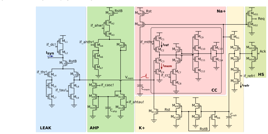
The central discovery is that compact sub-threshold synapse and neuron circuits can be built in 28 nm FD-SOI by treating leakage not as an unavoidable obstacle but as a current that can be replicated and subtracted. A 4-to-1 replica of 16 leak cells, biased with the same settings as the 64 synapse blocks (256 branches), produces a copy of the total dark current; this copy is subtracted from the summed synaptic current, leaving only the weighted signal. Synaptic dynamics are implemented with a Differential Pair Integrator whose time constants are set by a 1 pF MIMCAP and pico-ampere bias currents generated with split-transistor pseudo-cascode mirrors. The neuron, built from leak, after-hyperpolarization, sodium, and potassium compartments with a current comparator, occupies 20 $µm^{2}$ and produces spiking behaviors tunable from biologically plausible firing to fast ReLU-like transfer functions.
Load-bearing premise
The whole pico-ampere operating range rests on the assumption that the leakage current of 16 leak cells is a faithful 4-to-1 miniature of the leakage from the 64 synapse blocks (256 branches), so that subtracting its copy removes the real dark current under actual bias, temperature, and mismatch conditions.
Editorial extensions
If this is right
- A 64-synapse block with leakage cancellation can sum currents from 256 branches while keeping the output proportional to the true weighted input.
- The same circuits can be configured for slow, biologically realistic dynamics (tens to hundreds of milliseconds) for real-time sensory processing, and for fast ReLU-like transfer functions for spiking deep networks.
- Because the neuron and synapse blocks are compact, multi-core architectures can avoid time-multiplexing and memory transfer, bypassing the von Neumann bottleneck.
- The circuits are compatible with existing spike-based learning circuits and can be integrated into next-generation multi-neuron, multi-core neuromorphic processors.
Reading between the lines
- If the leakage replica tracks mismatch and temperature the same way in silicon, the same cancellation scheme should port to other advanced nodes where off-state leakage is the bottleneck, not just 28 nm FD-SOI.
- A natural next measurement is a chip-level comparison of the replica leak current against the 256-branch sum across temperature; that would quantify how much of the pA-nA operating range survives real silicon mismatch.
- The ReLU-like fast configuration suggests the same analog front end could be used for high-throughput event-driven deep networks, where the limiting factor becomes the AER encoder bandwidth rather than the synapse time constant.
Signed reviews
Editorial analysis
A structured set of objections, weighed in public.
Referee Report
Summary. The paper presents analog sub-threshold synapse and neuron circuits designed for a 28 nm FD-SOI process, intended for large-scale mixed-signal neuromorphic systems. The synapse circuit combines 64 programmable blocks (256 current branches) with a replica-based leakage-canceling block, a DPI low-pass filter for synaptic dynamics, an NMDA-like gating block, and a pA-nA current-mode integrator. The neuron circuit is a current-mode integrate-and-fire design with leak, AHP, Na+, and K+ compartments. The paper reports transistor-level simulation results for synaptic currents, membrane traces, and combined synapse-neuron transfer functions in both slow, biologically realistic regimes and fast ReLU-like regimes. The central claim is that leakage-canceling and mismatch-reducing techniques allow compact, energy-efficient pA-nA analog computation and millisecond-range time constants in an advanced scaled process.
Significance. If validated, this work would be a valuable demonstration that sub-threshold neuromorphic building blocks can be ported to 28 nm FD-SOI while retaining the long time constants and low currents needed for real-time sensory processing. The paper gives concrete area figures (3 µm^2 synapse block, 12.5 µm^2 DPI circuit, 20 µm^2 neuron), reports two clearly different operating regimes, and grounds the dynamics in the authors' prior DPI theory and measured 65 nm chip. The simulation traces are internally consistent with expected synaptic and neural dynamics. However, the load-bearing leakage-cancellation scheme rests on an unverified replica-matching assumption, and all reported results are simulations rather than measurements from the taped-out chip.
major comments (4)
- [Section II, Fig. 1] The leakage-cancellation scheme assumes that the summed dark current of a 4-to-1 replica of 16 leak cells (64 branches) matches the summed off-channel leakage of the 256 synapse branches. The paper provides no Monte Carlo, process-corner, or temperature analysis of this replica match. In 28 nm FD-SOI subthreshold operation, threshold-voltage mismatch causes exponential variation in leakage current, so the residual after subtraction may be comparable to the pA-scale signals the design targets. Please provide a mismatch/corner analysis of the replica relative to the synapse array and quantify the residual leakage after cancellation.
- [Section II, Fig. 1] The replica appears to be static: the leak cells are always dark, while a synapse branch that receives a presynaptic spike is active and no longer contributes its off-channel leakage. The fixed subtraction therefore over-cancels by approximately one dark-branch leakage current for each simultaneously active branch. The paper does not quantify this activity-dependent offset or explain how "the same leakage current" is maintained when branches are activated. This should be analyzed and, if necessary, corrected in the cancellation scheme.
- [Section III] All quantitative results in Figs. 4-6 are transistor-level simulation traces. The abstract and introduction mention that a chip has been taped out, but no measured leakage-cancellation accuracy, no measured time constants, and no simulation-versus-silicon comparison are reported. Since the central claim concerns pA-nA operation and long time constants in this specific process, measured validation of the leakage cancellation and subthreshold dynamics is needed to fully support the claim as stated.
- [Section II, Fig. 1] The text states that the Leakage Canceling block "attempts to produce the same leakage current," which correctly flags that matching is not guaranteed by construction. The subsequent simulation results implicitly assume ideal matching. The paper should either derive the matching requirement from device statistics and bias tolerances, or explicitly state the conditions under which the cancellation remains valid.
minor comments (4)
- [Section III] Figure 3 is referenced in the text but never discussed; its caption "Membrane current trace over time" lacks context, axis units, and simulation conditions. Please add a proper description.
- [Section II] The notation "dpi_tau!" and "dpi_thr!" appears with inconsistent formatting in the text and figure captions; please make the "!" convention for programmable biases uniform throughout.
- [Section II] The DPI time-constant dependence is described only qualitatively as proportional to capacitance and inversely proportional to the bias current. An explicit equation, or a reference to the exact formula in [17], would make the design trade-off reproducible.
- [Section II, Fig. 1] The phrase "4-to-1 copy of 16 leak cells with 4 branches each" is confusing; clarify that the replica contains 64 branches total, i.e., one quarter of the 256 synapse branches, and state how the 4-to-1 scaling is implemented in the current mirror.
Circularity Check
No significant circularity: the paper's results are transistor-level simulations of new 28 nm circuits, not fitted or self-referential derivations.
full rationale
The paper's central claim is that the proposed synapse and neuron circuits implement sub-threshold dynamics with leakage cancellation in 28 nm FD-SOI. The supporting evidence is schematic-level circuit design and transistor-level simulation (Figs. 4-6), not a quantity fitted to a target. The leakage-canceling block is described as an attempt to reproduce and subtract the off-channel leakage of 256 branches using a 4-to-1 replica; this is a design assumption whose correctness is asserted by construction of the schematic, but no 'prediction' is derived from it and no fitted value is renamed as a result. The paper cites the authors' prior DPI model [17] and prior fabricated chip [7] for the expected dynamics and for configurability, but these citations are contextual: the simulations in this paper are presented directly and the cited prior work includes fabricated and measured systems. Even if the replica-matching assumption is unverified under mismatch or temperature variation, that is a correctness/robustness concern, not circularity. There is no equation in the paper whose output is identical to an input by definition, and no fitted parameter that is then called a prediction. The self-citations are not load-bearing in the sense required for a circularity finding.
Assumptions & free parameters
free parameters (1)
- Simulation bias settings (dpi_tau!, dpi_thr!, Iref, refractory period) =
Not reported in the manuscript
assumptions (4)
- domain assumption Sub-threshold MOSFET operation with exponential I-V characteristics in 28nm FD-SOI.
- domain assumption DPI circuit implements first-order low-pass synaptic dynamics with time constant proportional to C/I.
- ad hoc to paper Leakage current of 256 synapse branches is replicable by a scaled 4-to-1 copy of leak cells.
- domain assumption Split-transistor pseudo-cascode biasing generates stable pA bias currents in 28nm.
Cite this review
Pith. "Pith review of Analog circuits for mixed-signal neuromorphic computing architectures in 28 nm FD-SOI technology." pith.science (2026). https://pith.science/paper/2M3N4SFJ
@misc{pith2026190807874,
  author       = {Pith},
  title        = {Pith review of: Analog circuits for mixed-signal neuromorphic computing architectures in 28 nm FD-SOI technology},
  year         = {2026},
  howpublished = {\url{https://pith.science/paper/2M3N4SFJ}},
  note         = {Machine review of arXiv:1908.07874}
}
read the original abstract
Developing mixed-signal analog-digital neuromorphic circuits in advanced scaled processes poses significant design challenges. We present compact and energy efficient sub-threshold analog synapse and neuron circuits, optimized for a 28 nm FD-SOI process, to implement massively parallel large-scale neuromorphic computing systems. We describe the techniques used for maximizing density with mixed-mode analog/digital synaptic weight configurations, and the methods adopted for minimizing the effect of channel leakage current, in order to implement efficient analog computation based on pA-nA small currents. We present circuit simulation results, based on a new chip that has been recently taped out, to demonstrate how the circuits can be useful for both low-frequency operation in systems that need to interact with the environment in real-time, and for high-frequency operation for fast data processing in different types of spiking neural network architectures.
Figures


Figures from the paper (3 more)


Reference graph
Works this paper leans on
-
[1]
Neuromorphic electronic systems,
C. Mead, “Neuromorphic electronic systems,”Proceedings of the IEEE , vol. 78, no. 10, pp. 1629–36, 1990
work page 1990
-
[2]
Frontiers in neuromorphic engineering,
G. Indiveri and T. Horiuchi, “Frontiers in neuromorphic engineering,”Frontiers in Neuroscience , vol. 5, no. 118, pp. 1–2,
-
[3]
Memory and information processing in neuromorphic systems,
G. Indiveri and S.-C. Liu, “Memory and information processing in neuromorphic systems,”Proceedings of the IEEE , vol. 103, no. 8, pp. 1379–1397, 2015. [Online]. Available: http://ncs.ethz.ch/pubs/pdf/ Indiveri_Liu15.pdf
work page 2015
-
[4]
J. Backus, “Can programming be liberated from the von neumann style?: a functional style and its algebra of programs,”Communications of the ACM , vol. 21, no. 8, pp. 613–641, 1978. [Online]. Available: http://doi.acm.org/10.1145/359576.359579
arXiv 1978
-
[5]
Neurogrid: A mixed-analog-digital multichip system for large-scale neural simulations,
B. V. Benjamin, P. Gao, E. McQuinn, S. Choudhary, A. R. Chan- drasekaran, J. Bussat, R. Alvarez-Icaza, J. Arthur, P. Merolla, and K. Boahen, “Neurogrid: A mixed-analog-digital multichip system for large-scale neural simulations,”Proceedings of the IEEE , vol. 102, no. 5, pp. 699–716, 2014
work page 2014
-
[6]
S. Furber, F. Galluppi, S. Temple, and L. Plana, “The SpiNNaker project,” Proceedings of the IEEE , vol. 102, no. 5, pp. 652–665, May 2014
work page 2014
-
[7]
N. Qiao, H. Mostafa, F. Corradi, M. Osswald, F. Stefanini, D. Sumislawska, and G. Indiveri, “A re-configurable on-line learning spiking neuromorphic processor comprising 256 neurons and 128k synapses,” Frontiers in Neuroscience , vol. 9, no. 141,
-
[8]
Hierarchical address event routing for reconfigurable large-scale neuromorphic systems,
J. Park, T. Yu, S. Joshi, C. Maier, and G. Cauwenberghs, “Hierarchical address event routing for reconfigurable large-scale neuromorphic systems,”IEEE Transactions on Neural Networks and Learning Systems , pp. 1–15, 2016
work page 2016
Show all 20 references
-
[9]
A million spiking-neuron integrated circuit with a scalable communication network and interface,
P. A. Merolla, J. V. Arthur, R. Alvarez-Icaza, A. S. Cassidy, J. Sawada, F. Akopyan, B. L. Jackson, N. Imam, C. Guo, Y. Nakamura, B. Brezzo, I. Vo, S. K. Esser, R. Appuswamy, B. Taba, A. Amir, M. D. Flickner, W. P. Risk, R. Manohar, and D. S. Modha, “A million spiking-neuron i...
2014
-
[10]
S.-C. Liu, J. Kramer, G. Indiveri, T. Delbruck, and R. Douglas,Analog VLSI:Circuits and Principles . MIT Press, 2002. [Online]. Available: http://ncs.ethz.ch/pubs/pdf/Liu_etal02b.pdf 5
2002
-
[11]
Scaling mixed-signal neuromorphic processors to 28nm fd-soi technologies,
N. Qiao and G. Indiveri, “Scaling mixed-signal neuromorphic processors to 28nm fd-soi technologies,” inBiomedical Circuits and Systems Conference, (BioCAS), 2016 . IEEE, 2016, pp. 552–555. [Online]. Available: http://ncs.ethz.ch/pubs/pdf/QiaoIndiveri16.pdf
2016
-
[12]
A neuromorphic event-based neural recording system for smart brain-machine-interfaces,
F. Corradi and G. Indiveri, “A neuromorphic event-based neural recording system for smart brain-machine-interfaces,”Biomedical Circuits and Systems, IEEE Transactions on , vol. 9, no. 5, pp. 699–709, 2015. [Online]. Available: http://ncs.ethz.ch/pubs/pdf/Corradi_Indiveri15.pdf
2015
-
[13]
A bidirectional brain-machine interface featuring a neuromorphic hardware decoder,
F. Boi, T. Moraitis, V. De Feo, F. Diotalevi, C. Bartolozzi, G. Indiveri, and A. Vato, “A bidirectional brain-machine interface featuring a neuromorphic hardware decoder,”Frontiers in Neuroscience, vol. 10, p. 563, 2016. [Online]. Available: http://journal.frontiersin.org/arti...
2016
-
[14]
Neuromorphic architectures for spiking deep neural networks,
G. Indiveri, F. Corradi, and N. Qiao, “Neuromorphic architectures for spiking deep neural networks,” inElectron Devices Meeting (IEDM), 2015 IEEE International . IEEE, Dec. 2015, pp. 4.2.1–4.2.14. [Online]. Available: http://ncs.ethz.ch/pubs/pdf/Indiveri_etal15.pdf
2015
-
[15]
Obstacle avoidance and target acquisition for robot navigation using a mixed signal analog/digital neuromorphic processing system,
M. B. Milde, H. Blum, A. Dietmüller, H. Blum, D. Sumislawska, J. Conradt, G. Indiveri, and Y. Sandamirskaya, “Obstacle avoidance and target acquisition for robot navigation using a mixed signal analog/digital neuromorphic processing system,”Frontiers in Neuroscience, 2017
2017
-
[16]
Addressable current reference array with 170db dynamic range,
M. Yang, S.-C. Liu, C. Li, and T. Delbruck, “Addressable current reference array with 170db dynamic range,” inCircuits and Systems (ISCAS), 2012 IEEE International Symposium on . IEEE, 2012, pp. 3110–3113
2012
-
[17]
Synaptic dynamics in analog VLSI,
C. Bartolozzi and G. Indiveri, “Synaptic dynamics in analog VLSI,” Neural Computation, vol. 19, no. 10, pp. 2581–2603, Oct 2007. [Online]. Available: http://ncs.ethz.ch/pubs/pdf/Bartolozzi_Indiveri07.pdf
2007
-
[18]
Compensation of CMOS op-amps using split-length transistors,
V. Saxena and R. J. Baker, “Compensation of CMOS op-amps using split-length transistors,” inCircuits and Systems (MWSCAS), 2008 IEEE 51st International Midwest Symposium on . IEEE, 2008, pp. 109–112
2008
-
[2011]
Available: http://www.frontiersin.org/neuromorphic_ engineering/10.3389/fnins.2011.00118/full
[Online]. Available: http://www.frontiersin.org/neuromorphic_ engineering/10.3389/fnins.2011.00118/full
2011 arXiv
-
[2015]
Available: http://www.frontiersin.org/neuromorphic_ engineering/10.3389/fnins.2015.00141/abstract
[Online]. Available: http://www.frontiersin.org/neuromorphic_ engineering/10.3389/fnins.2015.00141/abstract
2015
Reviewed August 14, 2026 · model on record in the stance chip above.
Discussion (0). Continue with ORCID to comment.