REVIEW 3 major objections 5 minor 16 references
Automatic gain control of ultra-low leakage synaptic scaling homeostatic plasticity circuits
T0 review · 3 major / 5 minor · reviewed 2026-08-14 · deepseek-v4-flash
Pith's one-line read This paper presents a compact CMOS automatic-gain-control circuit that uses a 1.2-aA leakage current to achieve homeostatic synaptic scaling with time constants up to 25,000 seconds.
desk verdict A real CMOS homeostatic AGC circuit with an order-of-magnitude lower leakage claim, but the headline 25k-s / 1.2-aA numbers rest on an unmeasured parasitic-leakage assumption and a single unreported trace. read the letter →
The pith
A machine-rendered reading of the paper's core claim, the machinery that carries it, and where it could break.
The reading
What carries the argument
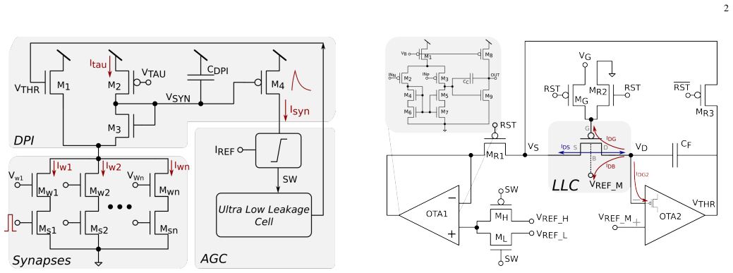
The argument is carried by two cooperating blocks. The first is the Differential-Pair Integrator (DPI) synapse, a log-domain integrator whose output current obeys $\tau_s \, dI_{\mathrm{syn}}/dt + I_{\mathrm{syn}} = I_w \, I_{\mathrm{gain}}/I_\tau$; here $I_w$ is the summed synaptic weight current and $I_{\mathrm{gain}}$ is an independent multiplicative scaling current set by a control voltage $V_{\mathrm{THR}}$, so scaling $I_{\mathrm{gain}}$ scales every afferent synapse together. The second is the ultra-low-leakage cell (LLC), a p-FET with $W/L = 0.5\,\mu\mathrm{m}/1\,\mu\mathrm{m}$ charging a 1 pF capacitor through a controllable current as small as 1.2 aA. Two subthreshold OTAs keep the drain-body voltage at zero and clamp the source voltage to one of two reference levels, while a comparator in the AGC loop chooses which reference is active; the result is a bang-bang loop that slowly raises or lowers $V_{\mathrm{THR}}$ until the DPI output current matches the reference $I_{\mathrm{REF}}$.
What would settle it
Set the cell to its slowest configuration, the one giving roughly 1.2 uV/s on the 1 pF capacitor, and record $V_{\mathrm{THR}}$ over an hour on multiple chips and at a range of temperatures; if the voltage ramp is not consistent with a 1.2-aA current, or if the firing-rate restoration time does not extend near 25,000 seconds, the central claim fails. Separately, measure $V_{DB}$ with the OTA2 feedback active to verify that it actually remains at zero.
Extended reading notes
Core claim
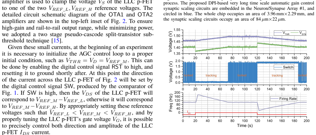
The central claim is that a single well-biased p-FET, with its drain-body voltage forced to zero by an on-chip feedback amplifier and its gate leakage contained below about 0.1 aA through transistor sizing, can produce a controllable current of around 1.2 aA. Charging or discharging a 1 pF capacitor with this current yields voltage slopes around 1.2 uV/s, which through the DPI synapse's exponential gain control slowly moves the neuron's firing rate back toward its set point. The paper demonstrates the full loop: after the input current steps from 0.3 nA to 0.6 nA and back, the neuron's firing rate rises and then returns to the reference 100 Hz over a tunable time constant, and the same setup reaches time scales of about 25,000 seconds in further tests.
Load-bearing premise
The load-bearing premise is that every unintended leakage path in the low-leakage transistor is smaller than about 0.1 atto-ampere, so the intended 1.2-aA control current is not drowned out; if the feedback amplifier cannot hold the drain-body voltage at zero, or the gate leakage is larger than estimated, the 25,000-second time constants will not reproduce.
Editorial extensions
If this is right
- Neuromorphic arrays can implement homeostatic plasticity on-chip in standard CMOS, avoiding floating-gate transistors and external digital storage.
- Because the loop scales all synapses afferent to a neuron through a shared $V_{\mathrm{THR}}$, relative synaptic weights are preserved during homeostasis, so learning-induced weight ratios are not disrupted.
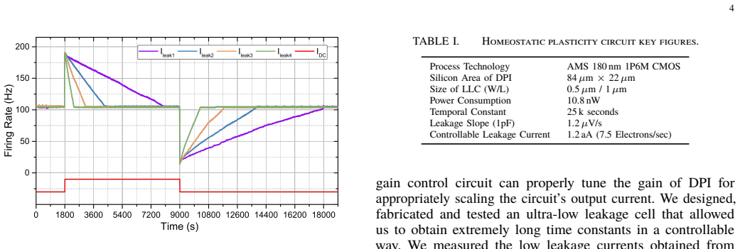
- The time constant is tunable by setting $V_G$ and the $V_{\mathrm{REF}}$ differences; the paper demonstrates restoration at roughly 60 seconds and verifies settings reaching about 25,000 seconds.
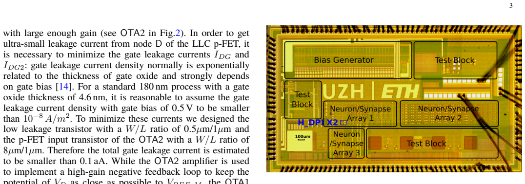
- A full homeostatic loop occupies 84 um by 22 um and consumes about 10.8 nW at 1.8 V, making it practical to embed in large neural arrays.
- The circuit restores the neuron's average firing rate to its reference value after bidirectional step changes in input drive, as shown by the 0.3 nA to 0.6 nA and back experiment.
Reading between the lines
- If the same leakage levels hold across process and temperature, the cell is a general-purpose analog integrator or memory: it could store a voltage for hours and drive other slow adaptive circuits, not just synaptic scaling.
- The bang-bang controller could be replaced by a linear or delta-sigma analog loop to reduce ripple near steady state; the paper's measurements show an alternating locked region where the comparator keeps toggling near equilibrium.
- A natural test is to combine this AGC with spike-timing-dependent plasticity in a small network: the multiplicative form of the scaling preserves weight ratios, so the two mechanisms should coexist; the paper motivates this but does not demonstrate it.
- With a larger capacitor or further leakage reduction, time constants could extend beyond 25,000 seconds toward days, approaching the hours-to-days scales of biological homeostatic plasticity.
Signed reviews
Editorial analysis
A structured set of objections, weighed in public.
Referee Report
Summary. The manuscript proposes an automatic gain control (AGC) circuit for homeostatic synaptic scaling in neuromorphic systems. The circuit uses a Differential Pair Integrator (DPI) synapse whose gain Igain is controlled by a voltage VTHR. A feedback loop compares the synaptic current to a reference and, via a comparator, switches a low-leakage cell (LLC) that slowly charges or discharges a 1 pF capacitor to adjust VTHR. The LLC is based on a subthreshold p-FET with leakage reduction techniques. The circuit was fabricated in 180 nm CMOS and occupies 84 µm × 22 µm with 10.8 nW power consumption. Measurements show closed-loop restoration of firing rate after step changes in the DPI input current (Fig. 4) and tunable restoration time scales up to about 9k seconds (Fig. 5). The paper further claims time constants up to 25k seconds and a controllable leakage current of 1.2 aA (7.5 electrons/s), inferred from a 1.2 µV/s slope on the 1 pF capacitor.
Significance. The ability to implement homeostatic plasticity with extremely long time constants in standard CMOS, without floating gates or off-chip digital control, is a valuable result for neuromorphic engineering. The measured closed-loop homeostasis (Fig. 4) is a direct demonstration of the AGC concept, and the area and power numbers are attractive. The paper also benefits from using standard, well-characterized subthreshold circuits (DPI, OTA) and from providing a concrete measurement method for leakage current. However, the headline 25k s and 1.2 aA claims are not fully substantiated by the presented data, so the significance is conditional on the additional evidence requested below.
major comments (3)
- [Section IV, after Fig. 5] The paper states that 'the longest time scale we measured in this experiment is around 9k seconds' and that 'we verified, with further tests' a time scale of about 25k seconds, but no waveform, trial count, or temperature is shown for the 25k s case. Since the 25k s value is the headline claim of the abstract and Table I, the authors should show the closed-loop firing-rate restoration (or at least the VTHR/VSYN trace) at that timescale and report the number of repetitions and conditions. Without this, the 25k s value is anecdotal rather than a measured result.
- [Section III, 'The ultra-low leakage cell'] The estimate that total gate leakage is smaller than 0.1 aA is derived from a gate-oxide leakage density taken from [14] and the device geometries, but it is an assumption, not a measurement. It also does not account for other parallel leakage paths into the CF node, such as OTA2 input leakage, drain-bulk junction leakage if the finite OTA2 gain leaves VDB slightly off zero, or capacitor and switch leakage. The inference in Section IV that the measured 1.2 µV/s slope corresponds to a controlled LLC channel current of 1.2 aA is only valid if these parasitic leakages are negligible. I recommend an explicit control measurement, e.g., monitoring the CF drift with the LLC p-FET channel forced off, to bound the parasitic leakage.
- [Section IV, Figs. 4 and 5] The measurements are reported without error bars, repeated trials, or temperature information; subthreshold leakage currents are exponentially sensitive to temperature and bias. To support the reproducibility of the reported time constants, the authors should specify the number of chips/devices measured, the ambient temperature, and the spread of the results.
minor comments (5)
- [Section IV, first paragraph] 'refectory period' should be 'refractory period'.
- [Section III and Table I] There are minor formatting issues ('with aW/L ratio', '10− 8A/m2') and the relationship between the 84 µm × 22 µm area, the DPI, and the LLC sizes should be clarified.
- [Throughout] The term 'time constant' is used inconsistently: Fig. 4 reports ~60 s, Fig. 5 up to ~9k s, and Table I lists 25k s. Define how each time constant is extracted (e.g., exponential fit to the firing-rate envelope, or VTHR ramp duration) so that the values are comparable.
- [Section I, discussion of prior work] The paper claims an improvement over the prior LLC in [8], but the discussion is brief; a short quantitative comparison (e.g., leakage current, time constant, area) would help the reader assess the novelty.
- [Section II, AGC loop description] In the description of the AGC loop, the comparator output SW is described as digital, but no hysteresis or deadband is mentioned; given the bang-bang behavior visible in Fig. 4, a sentence on comparator hysteresis (or its absence) would be useful.
Circularity Check
No significant circularity: the AGC loop, ultra-low leakage cell, and reported time constants rest on direct circuit measurements and standard external device-physics references, not on fitted or self-referential definitions.
full rationale
The paper's central claims are empirical rather than derived from fitted inputs or self-referential definitions. The DPI transfer function (Eq. 1) and the Igain expression (Eq. 2) are taken from prior published circuit analyses ([11], [12]) and are used as design equations; the target results, namely AGC restoration of the firing rate, the 1.2 aA leakage current, and the 25 ks time scale, are obtained from direct measurements of VTHR, VSYN, and SW, together with the elementary calculation i = C dV/dt using the measured 1.2 µV/s slope on the 1 pF capacitor. The LLC gate-leakage bound of <0.1 aA is estimated from an external device-physics source [14] and is not fitted to the 1.2 aA value, so the leakage-current claim does not reduce to its own input. The 'further tests' yielding 25 ks are not documented and the result assumes that parasitic leakages remain below the controlled current, but these are evidence-quality and reproducibility concerns, not circularity. Self-citations [8], [11], and [12] are prior work by the authors, but they are used as background and design tools, while the new chip measurements stand independently of those citations. No load-bearing step in the derivation chain is equivalent by construction to the paper's own outputs.
Assumptions & free parameters
assumptions (5)
- domain assumption Subthreshold MOSFET operation with exponential I-V relation and translinear principle apply to the DPI and LLC circuits.
- domain assumption The OTA2 feedback loop forces VDB = 0, eliminating drain-bulk leakage in the LLC p-FET.
- domain assumption Gate leakage current density is below 1e-8 A/m^2 at 0.5 V gate bias for the 180nm process, so total gate leakage is <0.1 aA.
- domain assumption The DPI synapse circuit model of Eq. (1) from references [11,12] is accurate for the fabricated chip.
- standard math The capacitor equation I = C dV/dt holds for the 1 pF capacitor CF.
Cite this review
Pith. "Pith review of Automatic gain control of ultra-low leakage synaptic scaling homeostatic plasticity circuits." pith.science (2026). https://pith.science/paper/4Z4VVJE4
@misc{pith2026190807412,
  author       = {Pith},
  title        = {Pith review of: Automatic gain control of ultra-low leakage synaptic scaling homeostatic plasticity circuits},
  year         = {2026},
  howpublished = {\url{https://pith.science/paper/4Z4VVJE4}},
  note         = {Machine review of arXiv:1908.07412}
}
read the original abstract
Homeostatic plasticity is a stabilizing mechanism that allows neural systems to maintain their activity around a functional operating point. This is an extremely useful mechanism for neuromorphic computing systems, as it can be used to compensate for chronic shifts, for example due to changes in the network structure. However, it is important that this plasticity mechanism operates on time scales that are much longer than conventional synaptic plasticity ones, in order to not interfere with the learning process. In this paper we present a novel ultra-low leakage cell and an automatic gain control scheme that can adapt the gain of analog log-domain synapse circuits over extremely long time scales. To validate the proposed scheme, we implemented the ultra-low leakage cell in a standard 180 nm Complementary Metal-Oxide-Semiconductor (CMOS) process, and integrated it in an array of dynamic synapses connected to an adaptive integrate and fire neuron. We describe the circuit and demonstrate how it can be configured to scale the gain of all synapses afferent to the silicon neuron in a way to keep the neuron's average firing rate constant around a set operating point. The circuit occupies a silicon area of 84 {\mu}m x 22 {\mu}m and consumes approximately 10.8 nW with a 1.8 V supply voltage. It exhibits time constants of up to 25 kilo-seconds, thanks to a controllable leakage current that can be scaled down to 1.2 atto-Amps (7.5 electrons/s).
Figures
Figures from the paper (1 more)
Reference graph
Works this paper leans on
-
[14]
W. K. Henson, N. Yang, S. Kubicek, E. M. Vogel, J. J. Wortman, K. De Meyer, and A. Naem, “Analysis of leakage currents and impact on off-state power consumption for CMOS technology in the 100-nm regime,”Electron Devices, IEEE Transactions on , vol. 47, no. 7, pp. 1393–1400, 2000
work page 2000
-
[1]
Synaptic depression and the temporal response characteristics of V1 cells,
F. Chance, S. Nelson, and L. Abbott, “Synaptic depression and the temporal response characteristics of V1 cells,”The Journal of Neuroscience, vol. 18, no. 12, pp. 4785–99, 1998
work page 1998
-
[2]
Synaptic plasticity: taming the beast,
L. Abbott and S. Nelson, “Synaptic plasticity: taming the beast,”Nature Neuroscience, vol. 3, pp. 1178–1183, November 2000
work page 2000
-
[3]
Homeostatic plasticity in the developing nervous system,
G. Turrigiano and S. Nelson, “Homeostatic plasticity in the developing nervous system,”Nature Reviews Neuroscience , vol. 5, pp. 97–107, February 2004
work page 2004
-
[4]
Homeostatic plasticity in neural networks: the more things change, the more they stay the same,
G. Turrigiano, “Homeostatic plasticity in neural networks: the more things change, the more they stay the same,”Trends in Neuroscience, vol. 22, no. 5, pp. 221–227, 1999
work page 1999
-
[5]
Homeostasis in a silicon integrate-and-fire neuron,
S.-C. Liu and B. Minch, “Homeostasis in a silicon integrate-and-fire neuron,” inAdvances in Neural Information Processing Systems (NIPS) , T. Leen, T. Dietterich, and V. Tresp, Eds., vol. 13. MIT Press, 2001, pp. 727–733
work page 2001
-
[6]
Floating-gate-based intrinsic plasticity with low-voltage rate control,
S. Nease and E. Chicca, “Floating-gate-based intrinsic plasticity with low-voltage rate control,” inInternational Symposium on Circuits and Systems ISCAS 2014. IEEE, 2016, pp. 2507–2510
work page 2014
-
[7]
Implementing homeostatic plasticity in VLSI networks of spiking neurons,
C. Bartolozzi, O. Nikolayeva, and G. Indiveri, “Implementing homeostatic plasticity in VLSI networks of spiking neurons,” in International Conference on Electronics, Circuits, and Systems, ICECS
Show all 16 references
-
[8]
Ultra low leakage synaptic scaling circuits for implementing homeostatic plasticity in neuromorphic architectures,
G. Rovere, N. Qiao, C. Bartolozzi, and G. Indiveri, “Ultra low leakage synaptic scaling circuits for implementing homeostatic plasticity in neuromorphic architectures,” inInternational Symposium on Circuits and Systems, (ISCAS), 2014 . IEEE, 2014, pp. 2073–2076
2014
-
[9]
Leak- age current mechanisms and leakage reduction techniques in deep- submicrometer CMOS circuits,
K. Roy, S. Mukhopadhyay, and H. Mahmoodi-Meimand, “Leak- age current mechanisms and leakage reduction techniques in deep- submicrometer CMOS circuits,”Proceedings of the IEEE , vol. 91, no. 2, pp. 305–327, 2003. 5
2003
-
[10]
A 10-nw 12-bit accurate analog storage cell with 10-aa leakage,
M. O’Halloran and R. Sarpeshkar, “A 10-nw 12-bit accurate analog storage cell with 10-aa leakage,”Solid-State Circuits, IEEE Journal of , vol. 39, no. 11, pp. 1985–1996, 2004
1985
-
[11]
Synaptic dynamics in analog VLSI,
C. Bartolozzi and G. Indiveri, “Synaptic dynamics in analog VLSI,” Neural Computation, vol. 19, no. 10, pp. 2581–2603, Oct 2007
2007
-
[12]
Neuromorphic electronic circuits for building autonomous cognitive systems,
E. Chicca, F. Stefanini, C. Bartolozzi, and G. Indiveri, “Neuromorphic electronic circuits for building autonomous cognitive systems,” Proceedings of the IEEE , vol. 102, no. 9, pp. 1367–1388, Sep 2014
2014
-
[13]
A re-configurable on-line learning spiking neuromorphic processor comprising 256 neurons and 128k synapses,
N. Qiao, H. Mostafa, F. Corradi, M. Osswald, F. Stefanini, D. Sumislawska, and G. Indiveri, “A re-configurable on-line learning spiking neuromorphic processor comprising 256 neurons and 128k synapses,”Frontiers in Neuroscience, vol. 9, no. 141, 2015
2015
-
[15]
Subthreshold DC-gain enhance- ment by exploiting small size effects of MOSFETs,
M. Yang, S.-C. Liu, and T. Delbruck, “Subthreshold DC-gain enhance- ment by exploiting small size effects of MOSFETs,”Electronics Letters, vol. 50, no. 11, pp. 835–837, 2014
2014
-
[2008]
IEEE, 2008, pp. 682–685
2008
Reviewed August 14, 2026 · model on record in the stance chip above.
Discussion (0). Continue with ORCID to comment.