Dislocation-templated antiferromagnetic domains in epitaxial NiO
Pith reviewed 2026-06-27 02:21 UTC · model grok-4.3
The pith
Interface dislocation networks pin antiferromagnetic domain walls at identical nanoscale locations in epitaxial NiO
A machine-rendered reading of the paper's core claim, the machinery that carries it, and where it could break.
Core claim
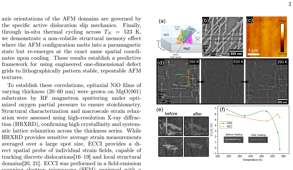
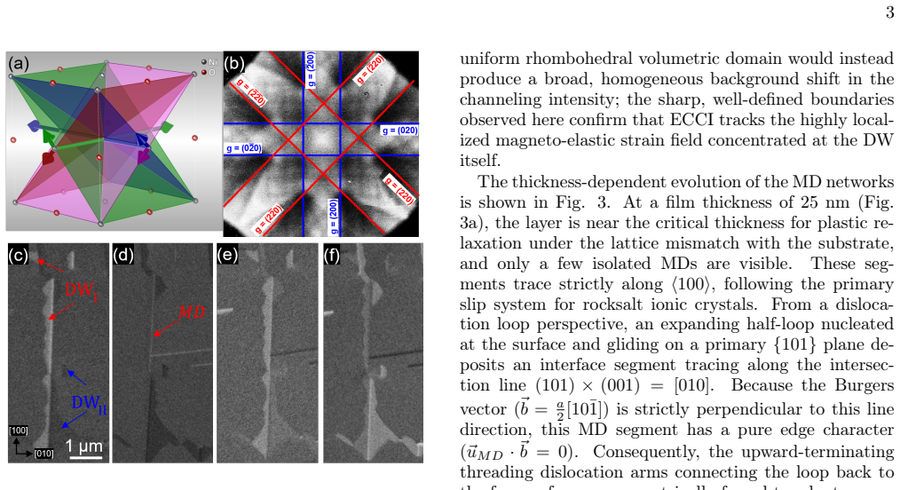
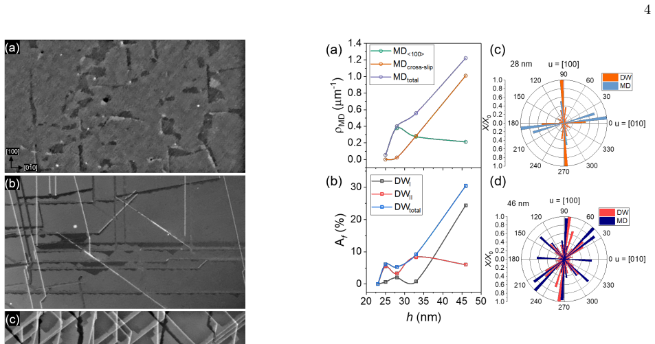
Antiferromagnetic twin-domain walls are deterministically pinned at the nanoscale by interface dislocation networks in epitaxial NiO/MgO(001), as demonstrated by their re-emergence at identical spatial locations after thermal cycling across the Neel temperature, with domain contrast arising from localized rhombohedral magnetostrictive strain fields and quantitative image analysis showing that domain wall area fractions directly track the density and configuration of the evolving misfit dislocation networks.
What carries the argument
interface misfit dislocation networks that evolve with film thickness and template the pinning of antiferromagnetic twin-domain walls through localized strain fields
If this is right
- Domain wall patterns follow the density and spatial arrangement of misfit dislocation networks across different film thicknesses.
- Strain relaxation begins with interface misfit dislocations along <100> and transitions to zig-zag networks along <110> at larger thicknesses via cross-slip.
- Domain contrast originates from rhombohedral magnetostrictive strain localized at the domain walls.
- This approach supplies a framework for engineering antiferromagnetic textures using controlled one-dimensional defects.
Where Pith is reading between the lines
- Controlling growth parameters to shape the dislocation network could produce predetermined antiferromagnetic domain configurations for device applications.
- The same pinning effect may appear in other epitaxial antiferromagnets where magnetostriction couples domains to lattice defects.
- Mechanical or electrical perturbations could be tested to see if they can displace the walls while the underlying dislocation template remains fixed.
Load-bearing premise
The re-emergence of domain-wall contrast at identical spatial locations after thermal cycling is caused by pinning from the evolving misfit dislocation networks rather than by other unmentioned structural features or by the imaging method itself.
What would settle it
Domain walls failing to reappear at the same locations after thermal cycling in a sample where the dislocation network has been independently removed or altered would falsify the deterministic pinning claim.
Figures
read the original abstract
Controlling antiferromagnetic domains is essential for spintronics, yet deterministic manipulation remains challenging due to their lack of net magnetization. Here, we utilize scanning electron microscopy electron channeling contrast imaging (ECCI) to demonstrate a robust structural memory effect in epitaxial NiO/MgO(001), where antiferromagnetic twin-domain walls (DWs) are deterministically pinned at the nanoscale by interface dislocation networks. Thermal cycling across the Neel temperature reveals that while DW contrast completely vanishes in the paramagnetic phase, the features re-emerge at identical spatial locations upon cooling. Diffraction-vector-dependent ECCI demonstrates that domain contrast stems from localized rhombohedral magnetostrictive strain fields. By tracking a film thickness series from 23 to 60 nm, we resolve an explicit transition in oxide relaxation mechanics. A primary slip system initiates strain relaxation via interface misfit dislocations (MDs) tracking along <100>. At greater thicknesses, rising critical strain prompts threading segments to cross-slip onto secondary or higher-index planes, depositing a wavy network of zig-zag MD lines deviated toward <110>. Quantitative image analysis reveals that DW area fractions directly track the local density and spatial configuration of the evolving MD networks, providing a framework for defect-engineering antiferromagnetic textures using one-dimensional defects.
Editorial analysis
A structured set of objections, weighed in public.
Referee Report
Summary. The manuscript reports ECCI observations on epitaxial NiO/MgO(001) films claiming that antiferromagnetic twin-domain walls are deterministically pinned at the nanoscale by evolving interface misfit dislocation networks. Evidence includes complete vanishing of DW contrast above TN followed by re-emergence at identical locations upon cooling, diffraction-vector dependence linking contrast to rhombohedral magnetostrictive strain, and quantitative tracking of DW area fractions with MD density/configuration across a 23–60 nm thickness series that shows a transition from <100> to zig-zag <110>-deviated MD networks.
Significance. If the pinning interpretation is substantiated with additional controls, the result would establish a practical route for defect-engineering of antiferromagnetic textures via one-dimensional interface defects, which is relevant for spintronic control of AF order. The thickness-dependent shift in relaxation slip systems also adds to the literature on strain relaxation in rock-salt oxides.
major comments (2)
- [Abstract] Abstract: the central claim that DWs are 'deterministically pinned' by MD networks rests on spatial registry after thermal cycling, yet the text supplies no error bars, raw data, statistical tests, or full methods for the quantitative image analysis that asserts DW area fractions 'directly track' MD density; this renders the correlation unverifiable.
- [Abstract] Abstract: the interpretation that re-emergent DW contrast coincides specifically with MD locations (rather than other fixed structural features such as substrate steps or ECCI contrast mechanisms) is not supported by explicit exclusion experiments or additional characterization; diffraction-vector dependence confirms the strain origin but does not demonstrate spatial coincidence with the MD networks.
Simulated Author's Rebuttal
We thank the referee for the careful review and constructive comments. We address each major comment point by point below, indicating where revisions will be made to strengthen the manuscript.
read point-by-point responses
-
Referee: [Abstract] Abstract: the central claim that DWs are 'deterministically pinned' by MD networks rests on spatial registry after thermal cycling, yet the text supplies no error bars, raw data, statistical tests, or full methods for the quantitative image analysis that asserts DW area fractions 'directly track' MD density; this renders the correlation unverifiable.
Authors: We agree that the abstract would benefit from additional detail on the quantitative analysis to enhance verifiability. The full manuscript describes the image analysis in the Methods section, including how DW area fractions were extracted from ECCI images. To address this concern directly, we will revise the abstract to briefly note the analysis approach and error estimation, and we will add explicit references to supplementary raw data and statistical tests in the main text. revision: yes
-
Referee: [Abstract] Abstract: the interpretation that re-emergent DW contrast coincides specifically with MD locations (rather than other fixed structural features such as substrate steps or ECCI contrast mechanisms) is not supported by explicit exclusion experiments or additional characterization; diffraction-vector dependence confirms the strain origin but does not demonstrate spatial coincidence with the MD networks.
Authors: The spatial registry is supported by the re-emergence of contrast at identical locations after thermal cycling across TN, combined with the quantitative correlation of DW area fractions to the evolving MD density and configuration across the thickness series. The diffraction-vector dependence establishes the rhombohedral strain origin. While dedicated exclusion experiments for alternatives such as substrate steps were not performed, the thickness-dependent transition in MD networks (from <100> to zig-zag <110>) and the corresponding change in DW patterns provide evidence against static substrate features. We will add a clarifying discussion paragraph to explicitly rule out alternative interpretations using the existing data. revision: partial
Circularity Check
No circularity: purely experimental observations with no derivations or fitted inputs
full rationale
The manuscript is an experimental report relying on direct ECCI imaging, thermal cycling across TN, diffraction-vector dependence, and a thickness series (23-60 nm) to observe DW re-emergence and correlation with MD networks. No equations, ansatzes, fitted parameters, or derivation chains are present in the provided text. Claims rest on image analysis and spatial registry rather than any reduction to prior results by construction. Self-citations, if present, serve only as background and are not load-bearing for the reported measurements.
Axiom & Free-Parameter Ledger
axioms (1)
- domain assumption NiO undergoes a paramagnetic transition above its Neel temperature, allowing domain contrast to vanish and reappear
Reference graph
Works this paper leans on
-
[1]
Baltz, A
V. Baltz, A. Manchon, M. Tsoi, T. Moriyama, T. Ono, and Y. Tserkovnyak, Reviews of Modern Physics90, 015005 (2018)
2018
-
[2]
Jungwirth, X
T. Jungwirth, X. Marti, P. Wadley, and J. Wunderlich, Nature Nanotechnology11, 231 (2016)
2016
-
[3]
Cheong, M
S.-W. Cheong, M. Fiebig, W. Wu, L. Chapon, and V. Kiryukhin, npj Quantum Materials5, 3 (2020)
2020
-
[4]
Lebrun, A
R. Lebrun, A. Ross, O. Gomonay, V. Baltz, U. Ebels, A.-L. Barra, A. Qaiumzadeh, A. Brataas, J. Sinova, and M. Kläui, Nature Communications11, 6332 (2020)
2020
-
[5]
A. Ross, R. Lebrun, O. Gomonay, D. A. Grave, A. Kay, L. Baldrati, S. Becker, A. Qaiumzadeh, C. Ulloa, G. Jakob, F. Kronast, J. Sinova, R. Duine, A. Brataas, A. Rothschild, and M. Kläui, Nano Letters20, 306 (2020)
2020
-
[6]
Scholl, J
A. Scholl, J. Stöhr, J. Lüning, J. W. Seo, J. Fompeyrine, H. Siegwart, J.-P. Locquet, F. Nolting, S. Anders, E. E. Fullerton, M. R. Scheinfein, and H. A. Padmore, Science 287, 1014 (2000)
2000
-
[7]
Gross, W
I. Gross, W. Akhtar, V. Garcia, L. J. Martínez, S. Chouaieb, K. Garcia, C. Carrétéro, A. Barthélémy, P. Appel, P. Maletinsky, J.-V. Kim, J. Y. Chauleau, N. Jaouen, M. Viret, M. Bibes, S. Fusil, and V. Jacques, Nature549, 252 (2017)
2017
-
[8]
M. Bode, E. Y. Vedmedenko, K. von Bergmann, A. Ku- betzka, P. Ferriani, S. Heinze, and R. Wiesendanger, Na- ture Materials5, 477 (2006)
2006
-
[9]
M. A. James and T. Hibma, Surface Science433-435, 718 (1999)
1999
-
[10]
P. Gao, Physical Review Letters120, 10.1103/Phys- RevLett.120.267601 (2018)
-
[11]
Sugiyama, N
I. Sugiyama, N. Shibata, Z. Wang, S. Kobayashi, T. Ya- mamoto, and Y. Ikuhara, Nature Nanotechnology8, 266 (2013)
2013
-
[12]
W. L. Roth, Physical Review110, 1333 (1958)
1958
-
[13]
Yamada, Journal of the Physical Society of Japan21, 650 (1966)
T. Yamada, Journal of the Physical Society of Japan21, 650 (1966)
1966
-
[14]
Nakahigashi, N
K. Nakahigashi, N. Fukuoka, and Y. Shimomura, Journal of the Physical Society of Japan38, 1634 (1975)
1975
-
[15]
Mandal, K
S. Mandal, K. S. R. Menon, F. Maccherozzi, and R. Belkhou, Physical Review B80, 184408 (2009)
2009
-
[16]
J. T. Boyer, A. N. Blumer, Z. H. Blumer, D. L. Lep- kowski, and T. J. Grassman, Journal of Crystal Growth 571, 126251 (2021)
2021
-
[17]
B. B. Haidet, J. Meyer, P. Reddy, E. T. Hughes, and K. Mukherjee, Physical Review Materials7, 024602 (2023)
2023
-
[18]
H. Yan, E. Postelnicu, T. Nguyen, S. Corujeira Gallo, A. Stacey, and K. Mukherjee, Applied Physics Letters 124, 102108 (2024)
2024
-
[19]
Fonseca Montenegro, M
A. Fonseca Montenegro, M. Baan, M. Ghazisaeidi, T. J. Grassman, and R. C. Myers, Crystal Growth & Design 24, 6007 (2024)
2024
-
[20]
J. F. Ihlefeld, J. R. Michael, B. B. McKenzie, D. A. Scrymgeour, J.-P. Maria, E. A. Paisley, and A. R. Ki- tahara, Journal of Materials Science52, 1071 (2017)
2017
-
[21]
W. Peng, A. Singh, M. H. Qaiser, P. Fahler-Muenzer, F. Watson, L. Si, Y. Xie, K. E. Sopińska, D. A. Chaney, A. M. Sanchez, T. B. Britton, R. Beanland, M. Had- jimichael, and M. Alexe, Advanced Materials38, e15762 (2026)
2026
-
[22]
Moriyama, L
T. Moriyama, L. Sánchez-Tejerina, K. Oda, T. Ohkochi, M. Kimata, Y. Shiota, H. Nojiri, G. Finocchio, and T. Ono, Physical Review Materials7, 054401 (2023)
2023
-
[23]
Strunk, physica status solidi (a)28, 119 (1975)
H. Strunk, physica status solidi (a)28, 119 (1975)
1975
-
[24]
Narita, T
N. Narita, T. Yoshimura, Y. Takahara, and K. Higashida, Materials Transactions42, 41 (2001)
2001
discussion (0)
Sign in with ORCID, Apple, or X to comment. Anyone can read and Pith papers without signing in.