REVIEW 3 major objections 5 minor 69 references
Controlled spin-torque driven domain wall motion using staggered magnetic nanowires
T0 review · 3 major / 5 minor · reviewed 2026-08-14 · deepseek-v4-flash
Pith's one-line read This paper demonstrates that a staggered magnetic nanowire lets current pulses position a domain wall at precise, reproducible steps, making depinning current and thermal stability tunable by geometry.
desk verdict Real geometric pinning and stepwise DW motion, but the paper's central claim that this is spin-transfer torque is not supported by the reported experiments. read the letter →
The pith
A machine-rendered reading of the paper's core claim, the machinery that carries it, and where it could break.
The reading
What carries the argument
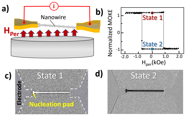
The central object is the staggered nanowire: a 1-$\mu$m-wide perpendicular-anisotropy wire with repeated lateral displacements, an offset $d$ in the y-direction and a step length $\lambda$ in the x-direction, that act as nanoconstrictions. Each constriction creates a local energy barrier, the pinning potential, for the domain wall; the barrier height is set by $d$ and $\lambda$, so which wall position is stable and what current is needed to depin it are engineered by the lithography. The measurement setup is polar MOKE imaging synchronized with pulsed current and perpendicular field, and the analysis uses a thermally activated time-to-depinning law, from which a thermal stability factor $S \approx 50$ is extracted. Micromagnetic simulation then connects the depinning current density to the uniaxial anisotropy $K_u$, showing that $J_{\mathrm{dep}}$ falls as $K_u$ decreases and changes with $\lambda$.
What would settle it
A concrete check is to repeat the step-to-step pulse protocol with reversed current polarity and with the magnetization direction of the device reversed; if the wall depins at the same current magnitude and moves the same way regardless of polarity, spin-transfer torque is not the driver, and a heating-only control would confirm whether temperature rise alone causes the displacement.
Extended reading notes
Core claim
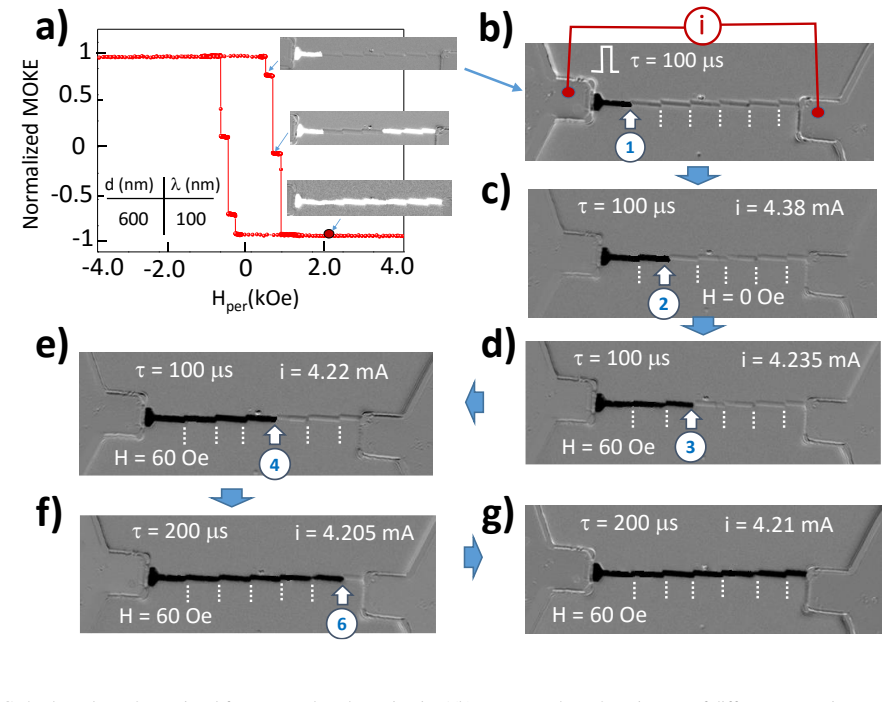
In a [Co(0.3 nm)/Ni(0.6 nm)]$_{12}$ multilayer with perpendicular magnetic anisotropy, the authors create 50-$\mu$m-long, 1-$\mu$m-wide nanowires with repeated lateral offsets, called steps. They show that a domain wall nucleated at a pad is held at the first step and can be pushed to the second step by a 100 $\mu$s current pulse of 4.38 mA at zero field; moving it to later steps requires currents near 4.2 mA at a fixed 60 Oe perpendicular assist field, and each position is reproducible and stable for hours. The minimum current for depinning, $i_{\mathrm{dep}}$, depends on the step dimensions: for $d = 600$ nm, $\lambda = 100$ nm it is larger and weakly field-dependent, while for $d = 200$ nm, $\lambda = 0$ it is smaller and decays exponentially with applied field. Micromagnetic calculations show the depinning current density $J_{\mathrm{dep}}$ can be tuned by changing $\lambda$ for fixed $d$, and the authors interpret the results as controlled spin-transfer-torque-driven motion enabled by the staggered design.
Load-bearing premise
The load-bearing premise is that the observed step-by-step displacement is caused by spin-transfer torque; the study does not report reversed-polarity or temperature control experiments that would rule out resistive heating or current-generated magnetic fields as the mover.
Editorial extensions
If this is right
- A racetrack-style memory could write bits at predetermined physical locations simply by choosing the number of pulses and the geometry of the steps, removing the uncertainty of where a domain ends up after propagation.
- The depinning current can be reduced without sacrificing long-term stability: the measured stability factor near 50 exceeds the level typically needed for years-long retention, so lower-anisotropy material can be used to drop $J_{\mathrm{dep}}$.
- Because different values of $d$ and $\lambda$ give different $i_{\mathrm{dep}}$ versus applied-field behavior, the same material system supports tunable pinning strength, enabling multi-level cells where each step is one stored state.
- The method applies to perpendicular-anisotropy (Co/Ni) multilayers already used in spin-torque devices, so it is compatible with existing STT-based writing and reading schemes.
Reading between the lines
- A decisive control experiment would flip current polarity, with the initial magnetization direction also reversed, while keeping the magnitude fixed; if the wall depins at the same current and moves the same way in both cases, the motion is not spin-torque driven, since STT is polarity-sensitive.
- The observed exponential drop of the depinning current with applied field for the shallower step resembles thermally activated depinning; measuring time-to-depinning at several temperatures would separate the intrinsic barrier from any current-induced heating and test the STT interpretation.
- If each step is engineered with a different offset $d$, the current threshold itself could encode information, allowing multi-level storage where the number of steps read out identifies the wall position; this is a natural extension the paper leaves implicit.
Signed reviews
Editorial analysis
A structured set of objections, weighed in public.
Referee Report
Summary. The manuscript describes stepped ("staggered") (Co/Ni) nanowires with perpendicular magnetic anisotropy in which lithographic offsets (d, λ) act as domain-wall pinning sites. Using polar MOKE imaging, the authors show that a domain wall initially stabilized at a step can be transferred to subsequent steps by pulsed current (about 4.2–4.4 mA, 100–200 μs), with a 60 Oe assisting field for the later steps, and that the resulting states are stable for hours. They measure depinning current versus perpendicular field for two geometries, fit depinning-time data with a Sharrock-type expression to obtain a stability factor S ≈ 50, and present micromagnetic calculations (from prior work) of depinning-current density versus anisotropy to support the tunability of the design.
Significance. If correct, the staggered-nanowire concept would be a practical fabrication-based route to deterministic domain-wall positioning in PMA racetrack-type devices, and the MOKE images directly document reproducible step-by-step displacement. The direct visualization and the hours-scale stability of the states are genuine strengths. The experimental demonstration is, however, qualitative: the current-induced mechanism is not isolated from thermal or Oersted-field effects, the two-device dataset is too small to establish the claimed geometry dependence, and the long-term stability statement is an extrapolation from an under-specified fit. These issues are addressable, so the work is a promising applied-physics contribution that needs revision rather than rejection.
major comments (3)
- [Section III, Figs. 4(c)-4(g)] The central claim that the observed domain-wall displacement is "spin-torque driven" is not established by the reported experiments. All depinning-current values in Fig. 4 appear to be of one polarity; there is no reversed-current control, no step-free nanowire control, and no measurement of sample temperature. Joule heating is polarity-even, and the 100–200 μs pulse widths are long enough for thermal steady state, so the step-to-step displacements observed with a 60 Oe assisting field in Figs. 4(d)-4(g) are equally consistent with thermally assisted depinning at the next constriction; Oersted-field effects are likewise not excluded. For STT in a perpendicular-anisotropy wire, reversing the current should reverse the expected propagation direction, while Joule heating does not, so a current-polarity reversal is a simple discriminating test. Because the title and abstract assert STT-driven motion, this missing control is load-bearing.
- [Section III, Fig. 5(a)] The quantitative claim that the depinning current idep depends on the stagger parameters d and λ rests on two devices, each shown as a single trace with no error bars, no device counts, and no statistics. The reported trends (nearly flat for d = 600 nm/λ = 100 nm versus exponential decay for d = 200 nm/λ = 0 nm) cannot be assessed for significance. The geometry labels are also inconsistent: the Fig. 5(a) inset lists black dots as d = 600 nm, λ = 100 nm, whereas the caption and text for Fig. 5(b) refer to a device with d = 600 nm and λ = 0 nm. Please specify the exact geometries of both panels and provide replication statistics.
- [Section III, Eqs. (1)-(3) and Fig. 5(b)] The thermal-stability claim is model-dependent and under-specified. The stability factor S is obtained by fitting Eq. (2) to the depinning-time data, but the attempt frequency f0 is not stated, the exponent α in Eq. (1) is free while Eq. (2) fixes it at 2/3, and no fit uncertainties or residuals are shown. The statement in Section III that the domain wall "will remain stable for more than 5 years" is an extrapolation from this fitted S and therefore does not provide independent evidence of long-term stability. Please report f0, justify applying Sharrock's law to domain-wall depinning, and show how S varies with the assumed attempt frequency.
minor comments (5)
- [Section III, Fig. 4] The pulse protocol is described inconsistently: the text says the pulse width is fixed at 100 μs, but Figs. 4(f) and 4(g) are labeled τ = 200 μs; please state the full protocol including polarity, pulse number, and synchronization with MOKE acquisition.
- [Section III, Fig. 2] The text refers to "nanowires shown in Fig. 2(d)", but Fig. 2 contains panels (a)-(c) only; this cross-reference appears to be an error.
- [Section III, Fig. 6] The vertical axis of Fig. 6 is labeled as Jdep in units of 10^11 J/m^2; the correct unit for a current density is A/m^2.
- [Section III] Reference [69] is cited as "To be published" in support of the claim that (Co/Pt) stepped devices pin DW at each step; a published reference or the corresponding data should be provided.
- [Abstract and Section III] The abstract states that the pinning potential was found to depend on device dimensions, but the manuscript reports no direct measurement of a pinning potential; please either provide such a measurement or reword the abstract.
Circularity Check
No significant circularity: central DW displacement is a direct MOKE observation, and the Sharrock fit and prior-work simulation are not load-bearing.
full rationale
The central claim of controlled domain-wall motion is established by direct MOKE imaging at specific pulsed currents (Fig. 4), not by a fit or by an equation that returns its own input. The depinning current idep is defined operationally and measured. The thermal stability factor S is obtained by fitting Eq. (2) to measured time-to-depinning data, and the statement that the DW could remain stable for more than five years is a standard Sharrock-type extrapolation from that fitted model; it is not a prediction of the same data points used in the fit, so it is not circular by construction. Fig. 6 cites the authors' prior work [61] for a micromagnetism calculation of Jdep versus Ku, but this is not load-bearing for the paper's central demonstration: the experimental Fig. 5(a) already shows the dependence of idep on d and lambda, and the summary does not require the simulation. The citation is a published prior result rather than an unverified uniqueness argument or ansatz. No fitted parameter is renamed as an independent prediction, no equation reduces to its definition, and no self-citation chain forces the result. Concerns about whether the motion is truly spin-torque-driven rather than thermally assisted are experimental-control issues (correctness risk), not circularity.
Assumptions & free parameters
free parameters (4)
- H0 =
not quoted
- B =
not quoted
- attempt frequency f0 (or tau0) =
assumed, not stated
- micromagnetic simulation parameters =
not given (from [61])
assumptions (3)
- domain assumption Sharrock's law applies to domain wall depinning in these nanostructures
- domain assumption The observed current-induced DW displacement is due to spin-transfer torque
- domain assumption Standard LLG/micromagnetic formalism from [61] is valid for this geometry
Cite this review
Pith. "Pith review of Controlled spin-torque driven domain wall motion using staggered magnetic nanowires." pith.science (2026). https://pith.science/paper/5IEU66PI
@misc{pith2026190809304,
  author       = {Pith},
  title        = {Pith review of: Controlled spin-torque driven domain wall motion using staggered magnetic nanowires},
  year         = {2026},
  howpublished = {\url{https://pith.science/paper/5IEU66PI}},
  note         = {Machine review of arXiv:1908.09304}
}
read the original abstract
The growing demand for storage, due to big data applications, cannot be met by hard disk drives. Domain wall (DW) memory devices such as racetrack memory offer an alternative route to achieve high capacity storage. In DW memory, control of domain wall positions and their motion using spin-transfer torque are important challenges. In this paper, we demonstrate controlled domain wall motion using spin-transfer torque in staggered magnetic nanowires. The devices, fabricated using electron-beam lithography, were tested using a magneto-optical Kerr microscopy and electrical transport measurements. The depinning current, pinning potential and thermal stability were found to depend on the device dimensions of the staggering nanowires. Thus, the proposed staggering configuration helps to fine-tune the properties of domain wall devices for memory applications.
Figures

Figures from the paper (1 more)
Reference graph
Works this paper leans on
-
[61]
M. Al Bahri, B. Borie, T.L. Jin, R. Sbiaa, M. Kläui, and S.N. Piramanayagam, Staggered magnetic nanowire devices for effective domain-wall pinning in racetrack memory, Phys. Rev. Appl. 11, 024023 (2019)
work page 2019
-
[1]
J. C. Slonczewski, Phys. Rev. B39, 6995 (1989)
work page 1989
-
[2]
Berger, Emission of spin waves by a magnetic multilayer traversed by a current
L. Berger, Emission of spin waves by a magnetic multilayer traversed by a current. Phys. Rev. B54, 9353 (1996)
work page 1996
-
[3]
J. A. Katine, F. J. Albert, R. A. Buhrman, E. B. Myers, and D. C. Ralph, Phys. Rev. Lett. 84, 3149 (2000)
work page 2000
-
[4]
J. Grollier, V. Cros, A. Hamzic, J. M. George, H. Jaffres, A. Fert, G. Faini, J. B. Youssef, and H. L. Gall, Spin- (nm) 100 d = 600 (nm) 200 4 5 6 7 8 10 12 14 16 18 Jdep (x10 11 J/m 2 ) Ku (x10 5 J/m 3 ) 9 polarized current induced switching in Co/Cu/Co pillars. Appl. Phys. Lett. 78, 3663 (2001)
work page 2001
-
[5]
S. I. Kiselev, J. C. Sankey, I. N. Krivorotov, N. C. Emley, R. J. Schoelkopf, R. A. Buhrman, and D. C. Ralph, Microwave oscillations of a nanomagnet driven by a spin polarized current, Nature (London) 425, 380 (2003)
work page 2003
- [6]
- [7]
Show all 69 references
-
[8]
Ikeda, K
S. Ikeda, K. Miura, H. Yamamoto , K. Mizunuma, H. D. Gan, M. Endo, S. Kanai, J. Hayakawa, F. Matsukura, and H. Ohno, A perpendicular -anisotropy CoFeB -MgO magnetic tunnel junction, Nature Mater. 9, 721(2010)
2010
-
[9]
Khalili Amiri , Z
P. Khalili Amiri , Z. M. Zeng, J. Langer, H. Zhao, G. Rowlands, Y.-J. Chen, I. N. Krivorotov, J. -P. Wang, H. W. Jiang, J. A. Katine, Y. Huai, K. Galatsis, and K. L. Wang, Switching current reduction using perpendicular anisotropy in CoFeB –MgO magnetic tunnel junctions. Appl....
2011
-
[10]
D. C. Worledge, G. Hu, David W. Abraham, J. Z. Sun, P. L. Trouilloud, J. Nowak, S. Brown, M. C. Gaidis, E. J. O’Sullivan, and R. P. Robertazzi, Appl. Phys. Lett. 98, 22501 (2011)
2011
-
[11]
H. Meng, R. Sbiaa, C. C. Wang, S. Y. H. Lua, and M. A. K. Akhtar, Annealing temperature window for tunneling magnetoresistance and spin torque switching in CoFeB/MgO/CoFeB perpendicular magnetic tunnel junctions, J. Appl. Phys. 110, 103915 (2011)
2011
-
[12]
C. C. Wang, M. A. K. Bin Akhtar, R. Sbiaa, H. Meng, L. Y. H. Sunny, S. K. Wong, L. Ping, P. Carlberg, and A. K. S. Arthur, Size Dependence effect in MgO-based CoFeB tunnel junctions with perpendicular magnetic anisotropy, Jpn. J. Appl. Phys. 51, 013101 (2012)
2012
-
[13]
H. Liu, D. Bedau, J. Z. Sun, S. Mangin, E. E. Fullerton, J. A. Katine, A. D. Kent, Dynamics of spin torque switching in all -perpendicular spin valve nanopillars, J. Magn. Magn. Mater. 358, 233 (2014)
2014
-
[14]
Bhatti, R
S. Bhatti, R. Sbiaa, A. Hirohata, H. Ohno, S. Fukami, and S.N.Piramanayagam, Spintronics based Random Access Memory: A Review, Mat. Today 20, 530 (2017)
2017
-
[15]
X. Chen, C. Zhou, Z. Zhang, J. Chen, X. Zheng, L. Zhang, C. M. Hu, and H. Guo, Enhancing the spin transfer torque in magnetic tunnel junctions by ac modulation, Phys. Rev. B95, 115417 (2017)
2017
-
[16]
W. H. Rippard, M. R. Pufall, S. Kaka, S. E. Russek, and T. J. Silva, Direct-current induced dynamics in Co90Fe10/Ni80Fe20 point contacts , Phys. Rev. Lett. 92, 027201 (2004)
2004
-
[17]
Kaka et al
S. Kaka et al. Mutual phase-locking of microwave spin torque nano-oscillators. Nature 437, 389–392 (2005)
2005
-
[18]
A. V. Nazarov et al., Spin transfer stimulated microwave emission in MgO magnetic tunnel junctions. Appl. Phys. Lett. 88, 162504 (2006)
2006
-
[19]
A. M. Deac et al. , Bias-driven high -power microwave emission from MgO -based tunnel magnetoresistance devices. Nat. Phys. 4, 803 (2008)
2008
-
[20]
Georges et al
B. Georges et al. , Coupling efficiency for phase locking of a spin transfer o scillator to a microwave curren, Phys. Rev. Lett. 101, 017201 (2008)
2008
-
[21]
Houssamedine et al., Spin transfer induced coherent microwave emission with large power from nanoscale MgO tunnel junctions , Appl
D. Houssamedine et al., Spin transfer induced coherent microwave emission with large power from nanoscale MgO tunnel junctions , Appl. Phys. Lett. 93, 022505 (2008)
2008
-
[22]
M. W. Keller, A. B. Kos, T. J. Silva, W. H. Rippard, and M. R. Pufall, Time domain measurement of phase noise in a spin torque oscillator. Appl. Phys. Lett. 94, 193105 (2009)
2009
-
[23]
Saida, and S
D. Saida, and S. Nakamura, Magnetization states of a spin- torque oscillator having perpendicular polarizer and planar free layer, J. Appl. Phys. 112, 083926 (2012)
2012
-
[24]
G. E. Rowlands, J. A. Katine, J. Langer, J. Zhu, and I. N. Krivorotov, Time domain mapping of spin torque oscillator effective energy. Phys. Rev. Lett. 111, 087206 (2013)
2013
-
[25]
Sbiaa, Frequency selection for magnetization switching in spin torque magnetic memory
R. Sbiaa, Frequency selection for magnetization switching in spin torque magnetic memory. J. Phys. D: Appl. Phys. 48, 195001 (2015)
2015
-
[26]
Wernsdorfer, B
W. Wernsdorfer, B. Doudin, D. Mailly, K. Hasselbach, A. Be noit, J. Meier, J. -Ph. Ansermet, and B. Barbara, 10 Nucleation of Magnetization Reversal in Individual Nanosized Nickel Wires, Phys. Rev. Lett. 77, 1873 (1996)
1996
-
[27]
Yamaguchi et al., Real-space observation of current - driven domain wall motion in submicron magnetic wires
A. Yamaguchi et al., Real-space observation of current - driven domain wall motion in submicron magnetic wires. Phys. Rev. Lett. 92, 077205 (2004)
2004
-
[28]
Zhang, and Z
S. Zhang, and Z. Li, Roles of nonequilibrium conduction electrons on the magnetization dynamics of ferromagnets. Phys. Rev. Lett. 93, 127204 (2004)
2004
-
[29]
D. A. Allwood, G. Xiong, C. C. Faulkner, D. Atkinson, D. Petit, and R. P. Cowburn, Magnetic Domain -Wall Logic, Science 309, 1688 (2005)
2005
-
[30]
Kläui, H
M. Kläui, H. Ehrke, U. Rüdiger, T. Kasama, R. E. Dunin- Borkowski, D. Backes, L. J. Heyderman, C. A. F. Vaz, J. A. C. Bland, G. Faini , E. Cambril, and W. Wernsdorfer, Direct observation of domain -wall pinning at nanoscale constrictions, Appl. Phys. Lett. 87, 102509 (2005)
2005
-
[31]
G. S. D. Beach, C. Nistor, C. Knutson, M. Tsoi, and J. L. Erskine, Dynamics of field -driven domain -wall propagation in ferromagnetic nanowires, Nature Mater. 4, 741 (2005)
2005
-
[32]
Thiaville, Y
A. Thiaville, Y. Nakatani, J. Miltat, and Y. Suzuki, Micromagnetic understanding of current -driven domain wall motion in patterned nanowires. Europhys. Lett. 69, 990 (2005)
2005
-
[33]
Hayashi, L
M. Hayashi, L. Thomas, C. Rettner, R. Moriya, X. Jiang, and S. S. P. Parkin, Dependence of Current and Field Driven Depinning of Domain Walls o n Their Structure and Chirality in Permalloy Nanowires, Phys. Rev. Lett. 97, 207205 (2006)
2006
-
[34]
Gubbiotti, S
G. Gubbiotti, S. Tacchi, G. Carlotti, N. Singh, S. Goolaup, A. O. Adeyeye, and M. Kostylev, Collective spin modes in monodimensional magnonic crystals consisti ng of dipolarly coupled nanowires, Appl. Phys. Lett. 90, 092503 (2007)
2007
-
[35]
S. S. P. Parkin, M. Hayashi, and L. Thomas, Magnetic Domain-Wall Racetrack Memory, Science 320, 190 (2008)
2008
-
[36]
O’Brien, D
L. O’Brien, D. E. Read, H. T. Zeng, E. R. Lewis, D. Petit, and R. P. Cowburn, Bidirectional magnetic nanowire shift register, Appl. Phys. Lett. 95, 232502 (2009)
2009
-
[37]
Diegel, S
M. Diegel, S. Glathe, R. Mattheis, M. Scherzinder, and E. Halder, A New Four Bit Magnetic Domain Wall Based Multiturn Counter, IEEE Trans. Magn. 45, 3792 (2009)
2009
-
[38]
T. H. E. Lahtinen, K. J. A. Franke, and S. van Dijken, Electric-field control of magnetic domain wall motion and local magnetization reversal, Sci. Rep. 2, 258 (2012)
2012
-
[39]
Brataas, Chiral domain walls move faster
A. Brataas, Chiral domain walls move faster. Nat. Nanotech. 8, 485 (2013)
2013
-
[40]
Tanigawa, T
H. Tanigawa, T. Suzuki, S. Fukami, K. Suemitsu, N. Ohshima, and E. Kariyada, Thickness dependence of current-induced domain wall motion in a Co/Ni multi - layer with out-of-plane anisotropy, Appl. Phys. Lett. 102, 152410 (2013)
2013
-
[41]
Fernandez -Pacheco, L
A. Fernandez -Pacheco, L. Serrano -Ramón, J. M. Michalik, M. R. Ibarra, J. M. De Teresa, L. O'Brien, D. Petit, J. Lee, and R. P. Cowburn, Three dimensional magnetic nanowires grown by focused electron -beam induced deposition, Sci. Rep. 3, 1492 (2013)
2013
-
[42]
Sbiaa, and S
R. Sbiaa, and S. N. Piramanayagam, Multi -level domain wall memory in constricted magnetic nanowires, Appl. Phys. A 114, 1347 (2014)
2014
-
[43]
Laurson, K
Van de Wiele, L. Laurson, K. J. A. Franke , and S. van Dijken, Electric field driven magnetic domain wall motion in ferromagnetic -ferroelectric heterostructures, Appl. Phys. Lett. 104, 012401 (2014)
2014
-
[44]
J.-S. Kim, M. -A. Mawass, A. Bisig, B. Krüger, R. M. Reeve, T. Schulz, F. Büttner, J. Yoon, C. -Y. You, M. Weigand, H. Stoll, G. Schütz, H. J. M. Swagten, B. Koopmans, S. Eisebitt, and M. Kläui, Synchronous precessional motion of multiple domain walls in a ferromagnetic nanowi...
2014
-
[45]
Sbiaa, and R
R. Sbiaa, and R. Chantrell, Domain wall oscillations induced by spin torque in magnetic nanowires. J. Appl. Phys. 117, 053907 (2015)
2015
-
[46]
Caretta et al
L. Caretta et al. , Fast current -driven domain walls and small skyrmions in a compensated ferrimagnet. Nat. Nanotechnol. https://doi.org/10.1038/s41565 -018-0255- 3 (2018)
2018 doi
-
[47]
Kim et al
K.-J. Kim et al. Fast domain wall motion in the vicinity of the angular momentum compensation temperature of ferrimagnets. Nat. Mater. 16, 1187 (2017). 11
2017
-
[48]
Sbiaa, R
R. Sbiaa, R. Law, S. Lua, E. L. Tan, T. Tahmasebi, C. C. Wang, and S. N. Piramanayagam, Appl. Phys. Lett. 99 092506 (2011)
2011
-
[49]
K. F. Huang, D. S. Wang, M. H. Tsai, H. H. Lin, and C.- H. Lai, Initialization-free multilevel states driven by spin- orbit torque switching, Adv. Mat. 29, 1601575 (2017). Three dimensional D multilevel spin transfer torque devices, Appl. Phys. Lett. 112, 112402 (2018)
2017
-
[50]
L. K. Bogart, D. Atkinson, K. O'Shea, D. McGrouther, and S. Mc Vitie, Dependence of domain wall pinning potential landscapes on domain wall chirality and pinning site geometry in planar nanowires, Phys. Rev B79, 054414 (2009)
2009
-
[51]
K. Xu, D. K. Schreiber, Y. L. Li, B. R. Johnson, and J. McCloy, Effect of defects, magnetocrystalline anisotropy, and shape anisotropy on magnetic structure of iron thin films by magnetic force microscopy, AIP Adv. 7, 056806 (2017)
2017
-
[52]
Castilla, M
D. Castilla, M. Maicas, J. L. Prieto, and M. P. J. Proenca, Depinning process of magnetic domain walls in cylindrical nanowires with a chemical constraint, J. Phys. D-Appl. Phys. 50,105001 (2017)
2017
-
[53]
Backes, C
D. Backes, C. Schieback, M. Kläui, F. Junginger, H. Ehrke, P. Nielaba, U. Rüdiger, L. J. Heyderman, C. S. Chen, T. Kasama, R. E. Dunin-Borkowski, C. A. F. Vaz, and J. A. C. Bland, Transverse domain walls in nanoconstrictions, Appl. Phys. Lett. 95, 112502 (2007)
2007
-
[54]
Petit, A
D. Petit, A. -V Jausovec, D. Read, and R. P. J. Cowburn, Domain wall pinning and potential landscapes created by constrictions and protrusions in ferromagnetic nanowires, J. Appl. Phys. 103, 114307 (2008)
2008
-
[55]
Huang and C
S.-H. Huang and C. -H. Lai, Domain-wall depinning by controlling its configuration at notch, Appl. Phys. Lett. 95, 032505 (2009)
2009
-
[56]
L. K. Bogart, D. Atk inson, K. O’Shea, D. McGrouther and S. McVitie, Dependence of domain wall pinning potential landscapes on domain wall chirality and pinning site geometry in planar nanowires, Phys. Rev. B79, 054414 (2009)
2009
-
[57]
Al Bahri and R
M. Al Bahri and R. Sbiaa, Geometrically pinned magnetic domain wall for multi -bit per cell storage memory, Sci. Rep. 6, 28590 (2016)
2016
-
[58]
Berganza, C
E. Berganza, C. Bran, M. Jaafar, M. Vázquez, and A. Asenjo, Domain wall pinning in FeCoCu bamboo -like nanowires, Sci. Rep. 6, 29702 (2016)
2016
-
[59]
A. Ding, I. Will, C. Lu and Y. B. Xu, Vortex domain wall formation in nanowires with twin pinning sites, IEEE Trans. Magn. 48, 2304 (2012)
2012
-
[60]
Y. Gao, B. You, X. Z. Ruan, M. Y. Liu, H. L. Yang, Q. F. Zhan, Z. Li, N. Lei, W. S. Zhao, D. F. Pan, J. G. Wan, J. Wu, H. Q. Tu, J. Wang, W. Zhang, Y. B. Xu, and J. Du, Depinning of domain walls in permalloy nanowires with asymmetric notches, Sci. Rep. 6, 32617 (2016)
2016
-
[62]
Polenciuc, A
I. Polenciuc, A. J. Vick, D. A. Allwood, T. J. Hayward, G. Vallejo-Fernandez, K. O'Grady, and A. Hirohata, Domain wall pinning for racetrack memory using exchange bias, Appl. Phys. Let. 105, 162406 (2014)
2014
-
[63]
T. Jin, F. Tan, C. Ang, W. Gan, J. Cao, W. S. Lew, and S.N. Piramanayagam, Tilted magnetisation for domain wall pinning in racetrack memory, J. Magn. Magn. Mater. 489, 165410 (2019)
2019
-
[64]
T. Jin, F. Tan, W. C. Law, W. Gan, I. Soldatov, R. Schäfer, C. Ma, X. Liu, W. S. Lew, and S.N. Piramanayagam, Nanoscale modification of magnetic properties for effective domain wall pinning, J. Magn. Magn. Mater. 475, 70 (2019)
2019
-
[65]
T. Jin, M. Ranjbar, S. He, W . C. Law, T. Zhou, W. S. Lew, X. Liu, and S.N. Piramanayagam, Tuning magnetic properties for domain wall pinning via localized metal diffusion, Sci. Rep. 7, 16208 (2017)
2017
-
[66]
T. Jin, D. Kumar, W. Gan, M. Ranjbar, F. Luo, R. Sbiaa, X. Liu, W. S. Lew, and S.N. Piramanayagam, Nanoscale compositional modification in Co/Pd multilayers for controllable domain wall pinning in racetrack memory, Phys. Status Solidi RRL 12, 1800197 (2018)
2018
-
[67]
Kumar, T
D. Kumar, T. Jin, S. Al -Risi, R. Sbiaa, W. S. Lew, and S.N. Piramanayagam, Domain wall motion control for racetrack memory applications, IEEE Trans. Magn . 55, 2300708 (2018). 12
2018
-
[68]
Al Subhi , and R
A. Al Subhi , and R. Sbiaa, Control of magnetization reversal and domain structure in (Co/Ni) multilayers, J. Magn. Magn. Mater. 489, 165460 (2019)
2019
-
[70]
M. P. Sharrock, Time dependence of switching fields in magnetic recording media, J. Appl. Phys.76, 6413 (1994)
1994
Reviewed August 14, 2026 · model on record in the stance chip above.
Discussion (0). Continue with ORCID to comment.