REVIEW 3 major objections 7 minor 41 references
Tunable anisotropic behaviors in phosphorene under periodic potentials in arbitrary directions
T0 review · 3 major / 7 minor · reviewed 2026-08-14 · deepseek-v4-flash
Pith's one-line read A periodic potential stripe rotated over a phosphorene monolayer can tune its electronic anisotropy, effective mass, and optical absorption, with absorption changing by more than an order of magnitude.
desk verdict A useful angle-dependent superlattice study of phosphorene, but the defining potential profile is internally inconsistent, so the quantitative maps and the order-of-magnitude absorption claim need to be redone or explicitly justified. read the letter →
The pith
A machine-rendered reading of the paper's core claim, the machinery that carries it, and where it could break.
The reading
What carries the argument
The engine of the calculation is a two-band $\mathbf{k}\cdot\mathbf{p}$ Hamiltonian for monolayer phosphorene built from $D_{2h}$ symmetry, with parameters fitted to the conduction and valence bands. Rotating the coordinate system so that one axis lies along the periodic potential transforms the band parameters into angle-dependent coefficients $\alpha'_{c,v} = \alpha \cos^2\theta + \beta \sin^2\theta$, $\beta'_{c,v} = \alpha \sin^2\theta + \beta \cos^2\theta$, and a cross term $\lambda = (-\alpha+\beta)\sin\theta\cos\theta$, which is how the stripe orientation enters every later result. The periodic potential is taken as $U(x)=V_0\cos(2\pi x/W)$ with stripe width $W=10$ nm and period $L=20$ nm, and the electron wave function is expanded in plane waves with periodic boundary conditions, yielding mini-bands whose curvature defines the effective mass. Optical absorption is computed from the transition rate between valence and conduction mini-bands using the dipole interaction $H_{\mathrm{int}}=\gamma(e/\hbar)A_x$, integrated over $k$ space, with a broadening factor to smooth the spectrum.
What would settle it
Measure the angle-resolved optical absorption of a phosphorene device with striped gates at fixed potential strength: the paper predicts a monotonic drop in peak absorption and a red-shift of the band edge as $\theta$ goes from $0$ to $\pi/2$. If either trend is absent, or if switching the potential from a cosine to a square wave removes the order-of-magnitude tuning, the central claim fails.
Extended reading notes
Core claim
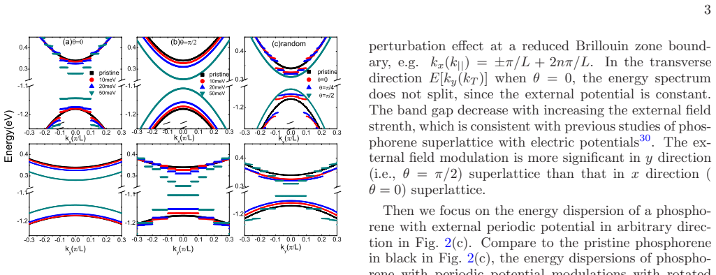
The central claim is that the direction and strength of a periodic potential superlattice are control parameters for phosphorene's electronic and optical anisotropy, not just perturbations. When the superlattice is aligned with the armchair ($x$) direction, band gaps open at the reduced Brillouin-zone boundary and grow with potential strength; when aligned with the zigzag ($y$) direction, the modulation is stronger, flattening the dispersion along $y$ and increasing the effective mass there. Rotating the stripes by an angle $\theta$ mixes the two crystal directions through the rotated band parameters $\alpha'$, $\beta'$, $\lambda$, producing orientation-dependent energy spectra and effective-mass tensors for both electrons and holes. The optical absorption spectrum follows the same tuning: the band edge shifts to lower energy, the absorption strength drops as $\theta$ increases (with a hump near $\theta=0.4\pi$), and the maximum absorption can be varied by more than an order of magnitude. The paper takes this as evidence that rotatable periodic potentials provide an effective band-engineering tool for phosphorene-based optoelectronics.
Load-bearing premise
The result rests on treating the striped gate as a smooth cosine potential $U(x)=V_0\cos(2\pi x/W)$ with $W=10$ nm and $L=20$ nm; if the real potential is more like a square wave, or if the plane-wave expansion is not converged for these parameters, the predicted mini-bands, effective masses, and absorption spectra could change substantially.
Editorial extensions
If this is right
- A single phosphorene layer under striped gates becomes a tunable absorber: varying the stripe angle from 0 to $\pi/2$ moves the band edge to lower photon energies and reduces absorption strength by over an order of magnitude.
- Rotating the superlattice by $90^\circ$ swaps which crystal direction is flattened, so transport anisotropy—the ratio of electron or hole effective masses along $x$ and $y$—can be switched by rotating the gates.
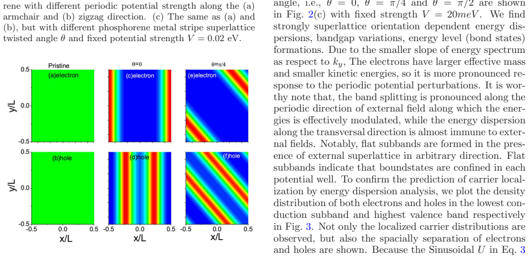
- The superlattice induces spatial separation of electrons and holes by half a period, so optical transitions become spatially indirect in the potential landscape, weakening absorption; this is a built-in knob for emission or detection efficiency.
- The orientation-dependent absorption spectrum itself acts as a probe: the shift of the band edge and the hump near $\theta=0.4\pi$ could be used to verify the stripe angle and the band splitting in an experiment.
Reading between the lines
- The same rotated-stripe calculation could be run with the k·p parameters of other anisotropic 2D semiconductors (for example group-VA monolayers); the mechanism predicts that materials with stronger intrinsic mass anisotropy will show an even larger orientation-tuning range of absorption.
- A real gate produces a potential closer to a square wave than a cosine; checking how the mini-band structure changes when higher Fourier harmonics are added would tell whether the predicted order-of-magnitude absorption tuning survives in actual devices.
- The spatial electron–hole separation under a pure sinusoidal potential suggests a striped-gate device could collect photogenerated carriers at different electrodes; a photocurrent measurement as a function of stripe angle would be a direct, testable consequence of the paper's picture.
Signed reviews
Editorial analysis
A structured set of objections, weighed in public.
Referee Report
Summary. The manuscript investigates the electronic and optical properties of monolayer phosphorene modulated by a one-dimensional periodic electrostatic potential superlattice of arbitrary orientation. Using a two-band k.p effective-mass Hamiltonian with parameters taken from the literature, the authors compute miniband dispersions, carrier density distributions, effective mass tensors, and optical absorption spectra as functions of potential strength and orientation angle. They report orientation-dependent band splitting, flat subbands, spatially separated electron and hole densities, and a substantial reduction of optical absorption with increasing twist angle, which they characterize as tunable by more than an order of magnitude. The central claim is that an artificial potential superlattice can systematically tune the intrinsic electronic and optical anisotropy of phosphorene.
Significance. If the quantitative predictions are correct, the paper provides a useful systematic map of phosphorene-superlattice properties that could inform the design of tunable mid-infrared optoelectronic devices. The strengths of the work include the use of a standard k.p framework with parameters taken from prior literature rather than fitted to the reported spectra, a broad parameter sweep over potential strength and orientation, and concrete, falsifiable predictions for dispersions, effective masses, and absorption. The qualitative picture—flat bands, carrier localization, and orientation-dependent response—is physically plausible. However, the central quantitative claim is currently tied to an ambiguous and internally inconsistent definition of the periodic potential, and the numerical results lack convergence documentation; these issues must be resolved before the order-of-magnitude tunability claim can be accepted.
major comments (3)
- [Section II, after Eq. (4); Fig. 1] The periodic potential is defined as U(x)=V0 cos(2πx/W) with W=10 nm, while L=20 nm is called the superlattice period. A cosine with W=10 nm has spatial period 10 nm, not L=20 nm, yet the Bloch expansion immediately below uses plane waves exp(i(2nπx/L + k_x x)), and the mini-band gaps in Sec. III are described as occurring at kx = ±π/L + 2nπ/L. In addition, Fig. 1 depicts rectangular stripes of width W separated by gaps, which is not a pure cosine profile. Since every subsequent result—dispersions (Fig. 2), carrier densities (Fig. 3), effective masses (Fig. 4), and absorption (Fig. 5)—depends on this potential, the authors must specify unambiguously whether the intended potential is V0 cos(2πx/L), a square wave of period L and stripe width W, or some other profile. If the intended profile is a square wave, the Fourier amplitudes differ: the first harmonic at 2π/L has amplitude 2V0/π for a square wave of peak-to-peak height V0, rather than the full V0 of the cosine, and higher harmonics are present. The reported gaps, effective masses, and absorption spectra would consequently need to be recomputed. This ambiguity is load-bearing for the central claim and must be resolved.
- [Section II, plane-wave expansion; Section III, Figs. 2–5] No convergence information is provided for the plane-wave expansion. The manuscript states that the wave function is expanded in the basis exp(i(2nπx/L + k_x x)) but does not specify the number of reciprocal-lattice vectors retained, nor does it report convergence of band-edge energies, effective masses, or absorption as the truncation is increased. Given the potential strength V0=20 meV relative to the small mini-gaps and the strongly anisotropic k.p dispersion, the truncation could affect quantitative predictions. The authors should report a convergence test—for example, band-edge energies versus the number of basis states—so that the numerical results in Figs. 2–5 can be independently assessed.
- [Abstract and Sec. III, Fig. 5] The abstract claims 'tuning capability more than one order of magnitude in the optical absorption spectrum,' but Fig. 5 plots absorption in arbitrary units and no quantitative definition or normalization of the absorption rate is given. The claim appears to be based on the decrease of the absorption peak with θ in Fig. 5(b), but the vertical scale is unlabeled in absolute terms, and the stated broadening of 0.15 meV affects peak heights. Please specify how α(ℏω) is defined and provide a quantitative comparison (e.g., the peak value at θ=0 versus θ=π/2, or the integrated absorption) that substantiates the order-of-magnitude statement.
minor comments (7)
- [Section II, paragraph after Eq. (4)] The phrase 'the periodic length of the superlattice superlattice' contains a duplicated word, and 'in the new coordination' should read 'in the new coordinate system.'
- [Eq. (5)] The interaction Hamiltonian in Eq. (5) is written as a 4x4 matrix, while the model Hamiltonian in Eqs. (1) and (3) is a 2x2 spinor Hamiltonian; please clarify the basis ordering and the dimensionality of Hint.
- [Table I] The notation in Table I is awkward: 'mcx-mvy are in the unit of electron mass me' and 'α c-β v are in the unit of 10−2 eV·nm2' should be written with explicit subscripts (m_cx, m_cy, m_vx, m_vy and α_c, β_c, α_v, β_v) for readability.
- [Throughout] The potential strength is denoted V in some places (e.g., the Fig. 2 caption) and V0 in Section II; please use a single symbol consistently.
- [Section III, first paragraph] 'bond states' should be 'bound states', and in Section III the text contains 'rotated angel' instead of 'rotated angle'.
- [References] Reference [41] appears to duplicate reference [13]; please remove the duplicate.
- [Section III, optical absorption] The broadening factor of 0.15 meV is introduced without justification; a brief sentence explaining the chosen value would improve reproducibility.
Circularity Check
No significant circularity; the k.p model parameters are external inputs and the superlattice results are computed outputs.
full rationale
The paper's derivation chain starts from a published k.p Hamiltonian for phosphorene (Refs 37-41) with band parameters listed in Table I taken from prior literature; none of these parameters are adjusted to reproduce the reported band structures, effective masses, or absorption spectra. The periodic potential U(x)=V0 cos(2πx/W) with W=10 nm and L=20 nm, the potential strength V0, and the twist angle θ are declared inputs rather than fitted values. The mini-band gaps, flat subbands, effective-mass contours (Fig. 4), and optical absorption spectra (Fig. 5) are numerical outputs of the plane-wave expansion of this model. The 'more than one order of magnitude' absorption change is presented as a consequence of reduced wavefunction overlap, i.e., as a computed result, not as an assumed input. The self-citations (Refs 19, 21, 24, 29) are background on graphene superlattice physics and do not supply a load-bearing theorem or parameter for the present calculation. There is a model-definition concern that the cosine potential with W=10 nm appears inconsistent with the stated superlattice period L=20 nm and with the square-stripe schematic in Fig. 1, but that is a correctness or modeling issue, not circularity: it does not reduce the predictions to their inputs by construction.
Assumptions & free parameters
free parameters (4)
- V0 =
0.02 eV
- W =
10 nm
- L =
20 nm
- broadening =
0.15 meV
assumptions (4)
- domain assumption Two-band k.p Hamiltonian for phosphorene with parameters from Table I
- standard math Bloch theorem and plane wave expansion with a finite basis
- standard math Optical dipole approximation and Fermi golden rule
- ad hoc to paper Cosine form of the periodic potential
Cite this review
Pith. "Pith review of Tunable anisotropic behaviors in phosphorene under periodic potentials in arbitrary directions." pith.science (2026). https://pith.science/paper/5N72P7KL
@misc{pith2026190804199,
  author       = {Pith},
  title        = {Pith review of: Tunable anisotropic behaviors in phosphorene under periodic potentials in arbitrary directions},
  year         = {2026},
  howpublished = {\url{https://pith.science/paper/5N72P7KL}},
  note         = {Machine review of arXiv:1908.04199}
}
read the original abstract
We investigate theoretically the anisotropic electronic and optical behaviors of a monolayer black phosphorus (phosphorene) modulated by periodic potential superlattices in arbitrary directions. We demonstrate that different strength and orientation of the phosphorene potential superlattice can give rise to distinct energy spectra, i.e., tuning the intrinsic electronic anisotropy. Accordingly, the anisotropic effective mass, and optical absorption modulated by superlattice strength and orientation are addressed systematically. This feature enables tuning capability more than one order of magnitude in the optical absorption spectrum. Our findings should be useful in building phosphorene optical and (opto)electronic devices by applying external potential superlattice.
Figures

Figures from the paper (2 more)


Reference graph
Works this paper leans on
-
[1]
Ribeiro-Soares, J., et al., Group theory for structural analysis and lattice vibrations in phosphorene systems. Phys. Rev. B 91, 205421 (2015)
work page 2015
-
[2]
Zhang, S., et al., Recent progress in 2D group-VA semiconductors: from theory to experiment. Chem. Soc. Rev 47, 982 (2018)
work page 2018
-
[3]
Guo, S., et al., 2D V-V Binary Materials: Status and Challenges. Adv. Matter 31, 39, (2019)
work page 2019
-
[4]
Kistanov, A., et al., Large Electronic Anisotropy and Enhanced Chemical Activity of Highly Rippled Phosphorene. J. Phys. Chem. C 120, 6876 (2016)
work page 2016
-
[5]
Kistanov, A., et al., The Role of H2O and O2 Molecules and Phosphorus Vacancies in the Structure Instability of Phosphorene. 2D. Mater. 4(1), 015010 (2017)
work page 2017
-
[6]
Liu, B. and Zhou, K., Recent progress on graphene-analogous 2D nanomaterials: Properties, modeling and applications. Progress in Materials Science 100, 99 (2019)
work page 2019
-
[7]
Nature Communications 5, 4475 (2014)
Qiao, J., et al., High-mobility transport anisotropy and linear dichroism in few-layer black phosphorus. Nature Communications 5, 4475 (2014)
work page 2014
-
[8]
Vy Tran., et al., Layer-Controlled Band Gap and Anisotropic Excitons in Phosphorene. Phys. Rev. B 89, 235319 (2014)
work page 2014
Show all 41 references
-
[9]
Nature Nanotechnology 10, 517 (2015)
Wang, X., et al., Highly anisotropic and robust excitons in monolayer black phosphorus. Nature Nanotechnology 10, 517 (2015)
2015
-
[10]
Nature Communications 5, 4458 (2014)
Xia, F., et al., Rediscovering black phosphorus as an anisotropic layered material for optoelectronics and electronics. Nature Communications 5, 4458 (2014)
2014
-
[11]
Nanotechnology 26, 455202 (2015)
Xie, Y., et al., Photogalvanic effect in monolayer black phosphorus. Nanotechnology 26, 455202 (2015)
2015
-
[12]
Nature Communications 8,1672 (2017)
Chen, X., et al., Widely tunable black phosphorus mid-infrared photodetector. Nature Communications 8,1672 (2017)
2017
-
[13]
Scientific Reports 5, 12295 (2015)
Zhou, X., et al., Landau levels and magnetotransport property of monolayer phosphorene. Scientific Reports 5, 12295 (2015)
2015
-
[14]
Physical Review B 92, 035135 (2015)
Popovic, Z., et al., Electronic structure and anisotropic Rashba spin-orbit coupling in monolayer black phosphorus. Physical Review B 92, 035135 (2015)
2015
-
[15]
H., et al., Anisotropic behaviors of massless Dirac fermions in graphene under periodic potential
Park, C. H., et al., Anisotropic behaviors of massless Dirac fermions in graphene under periodic potential. Nature Physics 4 , 213 (2008)
2008
-
[16]
H., et al., Landau levels and quantum Hall effect in graphene superlattices
Park, C. H., et al., Landau levels and quantum Hall effect in graphene superlattices. Phys. Rev. Lett. 103, 046808 (2009)
2009
-
[17]
and Fertig, H
Brey, L. and Fertig, H. A., Emerging zero modes for graphene in a periodic potential. Phys. Rev. Lett. 103, 046809 (2009)
2009
-
[18]
Barbier, M., et al., Extra Dirac points in the energy spectrum for superlattices on single-layer graphene. Phys. Rev. B 81 , 075438 (2010)
2010
-
[19]
Wu, Z., Electronic fiber in graphene. Appl. Phys. Lett. 98, 082117 (2011)
2011
-
[20]
Maksimova, G. M. et al., Graphene superlattice with periodically modulated Dirac gap. Phys. Rev. B 86, 205422 (2012)
2012
-
[21]
Physics Letters A 376, 1159 (2012)
Wu, Z., et al., Charge pumping in monolayer graphene driven by a series of time-periodic potentials. Physics Letters A 376, 1159 (2012)
2012
-
[22]
and Chan, K
Uddin, S. and Chan, K. S., Band structure of ABC-trilayer graphene superlattice. J. Appl. Phys. 116, 203704 (2014)
2014
-
[23]
Nano Letters 17, 2280 (2017)
Li, Z., et al., Generation of Anisotropic Massless Dirac Fermions and Asymmetric Klein Tunneling in Few-Layer Black Phosphorus Superlattices. Nano Letters 17, 2280 (2017)
2017
-
[24]
Wu, Z., et al., Valley-Dependent Brewster Angles and Goos-Hanchen Effect in Strained Graphene. Phys. Rev. Lett. 106, 176802 (2011)
2011
-
[25]
and De Martino, A., Magnetic superlattice and finite-energy Dirac points in graphene
Dell'Anna, L. and De Martino, A., Magnetic superlattice and finite-energy Dirac points in graphene. Phys. Rev. B 83, 155449 (2011)
2011
-
[26]
Q., et al., Magnetic Kronig-Penney-type graphene superlattices: finite energy Dirac points with anisotropic velocity renormalization
Le, V. Q., et al., Magnetic Kronig-Penney-type graphene superlattices: finite energy Dirac points with anisotropic velocity renormalization. J. Phys.: Condens. Matter. 24, 345502 (2012)
2012
-
[27]
Dell'Anna, L., et al., Using magnetic stripes to stabilize superfluidity in electron-hole double monolayer graphene. Phys. Rev. B 92, 220502(R) (2015)
2015
-
[28]
and Chan, K
Uddin, S. and Chan, K. S., Electric and magnetic superlattices in trilayer graphene. Physica E 75, 56 (2015)
2015
-
[29]
Scientific Reports 7, 6526 (2017)
Li, X., et al., Rashba spin-orbit coupling in graphene monolayer coated by periodic magnetic stripes. Scientific Reports 7, 6526 (2017)
2017
-
[30]
Shota Ono, Effect of one-dimensional superlattice potentials on the band gap of two-dimensional materials. J. Appl. Phys. 121, 204301 (2017)
2017
-
[31]
Zhou, X., et al., Anomalous magneto-optical response of black phosphorus thin films. Phys. Rev. B 92, 165405 (2015)
2015
-
[32]
Zhou, X., et al., Effective g factor in black phosphorus thin films. Phys. Rev. B 95, 045408 (2015)
2015
-
[33]
Nature Nanotechnology 11, 593 (2016)
Li, L., et al., Quantum Hall effect in black phosphorus two-dimensional electron system. Nature Nanotechnology 11, 593 (2016)
2016
-
[34]
Zhang, R., et al., Aharonov-Bohm effect in monolayer phosphorene nanorings. Phys. Rev. B 95, 125418 (2017)
2017
-
[35]
Kang, P., et al., Moir\'e impurities in twisted bilayer black phosphorus: Effects on the carrier mobility, Phys. Rev. B 96, 195406 (2017)
2017
-
[36]
Cao, Y., et al., Correlated insulator behaviour at half-filling in magic-angle graphene superlattices, Nature 556, 80 (2018)
2018
-
[37]
Voon, L., et al., Effective Hamiltonians for phosphorene and silicene. New J. Phys. 17, 025004 (2015)
2015
-
[38]
Fei, R., et al., Topologically protected Dirac cones in compressed bulk black phosphorus. Phys. Rev. B 91, 195319 (2015)
2015
-
[39]
Jiang, Y., et al., Magnetoelectronic properties of multilayer black phosphorus. Phys. Rev. B 92, 085408 (2015)
2015
-
[40]
Faria Junior, P., et al., kp theory for phosphorene: Effective g-factors, Landau levels, and excitons. Phys. Rev. B 100, 115203 (2019)
2019
-
[41]
Scientific Reports 5, 12295 (2015)
Zhou, X., et al., Landau levels and magneto-transport property of monolayer phosphorene. Scientific Reports 5, 12295 (2015)
2015
Reviewed August 14, 2026 · model on record in the stance chip above.
Discussion (0). Continue with ORCID to comment.