Compositional gradient engineering for enhanced ferroelectricity in ultrathin AlScN
Pith reviewed 2026-06-27 08:53 UTC · model grok-4.3
The pith
Compositional grading in AlScN distributes discontinuities to enable ferroelectricity in 5 nm films
A machine-rendered reading of the paper's core claim, the machinery that carries it, and where it could break.
Core claim
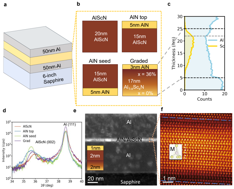
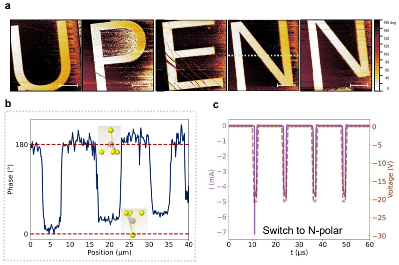
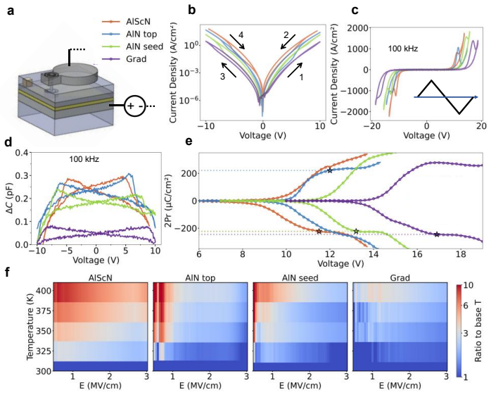
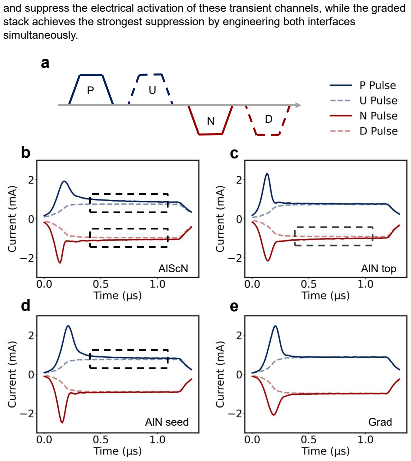
Compositional grading within a continuous wurtzite AlN-AlScN lattice mitigates these limitations by distributing structural and polarization discontinuities across the film thickness, reducing defect formation and local field concentration. In a 20 nm graded heterostructure, monotonic Sc incorporation and AlN-rich boundaries produce reversible ferroelectric switching, an as-grown metal-polar state, a 21% higher breakdown field, 10% enhanced remanent polarization, and 40x higher resistivity relative to homogeneous AlScN. Time-domain PUND measurements reveal strongly suppressed post-switching leakage, consistent with reduced defect-assisted and polarization-coupled conduction. This improved di
What carries the argument
Compositional grading of Sc content in a continuous wurtzite AlN-AlScN lattice that distributes discontinuities across thickness
If this is right
- Graded 20 nm films achieve reversible ferroelectric switching with an as-grown metal-polar state.
- Breakdown field increases by 21% and resistivity by 40 times compared to homogeneous films.
- Remanent polarization is enhanced by 10%.
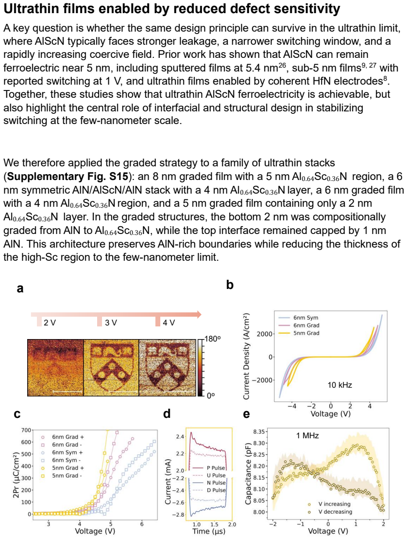
- 5 nm graded stacks show measurable switching near 1 V with only 2 nm active region.
- Post-switching leakage is suppressed due to reduced defect-assisted conduction.
Where Pith is reading between the lines
- The grading approach may transfer to other wurtzite ferroelectrics to improve their thickness scaling.
- Low-voltage operation in ultrathin layers could support higher-density memory arrays without extra interface layers.
- The as-grown metal-polar orientation might simplify device fabrication by removing separate poling steps.
Load-bearing premise
The measured improvements in switching, breakdown, polarization, and resistivity are caused by the compositional grading distributing discontinuities and reducing defects rather than by differences in growth conditions or sample variation.
What would settle it
Growing homogeneous AlScN control films in the same deposition run as the graded samples and checking whether the 21% breakdown improvement, 40x resistivity gain, and 5 nm switching persist.
Figures
read the original abstract
Ferroelectric AlScN is promising for CMOS-compatible non-volatile memory, but thickness scaling is limited by leakage, premature breakdown, and defect-mediated failure. Here we show that compositional grading within a continuous wurtzite AlN-AlScN lattice mitigates these limitations by distributing structural and polarization discontinuities across the film thickness, reducing defect formation and local field concentration. In a 20 nm graded heterostructure, monotonic Sc incorporation and AlN-rich boundaries produce reversible ferroelectric switching, an as-grown metal-polar state, a 21% higher breakdown field, 10% enhanced remanent polarization, and 40x higher resistivity relative to homogeneous AlScN. Time-domain PUND measurements reveal strongly suppressed post-switching leakage, consistent with reduced defect-assisted and polarization-coupled conduction. This improved dielectric robustness enables ferroelectric functionality in 5 nm graded stacks containing only a 2 nm $\mathrm{Al}_{0.64}\mathrm{Sc}_{0.36}\mathrm{N}$ region, with measurable switching near 1 V. These results establish compositional grading as a defect- and field-management strategy for scalable ultrathin wurtzite ferroelectrics.
Editorial analysis
A structured set of objections, weighed in public.
Referee Report
Summary. The manuscript claims that compositional grading within a continuous wurtzite AlN-AlScN lattice mitigates leakage, premature breakdown, and defect-mediated failure in ultrathin ferroelectric AlScN by distributing structural and polarization discontinuities. In 20 nm graded films with monotonic Sc incorporation and AlN-rich boundaries, this yields reversible ferroelectric switching, an as-grown metal-polar state, a 21% higher breakdown field, 10% enhanced remanent polarization, and 40x higher resistivity relative to homogeneous AlScN; time-domain PUND data show suppressed post-switching leakage. The approach also enables measurable switching near 1 V in 5 nm graded stacks containing only a 2 nm Al0.64Sc0.36N region.
Significance. If the performance gains are causally attributable to the spatial Sc profile rather than growth-condition differences, the work would provide a practical defect- and field-management strategy for scaling wurtzite ferroelectrics below 10 nm, directly relevant to CMOS-compatible non-volatile memory. The experimental demonstration of functional 5 nm stacks is potentially impactful, though verification of the mechanism requires matched controls.
major comments (2)
- [Abstract] Abstract (results summary): the reported 21% higher breakdown field, 10% enhanced Pr, and 40x resistivity are compared to 'homogeneous AlScN,' yet no statement confirms that the homogeneous controls were grown with identical time-integrated Sc flux, substrate temperature history, or total growth duration. If the graded films used a ramped flux while homogeneous films used constant flux, the observed improvements could arise from global deposition differences rather than the Sc(z) profile; this is load-bearing for the central claim that grading distributes discontinuities and reduces defects.
- [Abstract] Abstract (methods description): full experimental details on growth, electrode deposition, and measurement protocols (including error bars, number of devices, and exclusion criteria) are absent, preventing assessment of whether the PUND leakage suppression and 1 V switching in 5 nm stacks are reproducible and isolated from sample-to-sample variation.
minor comments (1)
- [Abstract] The abstract uses 'monotonic Sc incorporation' without specifying the exact Sc concentration profile or how it was measured (e.g., via SIMS or EDX); adding this would clarify the grading implementation.
Simulated Author's Rebuttal
We thank the referee for the constructive comments and the opportunity to clarify the experimental controls and methods presentation in our manuscript. We respond to each major comment below.
read point-by-point responses
-
Referee: [Abstract] Abstract (results summary): the reported 21% higher breakdown field, 10% enhanced Pr, and 40x resistivity are compared to 'homogeneous AlScN,' yet no statement confirms that the homogeneous controls were grown with identical time-integrated Sc flux, substrate temperature history, or total growth duration. If the graded films used a ramped flux while homogeneous films used constant flux, the observed improvements could arise from global deposition differences rather than the Sc(z) profile; this is load-bearing for the central claim that grading distributes discontinuities and reduces defects.
Authors: We agree that explicit confirmation of matched growth conditions is essential to support the central claim. The homogeneous AlScN films were grown using constant Sc flux calibrated to the time-integrated Sc incorporation of the graded films, with identical substrate temperature history and total growth duration, as detailed in the Methods section. To address the referee's concern directly in the abstract, we will revise it to include a concise statement confirming these matched parameters for the controls. revision: yes
-
Referee: [Abstract] Abstract (methods description): full experimental details on growth, electrode deposition, and measurement protocols (including error bars, number of devices, and exclusion criteria) are absent, preventing assessment of whether the PUND leakage suppression and 1 V switching in 5 nm stacks are reproducible and isolated from sample-to-sample variation.
Authors: We acknowledge that the abstract omits these specifics due to length constraints. The full manuscript includes a Methods section with growth, electrode, and PUND protocols. We will revise the abstract to reference the number of devices, typical error bars, and note that full details (including exclusion criteria) are provided in Methods to facilitate assessment of reproducibility. revision: yes
Circularity Check
No circularity: purely experimental claims with no derivations or models
full rationale
The paper reports experimental fabrication and electrical characterization of compositionally graded AlScN films versus homogeneous controls. All central claims (reversible switching, higher breakdown field, enhanced polarization, higher resistivity, and functionality at 5 nm) rest on direct measurements (PUND, I-V, etc.) rather than any derivation, equation, fitted parameter, or self-citation chain. No mathematical model, uniqueness theorem, ansatz, or prediction step exists that could reduce to its own inputs. The comparison to homogeneous samples is presented as an empirical control; any debate about whether the controls are perfectly matched belongs to experimental validity, not circularity of a derivation. The work is therefore self-contained against external benchmarks with score 0.
Axiom & Free-Parameter Ledger
Reference graph
Works this paper leans on
-
[1]
Wave-number-dependent dielectric function of semiconductors
Penn DR. Wave-number-dependent dielectric function of semiconductors. Physical review 1962, 128(5): 2093
1962
-
[2]
Two-dimensional devices and integration towards the silicon lines
Wang S, Liu X, Xu M, Liu L, Yang D, Zhou P. Two-dimensional devices and integration towards the silicon lines. Nature materials 2022, 21(11): 1225-1239
2022
-
[3]
Single-crystalline van der Waals layered dielectric with high dielectric constant
Zhang C, Tu T, Wang J, Zhu Y, Tan C, Chen L, et al. Single-crystalline van der Waals layered dielectric with high dielectric constant. Nature materials 2023, 22(7): 832-837
2023
-
[4]
Semiconductors used in photovoltaic and photocatalytic devices: assessing fundamental properties from DFT
Le Bahers T, Rerat M, Sautet P. Semiconductors used in photovoltaic and photocatalytic devices: assessing fundamental properties from DFT. The Journal of Physical Chemistry C 2014, 118(12): 5997-6008
2014
-
[5]
Molybdenum disulfide transistors with enlarged van der Waals gaps at their dielectric interface via oxygen accumulation
Luo P, Liu C, Lin J, Duan X, Zhang W, Ma C, et al. Molybdenum disulfide transistors with enlarged van der Waals gaps at their dielectric interface via oxygen accumulation. Nature Electronics 2022, 5(12): 849-858
2022
-
[6]
High-K materials and metal gates for CMOS applications
Robertson J, Wallace RM. High-K materials and metal gates for CMOS applications. Materials Science and Engineering: R: Reports 2015, 88: 1-41
2015
-
[7]
High-κ perovskite membranes as insulators for two-dimensional transistors
Huang J-K, Wan Y, Shi J, Zhang J, Wang Z, Wang W, et al. High-κ perovskite membranes as insulators for two-dimensional transistors. Nature 2022, 605(7909): 262-267
2022
-
[8]
High-κ monocrystalline dielectrics for low-power two-dimensional electronics
Yin L, Cheng R, Wan X, Ding J, Jia J, Wen Y, et al. High-κ monocrystalline dielectrics for low-power two-dimensional electronics. Nature Materials 2025, 24(2): 197-204
2025
-
[9]
Crystal structure and band gap determination of HfO2 thin films
Cheynet MC, Pokrant S, Tichelaar FD, Rouvière J-L. Crystal structure and band gap determination of HfO2 thin films. Journal of Applied Physics 2007, 101(5)
2007
-
[10]
Electronic band structure of zirconia and hafnia polymorphs from the W perspective
Jiang H, omez-Abal RI, Rinke P, Scheffler M. Electronic band structure of zirconia and hafnia polymorphs from the W perspective. Physical Review B— Condensed Matter and Materials Physics 2010, 81(8): 085119
2010
-
[11]
Demonstration and STEM analysis of ferroelectric switching in MOCVD‐grown single crystalline Al0
Wolff N, Schönweger , Streicher I, Islam MR, Braun N, Straňák P, et al. Demonstration and STEM analysis of ferroelectric switching in MOCVD‐grown single crystalline Al0. 85Sc0. 15N. Advanced Physics Research 2024, 3(5): 2300113
2024
-
[12]
Experimental determination of giant polarization in wurtzite III-nitride semiconductors
Ye H, Wang P, Wang R, Wang J, Xu X, Feng R, et al. Experimental determination of giant polarization in wurtzite III-nitride semiconductors. Nature Communications 2025, 16(1): 3863
2025
-
[13]
Ferroelectric N-polar ScAlN/ aN heterostructures grown by molecular beam epitaxy
Wang P, Wang D, Mondal S, Mi Z. Ferroelectric N-polar ScAlN/ aN heterostructures grown by molecular beam epitaxy. Applied Physics Letters 2022, 121(2)
2022
-
[14]
Polarity inversion of ferroelectric AlScN films by radio frequency power
Zhao Y, Kang Y, Wu X, Zhang B, Zhou D, Tong Y, et al. Polarity inversion of ferroelectric AlScN films by radio frequency power. Thin Solid Films 2025: 140830
2025
-
[15]
Effect of Sc content on the polarity of AlScN thin films deposited on indium tin oxide by radio frequency-magnetron sputtering
Liu X, Abe K, Yuan X, Okamoto K, Funakubo H, Kondo S, et al. Effect of Sc content on the polarity of AlScN thin films deposited on indium tin oxide by radio frequency-magnetron sputtering. Japanese Journal of Applied Physics 2025, 64(8): 08SP17
2025
-
[16]
Anomalously abrupt switching of wurtzite -structured ferroelectrics: simultaneous non-linear nucleation and growth model
Yazawa K, Hayden J, Maria J-P, Zhu W, Trolier-McKinstry S, Zakutayev A, et al. Anomalously abrupt switching of wurtzite -structured ferroelectrics: simultaneous non-linear nucleation and growth model. Materials Horizons 2023, 10(8): 2936-2944
2023
-
[17]
Influence of Ion Energy on the Surface Polarity of AlScN Thin Films During Sputter Process
Yun S, o D, Lee P-C, Kummel A. Influence of Ion Energy on the Surface Polarity of AlScN Thin Films During Sputter Process. 2025 IEEE International Interconnect Technology Conference (IITC); 2025: IEEE; 2025. p. 1-3
2025
-
[18]
Van der Waals engineering of ferroelectric heterostructures for long-retention memory
Wang X, Zhu C, Deng Y, Duan R, Chen J, Zeng Q, et al. Van der Waals engineering of ferroelectric heterostructures for long-retention memory. Nature communications 2021, 12(1): 1109
2021
-
[19]
Ferroelectric Zr0
Müller J, Böscke T, Bräuhaus D, Schröder U, Böttger U, Sundqvist J, et al. Ferroelectric Zr0. 5Hf0. 5O2 thin films for nonvolatile memory applications. Applied Physics Letters 2011, 99(11)
2011
-
[20]
A rhombohedral ferroelectric phase in epitaxially strained Hf0
Wei Y, Nukala P, Salverda M, Matzen S, Zhao HJ, Momand J, et al. A rhombohedral ferroelectric phase in epitaxially strained Hf0. 5Zr0. 5O2 thin films. Nature materials 2018, 17(12): 1095-1100
2018
-
[21]
Enhanced ferroelectricity in ultrathin films grown directly on silicon
Cheema SS, Kwon D, Shanker N, Dos Reis R, Hsu S-L, Xiao J, et al. Enhanced ferroelectricity in ultrathin films grown directly on silicon. Nature 2020, 580(7804): 478-482
2020
-
[22]
Scaling of structure and electrical properties in ultrathin epitaxial ferroelectric heterostructures
Nagarajan V, Junquera J, He J, Jia C, Waser R, Lee K, et al. Scaling of structure and electrical properties in ultrathin epitaxial ferroelectric heterostructures. Journal of applied physics 2006, 100(5)
2006
-
[23]
Critical thickness of ultrathin ferroelectric BaTiO3 films
Kim Y, Kim D, Kim J, Chang Y, Noh T, Kong J, et al. Critical thickness of ultrathin ferroelectric BaTiO3 films. Applied Physics Letters 2005, 86(10)
2005
-
[24]
Ultrathin oriented BiFeO3 films from deposition of atomic layers with greatly improved leakage and ferroelectric properties
Liu Y-T, Ku C-S, Chiu S-J, Lee H-Y, Chen S-Y. Ultrathin oriented BiFeO3 films from deposition of atomic layers with greatly improved leakage and ferroelectric properties. ACS Applied Materials & Interfaces 2014, 6(1): 443-449
2014
-
[25]
Ferroelectricity in atomic-scale titanium dioxide dielectric films
Das K, Reidy K, Husain S, Park JH, Jayakumar H, Thampy V, et al. Ferroelectricity in atomic-scale titanium dioxide dielectric films. Science 2026: eaec9417
2026
-
[26]
Room temperature in- plane ferroelectricity in van der Waals In2Se3
Zheng C, Yu L, Zhu L, Collins JL, Kim D, Lou Y, et al. Room temperature in- plane ferroelectricity in van der Waals In2Se3. Science advances 2018, 4(7): eaar7720
2018
-
[27]
Effects of scaling the film thickness on the ferroelectric properties of SrBi 2 Ta 2 O 9 ultra thin films
Celinska J, Joshi V, Narayan S, McMillan L, Paz de Araujo C. Effects of scaling the film thickness on the ferroelectric properties of SrBi 2 Ta 2 O 9 ultra thin films. Applied physics letters 2003, 82(22): 3937-3939
2003
-
[28]
Fabrication of Ultrathin Ferroelectric Al0
Ryoo SK, Kim KD, Choi W, Sriboriboon P, Heo S, Seo H, et al. Fabrication of Ultrathin Ferroelectric Al0. 7Sc0. 3N Films under Complementary‐Metal‐Oxide‐ Semiconductor Compatible Conditions by using HfN0. 4 Electrode. Advanced Materials 2025, 37(1): 2413295
2025
-
[29]
In‐ grain ferroelectric switching in sub‐5 nm thin Al0
Schönweger , Wolff N, Islam MR, remmel M, Petraru A, Kienle L, et al. In‐ grain ferroelectric switching in sub‐5 nm thin Al0. 74Sc0. 26N films at 1 V. Advanced Science 2023, 10(25): 2302296
2023
-
[30]
Optical processes in semiconductors
Pankove JI. Optical processes in semiconductors. Courier Corporation, 2012
2012
-
[31]
Optical constants and band gap of wurtzite Al1− xScxN/Al2O3 prepared by magnetron sputter epitaxy for scandium concentrations up to x= 0.41
Baeumler M, Lu Y, Kurz N, Kirste L, Prescher M, Christoph T, et al. Optical constants and band gap of wurtzite Al1− xScxN/Al2O3 prepared by magnetron sputter epitaxy for scandium concentrations up to x= 0.41. Journal of Applied Physics 2019, 126(4)
2019
discussion (0)
Sign in with ORCID, Apple, or X to comment. Anyone can read and Pith papers without signing in.