REVIEW 1 major objections 6 minor 1 references
Understanding the image contrast of material boundaries in IR nanoscopy reaching 5 nm spatial resolution
T0 review · 1 major / 6 minor · reviewed 2026-08-14 · deepseek-v4-flash
Pith's one-line read This paper shows that s-SNOM line profiles across metal–dielectric boundaries are intrinsically asymmetric because the metal screens the tip's near field, and that ultra-sharp tungsten tips reduce the apparent boundary width to about 5 nm.
desk verdict Solid experimental paper: first clean evidence that s-SNOM edge responses are asymmetric, with a sensible (if not fully nailed) screening explanation; the '5 nm resolution' title needs qualification. read the letter →
The pith
A machine-rendered reading of the paper's core claim, the machinery that carries it, and where it could break.
The reading
What carries the argument
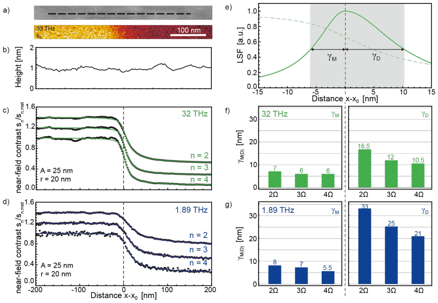
The carrying object is the asymmetric edge response function: the measured near-field amplitude across the boundary is fit to an integral of a piecewise Lorentzian, giving a line spread function with two different half-widths, $\gamma_M$ on the metal side and $\gamma_D$ on the dielectric side, and a total apparent width $w=\gamma_M+\gamma_D$. The explanatory mechanism is sample-dependent confinement and screening of the near field at the tip apex: a metal surface screens the tip's near field so strongly that the tip only senses the boundary when within about 5 nm of it, whereas the dielectric permits near-field interaction across the boundary from tens of nanometres away. The numerical simulation computes the tip-scattered field from a surface-charge integral over an idealized conical tip and reproduces both the asymmetry and the Lorentzian shape of the near-field profile.
What would settle it
Measure s4 line profiles at an uncovered, atomically sharp metal–dielectric edge with no capping layer using tips of several known radii (for example 3, 10, and 25 nm); the screening explanation predicts that the metal-side half-width $\gamma_M$ stays at a few nanometres and does not scale with tip radius, whereas growth of $\gamma_M$ in proportion to tip diameter would contradict the claimed order-of-magnitude metal-side screening.
Extended reading notes
Core claim
On its own terms, the paper establishes that the edge response of an s-SNOM across a sharp metal–dielectric boundary is an asymmetric function, described by a piecewise Lorentzian line spread function whose half-width on the metal side is three to four times smaller than on the dielectric side. The metal-side probing range can be an order of magnitude below the tip apex diameter; the authors explain this by screening of the tip's near field by the metal sample, which prevents the tip from sensing the boundary until it is within a few nanometres of the interface. The same asymmetric screening appears in full-wave simulations with a conical metal tip over a perfect boundary, and the simulated line profile matches the measured one after normalization. The paper additionally shows that focused-ion-beam sharpened tungsten tips with apex radius near 3 nm, operated at 12 nm tapping amplitude, reduce the apparent edge width to about 5 nm, with the remaining limitation on the metal side attributed to the atomic-scale dielectric capping layer that makes the true boundary a subsurface object.
Load-bearing premise
The load-bearing premise is that the idealized full-wave simulation—a perfectly sharp conical tip, a perfect metal–dielectric step, and literature permittivities—captures the same near-field physics as the real experiment, where the tip is pyramidal, the edge is slightly rounded, and a 1.5 nm capping layer covers the metal; if that model misrepresents the metal-side confinement, the screening explanation loses its support.
Editorial extensions
If this is right
- Boundary positions extracted from s-SNOM line profiles do not sit at the center of the signal transition, so locating the true material interface requires an asymmetric two-sided fit.
- A one-sided tail in a near-field line profile is not by itself evidence of a gradual material change, diffusion, or doping gradient, because a perfectly sharp boundary produces the same signature.
- Spatial resolution at a metal–dielectric edge is not set by tip radius alone: a standard ~50 nm tip yields an apparent width around 20 nm, while an r = 3 nm tungsten tip at 12 nm tapping amplitude reaches about 5 nm.
- The same screening effect is expected at boundaries between high- and low-index dielectrics, so asymmetric edge analysis should apply beyond metal samples.
Reading between the lines
- A testable extension would be to scan a boundary between two dielectrics of high and low refractive index with no topography; if the screening picture holds, the asymmetry should grow with permittivity contrast rather than with conductivity.
- The two-sided line spread function means a single-number resolution figure for s-SNOM is ambiguous unless the side of the boundary is specified.
- Removing or thinning the dielectric capping layer on the metal side should improve the metal-side half-width further, potentially pushing the apparent edge below the demonstrated 5 nm.
- The same screening argument suggests that depositing target molecules on a metal near a sharp edge could localize the near-field interaction and yield sub-5 nm chemical contrast without sharper tips.
Signed reviews
Editorial analysis
A structured set of objections, weighed in public.
Referee Report
Summary. This paper investigates the image contrast of scattering-type scanning near-field optical microscopy (s-SNOM) across a sharp metal–dielectric boundary using a commercial hard disk drive read/write head as a topography-free test sample. The authors report that line profiles across the boundary are not point-symmetric for both IR (9.3 µm) and THz (158 µm) illumination, with the asymmetry quantified by fitting the profiles to a piecewise arctangent function whose derivative is a piecewise Lorentzian with different half-widths on the metal and dielectric sides. They attribute the asymmetry to sample-dependent screening of the tip's near field by the metal, which shortens the probing range on the metal side. Full-wave simulations with an idealized conical tip and a perfect material boundary reproduce the asymmetry, though they over-predict its magnitude, which the authors attribute to the rounded experimental boundary and pyramidal tip. The paper further demonstrates that with focused-ion-beam-sharpened tungsten tips of ~3 nm radius and reduced tapping amplitude, the apparent boundary width can be reduced to about 5 nm.
Significance. If the claims hold, the paper provides important new insights into s-SNOM image formation: it shows for the first time that asymmetric edge-response functions can be intrinsic to the near-field interaction at a sharp material boundary, rather than being caused by sample gradients or topography. The introduction of the HDD read/write head as a topography-free resolution standard is a valuable methodological contribution, and the direct demonstration of sub-10 nm apparent boundary width with sharp tips is of practical interest. The experimental procedure is thorough: line profiles are averaged (20–50 profiles), cross-correlated for alignment, and fit with an asymmetric function that is shown to be superior to a symmetric fit. The simulations use literature permittivities, so the comparison is not circular. The main weakness is that the screening mechanism is supported by a single idealized simulation, which leaves some room for alternative explanations.
major comments (1)
- [Figure 4 – Numerical simulation] The screening explanation of the line-profile asymmetry is supported primarily by the full-wave simulation shown in Fig. 4, which models the sample as a perfectly sharp metal–dielectric boundary and the tip as an idealized 8 µm conical tip with r = 25 nm. As the authors note in the text, the simulation over-predicts the asymmetry, essentially on the dielectric side, which they attribute to the rounded boundary and pyramidal tip shape in the experiment. However, because a perfectly sharp metallic edge can produce a strong local field singularity that skews the computed line profile in the same direction as the proposed screening effect, the simulated asymmetry in Fig. 4b may be partly an artifact of this idealization. To establish that the asymmetry is indeed a consequence of metal-side screening rather than of the edge singularity, I recommend performing a control simulation with a rounded boundary (e.g., a finite radius of curvature of a few nanometers) or, alternatively, comparing the simulated line profile with a calculation of the near-field confinement on homogeneous metal and dielectric substrates. This would provide a quantitative test of the screening mechanism and would strengthen the central claim of the paper.
minor comments (6)
- [Abstract] The phrase 'well20 defined' in the abstract appears to be a formatting artifact and should be corrected to 'well-defined'.
- [Introduction and Fig. 2f,g] The width w is defined as γM + γD, the sum of the half-widths of the asymmetric line-spread function; because the line-spread function is not centered on the boundary, the authors should explicitly state this operational definition and discuss how it relates to conventional resolution criteria such as Rayleigh or Sparrow.
- [Numerical simulation (Fig. 4)] The sentence stating that 'no lateral shift in x-direction was applied to the simulated data (Fig. 2c)' should refer to Fig. 4b, not Fig. 2c.
- [Methods] The word 'grove' in the description of the FIB tip fabrication should be 'groove'.
- [Fig. 2 caption] The caption describes the fit lines as 'green/blue lines', while the text refers to 'green and blue solid curves'; the colors and labeling should be made consistent.
- [Fig. 2 and Methods] The fitted parameters γM and γD are reported without uncertainties; providing standard errors or confidence intervals, and ideally a statistical comparison (e.g., chi-squared) between the asymmetric and symmetric fits, would strengthen the claim that the asymmetry is statistically significant.
Circularity Check
No significant circularity: the central claims rest on direct measurements and independent full-wave simulations, not on fitted or self-cited inputs.
full rationale
The paper's central claims are (i) that s-SNOM line profiles across a sharp metal-dielectric boundary are non-point-symmetric, (ii) that this asymmetry is caused by sample-dependent screening that shortens the near-field probing range on the metal side, and (iii) that ultra-sharp W tips reduce the apparent boundary width to about 5 nm. Claim (i) is supported directly by averaged experimental line profiles; the piecewise-arctan fit with different HWHMs on the metal and dielectric sides is a descriptive summary of the data, and the authors explicitly show that a symmetric fit agrees much worse (Supporting Information S2, S3). Thus the asymmetry is not manufactured by the fit function but is a measured property of the data. Claim (ii) is supported by a Comsol full-wave simulation using literature permittivities (epsilon_M=-1200+750i, epsilon_D=1.05+0.19i, ref 36) and a conical tip geometry; the simulated line profile is obtained by computing the tip dipole moment and harmonic demodulation, not by imposing an asymmetric line shape. The screening explanation is an interpretation of the computed near-field distributions in Fig. 4c,d, not an input to the calculation. The acknowledged mismatch, where the idealized sharp boundary and conical tip over-predict the asymmetry, is an honest modeling limitation rather than circularity. Claim (iii) is a direct measurement with FIB-sharpened W tips and does not depend on the simulation. Self-citations in the paper concern tip fabrication, THz antenna tips, and subsurface-resolution methods (refs 25, 28, 29, 32, 35); none is load-bearing for the new screening mechanism, and no uniqueness theorem is invoked to exclude alternatives. The line-profile fit is empirically motivated, and the connection between the simulated Lorentzian near-field profile and the fit form is explicitly hedged ('further studies are required'). No derivational step reduces to its own inputs by construction, so the paper is not circular.
Assumptions & free parameters
free parameters (1)
- Piecewise arctan fit parameters (f_M, f_D, γ_M, γ_D, x0, b) =
Values per line profile; e.g., for Pt/Ir tip at A=25 nm IR s4: γ_M ≈ 4-5 nm, γ_D ≈ 12-20 nm, w = γM+γD ≈ 16.5-23.5 nm…
assumptions (5)
- standard math The tip-scattered field Esca is proportional to the induced dipole moment P = ∫ σ(r) r dr over the tip surface (Eq. 1).
- domain assumption Demodulating the tip-scattered signal at the n-th harmonic of the tip oscillation yields a background-free near-field signal equal to the n-th Fourier coefficient of the time-dependent scattered field.
- domain assumption The derivative of the edge response function is the line spread function, and its width (γM + γD) is a valid measure of spatial resolution.
- domain assumption The sample permittivities at 32 THz are εM = -1200 + 750i (metal) and εD = 1.05 + 0.19i (Al2O3), taken from the literature.
- domain assumption The simplified simulation geometry (conical tip, perfect boundary) is sufficiently faithful to reveal the near-field screening mechanism.
Cite this review
Pith. "Pith review of Understanding the image contrast of material boundaries in IR nanoscopy reaching 5 nm spatial resolution." pith.science (2026). https://pith.science/paper/A6R7STHL
@misc{pith2026190805068,
  author       = {Pith},
  title        = {Pith review of: Understanding the image contrast of material boundaries in IR nanoscopy reaching 5 nm spatial resolution},
  year         = {2026},
  howpublished = {\url{https://pith.science/paper/A6R7STHL}},
  note         = {Machine review of arXiv:1908.05068}
}
read the original abstract
Scattering-type scanning near-field optical microscopy (s-SNOM) allows for nanoscale resolved Infrared (IR) and Terahertz (THz) imaging, and thus has manifold applications ranging from materials to biosciences. However, a quantitatively accurate understanding of image contrast formation at materials boundaries, and thus spatial resolution is a surprisingly unexplored terrain. Here we introduce the write/read head of a commercial hard disk drive (HDD) as a most suitable test sample for fundamental studies, given its well20 defined sharp material boundaries perpendicular to its ultra-smooth surface. We obtainunprecedented and unexpected insights into the s-SNOM image formation process, free of topography-induced artifacts that often mask and artificially modify the pure near-field optical contrast. Across metal-dielectric boundaries, we observe non-point-symmetric line profiles for both IR and THz illumination, which are fully corroborated by numericalsimulations. We explain our findings by a sample-dependent confinement and screening of the near fields at the tip apex, which will be of crucial importance for an accurate understanding and proper interpretation of high-resolution s-SNOM images of nanocomposite materials. We also demonstrate that with ultra-sharp tungsten tips the apparent width (and thus resolution) of sharp material boundaries can be reduced to about 5 nm.
Figures

Reference graph
Works this paper leans on
-
[1]
This document is the Accepted Manuscript version of a Published Work that appeared in final form in ACS Photonics copyright © American Chemical Society after peer review and technical editing by the publisher. Understanding the image contrast of material boundaries in IR nanoscopy reaching 5 nm spatial resolution Stefan Mastel1, Alexander A. Govyadinov1, ...
work page 2016
Reviewed August 14, 2026 · model on record in the stance chip above.
Discussion (0). Continue with ORCID to comment.