REVIEW 2 major objections 6 minor 96 references
The importance of second order deformation potentials in modeling of InAs/GaAs nanostructures
T0 review · 2 major / 6 minor · reviewed 2026-08-14 · deepseek-v4-flash
Pith's one-line read Adding quadratic strain terms lets 8-band k.p reproduce atomistic tight-binding results for InAs/GaAs nanostructures
desk verdict A careful, honest calibration of second-order strain terms for 8-band k.p against tight-binding; the electron-state improvement is large and usable, though external validity remains tied to the Jancu TB reference. read the letter →
The pith
A machine-rendered reading of the paper's core claim, the machinery that carries it, and where it could break.
The reading
What carries the argument
The load-bearing object is the second-order strain Hamiltonian appended to the 8-band k.p model, introducing six deformation potentials fitted to sp3d5s* tight-binding bulk band edges under hydrostatic, uniaxial, and biaxial strain. It corrects the curvature of the conduction and valence band edges as a function of strain, which the linear Bir-Pikus theory gets wrong at large lattice mismatch. The paper also derives a single effective parameter for a biaxial-strain term in one-band effective-mass calculations. Quadratic shear-strain terms are omitted because of uncertainty in the internal sublattice displacement parameter and because the reference tight-binding model has limited accuracy for shear strains.
What would settle it
Compute the InAs and GaAs bulk band-edge shifts under biaxial strain with an independent method not used in the fitting, for example density-functional theory or a direct experimental determination of hydrostatic and biaxial deformation potentials. If the resulting curvatures disagree with the fitted second-order deformation potentials by more than the quoted few-meV target, the nanostructure agreement reported here is largely a consequence of fitting to the same reference model rather than a physically independent validation.
Extended reading notes
Core claim
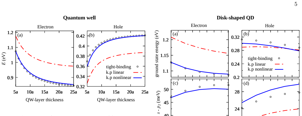
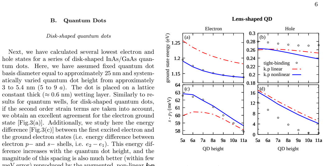
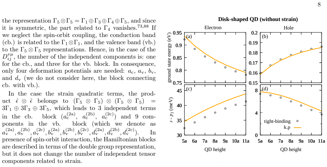
The paper's central claim is that 8-band k.p with quadratic strain terms reproduces the sp3d5s* tight-binding single-particle spectrum for InAs/GaAs structures across geometries. For quantum wells of 3 to 15 nm thickness, the electron ground state agrees to at most about 10 meV; for disk-shaped dots the e1-h1 gap error drops from about 100 meV with linear k.p to about 15 meV with the nonlinear scheme, and electron s-p shell spacings match within a few meV. The improvement is traced to the strongly nonlinear response of band edges to biaxial strain at the roughly 7 percent lattice mismatch. The authors are careful that the agreement is best for electron states and flat geometries; hole states in lens-shaped dots remain off by 20 to 30 meV, which they attribute to shear-strain sensitivity and to limitations of the tight-binding reference for shear strain.
Load-bearing premise
The whole calculation assumes that the atomistic tight-binding model is the correct ground truth for how the material's electronic levels shift under strain, and the paper itself notes that this reference is least reliable for exactly the shear strains that cause the largest remaining discrepancies.
Editorial extensions
If this is right
- For InAs/GaAs quantum wells and flat disk-shaped quantum dots, nonlinear 8-band k.p can replace sp3d5s* tight-binding for electron ground-state energies and s-p shell spacings, at a fraction of the computational cost.
- The single-particle gap in disk-shaped dots is predicted with a residual error of about 15 meV instead of about 100 meV, making computed excitonic and optical transition energies in this material system more reliable for device modeling.
- The published parameter sets for InAs and GaAs allow other groups to include second-order strain effects without refitting.
- Hole states and curved lens-shaped dots remain the known weak spot, with 20 to 30 meV errors that the paper ties to shear strain; improving shear-related deformation potentials is the next step.
- The effective-mass parameterization provides a quick way to incorporate strain nonlinearity into large-scale or few-band device simulations.
- Going beyond the paper: the same fitting pipeline could be transferred to other lattice-mismatched III-V systems, since the linear Bir-Pikus failure under biaxial strain is a general feature and the paper's parameter sets cover only InAs and GaAs.
- Going beyond the paper: the residual hole-state errors being concentrated in shear strain suggests a testable shape dependence, namely that lens-shaped dots, with stronger shear, should show larger k.p-versus-tight-binding gap discrepancies than disk-shaped dots of comparable size.
- Going beyond the paper: if the fitted second-order potentials are physically correct, they should also modify strained-dot quantities the paper does not report, such as spin-orbit splittings and effective g-factors, so measuring those would provide an independent check.
Signed reviews
Editorial analysis
A structured set of objections, weighed in public.
Referee Report
Summary. This manuscript extends the 8-band k.p Hamiltonian for InAs/GaAs by adding terms quadratic in strain (second-order deformation potentials), with parameters fitted to bulk band edges from the Jancu sp3d5s* empirical tight-binding model. It then compares linear and nonlinear k.p results for electron and hole states in InAs/GaAs quantum wells and in disk- and lens-shaped quantum dots against the same TB model. The authors find that linear k.p overestimates electron confinement energies by about 100 meV in quantum wells and disk-shaped dots, while the nonlinear model reduces the discrepancy to roughly 10 meV for quantum-well electrons and to about 15 meV for the single-particle gap in disk-shaped dots; hole states in lens-shaped dots remain 20-30 meV off. Parameter tables and an effective-mass parameterization are provided.
Significance. The paper's contribution is a parameterized, computationally cheap k.p scheme that reproduces a widely used atomistic TB model for electron states in biaxial-strain-dominated InAs/GaAs nanostructures, together with an honest assessment of where it fails (holes, shear strain, curved dots). The out-of-sample transfer from bulk homogeneous strain fitting to inhomogeneously strained confined states is nontrivial and gives the comparison real content. The full parameter sets and the explicit discussion of omitted second-order shear terms are valuable for practitioners. The main limitation is that the reference model is also the fitting target, so the physical accuracy of the second-order potentials for real materials is not independently established.
major comments (2)
- [Sec. II (Table I) and Sec. III (Figs. 2-4)] All six second-order deformation potentials in Table I are fitted to the Jancu sp3d5s* TB model (Ref. 79), and the nanostructure benchmark in Figs. 2-4 uses that same model. The nanostructure comparison is therefore a consistency check of transferability from homogeneous bulk strain to confined nanostructures, not an independent validation of the potentials. Since the authors themselves note in Sec. II that the Jancu parameterization 'has limited accuracy for representing shear strains,' any bias in the reference is inherited by the fitted potentials. For quantum wells, the agreement is to a large extent a consequence of the bulk fit, because the strain is essentially homogeneous and biaxial; the out-of-sample content is mostly the confinement kinetic energy. The excellent electron agreement in biaxial-dominated QWs and disks does not, by itself, establish that the second-order terms describe real InAs/GaAs nanostructures. Please reword the abstract and conclusions to state that the results demonstrate consistency with the Jancu TB model, or add an independent benchmark (experiment, DFT, or a different TB parametrization).
- [Sec. III B, Fig. 4] The claim of 'good agreement' is not supported for hole states in lens-shaped quantum dots. Both linear and nonlinear k.p underestimate the hole ground state by 20-30 meV (Fig. 4(b)), and both overestimate the h1-h2 spacing by about 4 meV (Fig. 4(d)); the nonlinear corrections do not materially improve these quantities. This is consistent with the omission of second-order shear terms, but it means the central claim must be scoped to electron states in biaxial-dominated geometries. Please add a quantitative error table per state and geometry, and adjust the abstract's blanket 'good agreement' statement to match the scope demonstrated by the data.
minor comments (6)
- [Abstract and Conclusions] The abstract states that the nonlinear k.p scheme demonstrates 'a good agreement' with tight-binding without specifying that this is primarily for electron states in quantum wells and flat quantum dots; the Conclusions already contain the needed qualification, so the abstract should be aligned with it.
- [Fig. 1(d) and Appendix A] Because all retained quadratic strain terms vanish for purely shear strain (diagonal strain components equal to zero), the 'k.p nonlinear' curve in Fig. 1(d) should coincide with the 'k.p linear' curve, unless some other second-order term contributes; the text and caption should state this explicitly to avoid implying that the second-order scheme was tested for shear strain.
- [Sec. II, fitting procedure] The fitting procedure for the deformation potentials in Table I is not described in detail; please specify the objective function, the strain ranges used, any weighting of bands, and the residuals obtained, so that the parameter set can be reproduced and its sensitivity assessed.
- [Sec. III A, Fig. 2] The sentence reporting 'at most approximately 10 meV difference between both methods' should state separately the electron and hole errors, since the hole panel in Fig. 2(b) is not otherwise quantified in the text.
- [Sec. II, operator ordering] The treatment of operator ordering for position-dependent parameters is delegated to Ref. 31; a one-sentence summary of the ordering convention would make the present paper more self-contained.
- [References] In the Introduction, 'sp3d5s* tight-binding model78' should cite Jancu et al. (Ref. 79) directly, while Ref. 78 is the Slater-Koster formalism; additionally, the text contains several typos, including 'compontents' in Appendix A, 'a such may not be' in Sec. II, and 'tract' in the Conclusions.
Circularity Check
Bulk-fitted second-order deformation potentials are then used to 'verify' k.p against the same sp3d5s* tight-binding model in biaxially strained nanostructures, so part of the reported agreement is inherited from the fit.
-
fitted input called prediction
[Sec. II (Bulk Material) and Sec. III A (Quantum Wells); Table I; H^(2)_str,6c6c; Figs. 1(c), 2(a)]
"We calculated band edges of the InAs and GaAs bulk materials using the tight-binding method. Then, the deformation potentials of 8-band k·p model are fitted to the TB data (see Table I for values). ... This is however expected since the quantum well is under high biaxial strain ... which according to Fig. 1(c) has strongly non-linear character and is not well reproduced by linear k·p approach already at the bulk level. ... we obtain an excellent agreement between the 8-band k·p and the tight-binding method, if the terms second order in strain are taken into account."
The six second-order deformation potentials (Table I) are fitted so that the k.p band edges reproduce the Jancu sp3d5s* tight-binding band edges under hydrostatic, uniaxial and biaxial strain. The quantum-well electron ground state is dominated by the conduction-band edge shift under the same biaxial strain mode, via the fitted a_c^(2a) and a_c^(2b) terms in H^(2)_str,6c6c. The paper itself explains the linear-k.p error as a bulk-level biaxial-strain failure (Fig. 1c), meaning the nonlinear correction that produces the ≈10 meV agreement in Fig. 2(a) was already fixed by the bulk fit. Thus the nanostructure comparison partly restates the fit in a new geometry rather than independently confirming the model.
full rationale
The paper is an explicit calibration-and-transfer study: k.p parameters are fitted to Jancu et al. sp3d5s* tight-binding bulk band edges, and the same tight-binding model is then used as the reference for nanostructure calculations. For biaxially strained quantum wells and disk-shaped dots, the electron-state agreement is substantially inherited from the fitted second-order deformation potentials, so the central 'agreement' is partly a consistency check. This is the main circular element and is scored as a fitted input presented as a nanostructure verification. However, the transfer to confined geometries, thickness/height dependence, s-p splittings, and the strain distributions obtained from the valence-force-field model are not direct fits, so the claim is not merely definitional. The documented omission of second-order shear terms and the statement that the Jancu parameterization 'has limited accuracy for representing shear strains' are external-validity limitations rather than circularity; they weaken the physical generality of the conclusion but do not by themselves make the derivation circular. No load-bearing self-citation chain or imported uniqueness theorem is present: self-citations are methodological (implementation, previous TB codes) or provide a C2 value taken from experiment, not the central result. Overall score 5 reflects a substantial fit/validate loop without full reduction by construction.
Assumptions & free parameters
free parameters (27)
- a_c^(1) (GaAs) =
-6.79 eV
- a_v^(1) (GaAs) =
1.84 eV
- b_v^(1) (GaAs) =
-1.85 eV
- a_c^(2a) (GaAs) =
-2.71 eV
- a_c^(2b) (GaAs) =
24.6 eV
- a_v^(2a) (GaAs) =
-3.56 eV
- a_v^(2b) (GaAs) =
4.81 eV
- b_v^(2a) (GaAs) =
-6.38 eV
- b_v^(2b) (GaAs) =
-9.23 eV
- ~a_c^(2) (GaAs) =
-3.8 eV
- a_c^(1) (InAs) =
-4.78 eV
- a_v^(1) (InAs) =
1.24 eV
- b_v^(1) (InAs) =
-1.77 eV
- a_c^(2a) (InAs) =
-3.40 eV
- a_c^(2b) (InAs) =
18.1 eV
- a_v^(2a) (InAs) =
-1.56 eV
- a_v^(2b) (InAs) =
1.07 eV
- b_v^(2a) (InAs) =
-5.95 eV
- b_v^(2b) (InAs) =
-6.64 eV
- ~a_c^(2) (InAs) =
-3.2 eV
- InAs Eg =
0.418 eV
- InAs Ep =
19.5 eV
- InAs gamma'_1 =
2.15
- InAs gamma'_2 =
-0.325
- InAs gamma'_3 =
0.542
- InAs Delta_0 =
0.38 eV
- C2 (InAs) =
6.0 eV
assumptions (7)
- domain assumption The sp3d5s* tight-binding model with Jancu parameters is an accurate reference for strain-dependent band edges in InAs and GaAs.
- domain assumption The Keating valence force field with parameters from Ref. 86 accurately predicts strain distributions in the nanostructures.
- domain assumption The Kleinman parameter can be approximated by a constant value zeta = (alpha - beta)/(alpha + beta).
- ad hoc to paper Second-order shear strain terms in the k.p Hamiltonian can be neglected for the studied nanostructures.
- standard math The invariant expansion of the quadratic strain Hamiltonian is complete for the blocks considered under the Td point group.
- ad hoc to paper Setting A'_c = 1 and rescaling Ep avoids spurious solutions without changing the physics of the fitted band structure.
- domain assumption The operator ordering and grid averaging used in the k.p implementation introduce errors smaller than the reported agreement.
Cite this review
Pith. "Pith review of The importance of second order deformation potentials in modeling of InAs/GaAs nanostructures." pith.science (2026). https://pith.science/paper/DJ7HL6DZ
@misc{pith2026190801237,
  author       = {Pith},
  title        = {Pith review of: The importance of second order deformation potentials in modeling of InAs/GaAs nanostructures},
  year         = {2026},
  howpublished = {\url{https://pith.science/paper/DJ7HL6DZ}},
  note         = {Machine review of arXiv:1908.01237}
}
read the original abstract
Accurate modeling of electronic properties of nanostructures is a challenging theoretical problem. Methods making use of continuous media approximation, such as k.p, sometimes struggle to reproduce results obtained with more accurate atomistic approaches. On the contrary, atomistic schemes generally come with a substantially larger cost of computation. Here, we bridge between these two approaches by taking 8-band k.p method augmented with non-linear strain terms fit to reproduce sp3d5s* tight-binding results. We illustrate this method on the example of electron and hole states confined in quantum wells and quantum dots of photonics applications relevant InAs/GaAs material system, and demonstrate a good agreement of a non-linear k.p scheme with empirical tight-binding method. We discuss limits of our procedure as well as provide non-linear 8-band k.p parameter sets for InAs and GaAs. Finally, we propose a parameterization for effective term used to improve the accuracy of the standard effective mass method.
Figures

Figures from the paper (2 more)

Reference graph
Works this paper leans on
-
[1]
Delerue and M
C. Delerue and M. Lannoo, Nanostrucutres: Theory and Modelling (Springer, New York, 2004)
2004
-
[2]
Bimberg, M
D. Bimberg, M. Grundmann, and N. Ledentsov, Quantum Dot Heterostructures (Wiley, Chichester, 1999)
1999
-
[3]
Michler (Springer, New York, 2003), Vol
Topics in Applied Physics , edited by P. Michler (Springer, New York, 2003), Vol. 90
2003
-
[4]
Michler, Quantum Dots for Quantum Information Technologies (Springer, 2017), Vol
P. Michler, Quantum Dots for Quantum Information Technologies (Springer, 2017), Vol. 237
2017
-
[5]
Tartakovskii, Quantum Dots: Optics, Electron Transport and Future Applications (Cambridge University Press, 2012)
A. Tartakovskii, Quantum Dots: Optics, Electron Transport and Future Applications (Cambridge University Press, 2012)
2012
-
[6]
M. T. Bjork, C. Thelander, A. Hansen, L. Jensen, M. Larsson, L. R. Wallenberg, and L. Samuelson, Nano Lett. 4 , 1621 (2004)
2004
-
[7]
M. T. Borgström, V. Zwiller, E. Müller, and A. Imamoglu, Nano Lett. 5 , 1439 (2005)
2005
-
[8]
H. Dery, E. Benisty, A. Epstein, R. Alizon, V. Mikhelashvili, G. Eisenstein, R. Schwertberger, D. Gold, J. Reithmaier, and A. Forchel, J. Appl. Phys. 95 , 6103 (2004)
2004
Show all 96 references
-
[9]
M. Z. M. Khan, T. K. Ng, and B. S. Ooi, Prog. Quantum Electron. 38 , 237 (2014)
2014
-
[10]
R. S. Wagner and W. C. Ellis, Appl. Phys. Lett. 4 , 89 (1964)
1964
-
[11]
Dalacu, A
D. Dalacu, A. Kam, D. G. Austing, X. Wu, J. Lapointe, G. C. Aers, and P. J. Poole, Nanotechnology 20 , 395602 (2009)
2009
-
[12]
F. A. Zwanenburg, A. S. Dzurak, A. Morello, M. Y. Simmons, L. C. L. Hollenberg, G. Klimeck, S. Rogge, S. N. Coppersmith, and M. A. Eriksson, Rev. Mod. Phys. 85 , 961 (2013)
2013
-
[13]
Usman, J
M. Usman, J. Bocquel, J. Salfi, B. Voisin, A. Tankasala, R. Rahman, M. Y. Simmons, S. Rogge, and L. C. L. Hollenberg, Nat. Nanotechnol. 11 , 763 EP (2016)
2016
-
[14]
Szabo and N
A. Szabo and N. Ostlund, Modern Quantum Chemistry (MacMillan, 1983)
1983
-
[15]
J. M. Soler, E. Artacho, J. D. Gale, A. García, J. Junquera, P. Ordejón, and D. Sánchez-Portal, J. Phys Cond. Matt. 14 , 2745 (2002)
2002
-
[16]
Stier, M
O. Stier, M. Grundmann, and D. Bimberg, Phys. Rev. B 59 , 5688 (1999)
1999
-
[17]
Schliwa, M
A. Schliwa, M. Winkelnkemper, and D. Bimberg, Phys. Rev. B 76 , 205324 (2007)
2007
-
[18]
Schliwa, M
A. Schliwa, M. Winkelnkemper, A. Lochmann, E. Stock, and D. Bimberg, Phys. Rev. B 80 , 161307 (2009)
2009
-
[19]
Schulz, M
S. Schulz, M. A. Caro, E. P. O'Reilly, and O. Marquardt, Phys. Rev. B 84 , 125312 (2011)
2011
-
[20]
Tomić and N
S. Tomić and N. Vukmirović, J. Appl. Phys. 110 , (2011)
2011
-
[21]
Pryor, J
C. Pryor, J. Kim, L. W. Wang, A. J. Williamson, and A. Zunger, J. Appl. Phys. 83 , 2548 (1998)
1998
-
[22]
A. Wojs, P. Hawrylak, S. Fafard, and L. Jacak, Phys. Rev. B 54 , 5604 (1996)
1996
-
[23]
Sheng and J.-P
W. Sheng and J.-P. Leburton, Appl. Phys. Lett. 81 , 4449 (2002)
2002
-
[24]
Sheng, S.-J
W. Sheng, S.-J. Cheng, and P. Hawrylak, Phys. Rev. B 71 , 035316 (2005)
2005
-
[25]
Ardelt, K
P.-L. Ardelt, K. Gawarecki, K. M \" u ller, A. Waeber, A. Bechtold, K. Oberhofer, J. Daniels, F. Klotz, M. Bichler, T. Kuhn, H. Krenner, P. Machnikowski, and J. Finley, Phys. Rev. Lett. 116 , 77401 (2016)
2016
-
[26]
J. I. Climente, M. Korkusinski, G. Goldoni, and P. Hawrylak, Phys. Rev. B 78 , 115323 (2008)
2008
-
[27]
L\'eger, L
Y. L\'eger, L. Besombes, L. Maingault, and H. Mariette, Phys. Rev. B 76 , 045331 (2007)
2007
-
[28]
Mary \' n ski, G
A. Mary \' n ski, G. S e k, A. Musia , J. Andrzejewski, J. Misiewicz, C. Gilfert, J. P. Reithmaier, A. Capua, O. Karni, D. Gready, and Others, J. Appl. Phys. 114 , 94306 (2013)
2013
-
[29]
Gawe czyk, M
M. Gawe czyk, M. Syperek, A. Mary \' n ski, P. Mrowi \' n ski, K. Gawarecki, J. Misiewicz, A. Somers, J. P. Reithmaier, S. H \" o fling, G. S e k, and Others, Phys. Rev. B 96 , 245425 (2017)
2017
-
[30]
Andlauer and P
T. Andlauer and P. Vogl, Phys. Rev. B 79 , 45307 (2009)
2009
-
[31]
Gawarecki, Phys
K. Gawarecki, Phys. Rev. B 97 , 235408 (2018)
2018
-
[32]
Gawe czyk Micha and Krzykowski , K
M. Gawe czyk Micha and Krzykowski , K. Gawarecki, and P. Machnikowski, Phys. Rev. B 98 , 75403 (2018)
2018
-
[33]
We note that there are some intermediate schemes in particular the EBOM method, which however does not have atomistic spatial resolution
-
[34]
A. J. Williamson, L. W. Wang, and A. Zunger, Phys. Rev. B 62 , 12963 (2000)
2000
-
[35]
Bester, S
G. Bester, S. Nair, and A. Zunger, Phys. Rev. B 67 , 161306 (2003)
2003
-
[36]
Bester and A
G. Bester and A. Zunger, Phys. Rev. B 71 , 045318 (2005)
2005
-
[37]
Singh and G
R. Singh and G. Bester, Phys. Rev. B 84 , 241402 (2011)
2011
-
[38]
Singh and G
R. Singh and G. Bester, Phys. Rev. Lett. 104 , 196803 (2010)
2010
-
[39]
J. C. Slater and G. F. Koster, Phys. Rev. 94 , 1498 (1954)
1954
-
[40]
P. Vogl, H. P. Hjalmarson, and J. D. Dow, J. Phys. Chem. Solids 44 , 365 (1983)
1983
-
[41]
Jancu, R
J.-M. Jancu, R. Scholz, F. Beltram, and F. Bassani, Phys. Rev. B 57 , 6493 (1998)
1998
-
[42]
Santoprete, B
R. Santoprete, B. Koiller, R. B. Capaz, P. Kratzer, Q. K. K. Liu, and M. Scheffler, Phys. Rev. B 68 , 235311 (2003)
2003
-
[43]
Saito and Y
T. Saito and Y. Arakawa, Physica E 15 , 169 (2002)
2002
-
[44]
Schulz, M
S. Schulz, M. A. Caro, E. P. O'Reilly, and O. Marquardt, Phys. Status Solidi 249 , 521 (2012)
2012
-
[45]
Schulz, S
S. Schulz, S. Schumacher, and G. Czycholl, Phys. Rev. B 73 , 245327 (2006)
2006
-
[46]
Klimeck, F
G. Klimeck, F. Oyafuso, T. Boykin, R. Bowen, and P. von Allmen, Comp. Modeling in Eng. and Sci. (CMES) 3 , 601 (2002)
2002
-
[47]
Klimeck, R
G. Klimeck, R. C. Bowen, T. B. Boykin, and T. A. Cwik, Superlattices and Microstructures 27 , 519 (2000)
2000
-
[48]
Benchamekh, F
R. Benchamekh, F. Raouafi, J. Even, F. Ben Cheikh Larbi , P. Voisin, and J.-M. Jancu, Phys. Rev. B 91 , 45118 (2015)
2015
-
[49]
Jaskolski, M
W. Jaskolski, M. Zielinski, G. W. Bryant, J. Aizpurua, W. Jask \' o lski, M. Zieli \' n ski, G. W. Bryant, and J. Aizpurua, Phys. Rev. B 74 , 195339 (2006)
2006
-
[50]
Jask \' o lski and M
W. Jask \' o lski and M. Zieli \' n ski, Acta Phys. Pol. A 106 , 193 (2004)
2004
-
[51]
Zieli \' n ski, Phys
M. Zieli \' n ski, Phys. Rev. B 86 , 115424 (2012)
2012
-
[52]
Zieli \' n ski, J
M. Zieli \' n ski, J. Phys. Condens. Matter 25 , 465301 (2013)
2013
-
[53]
Bayer, G
M. Bayer, G. Ortner, O. Stern, A. Kuther, A. A. Gorbunov, A. Forchel, P. Hawrylak, S. Fafard, K. Hinzer, T. L. Reinecke, S. N. Walck, J. P. Reithmaier, F. Klopf, and F. Sch\"afer, Phys. Rev. B 65 , 195315 (2002)
2002
-
[54]
Takagahara, Phys
T. Takagahara, Phys. Rev. B 62 , 16840 (2000)
2000
-
[55]
\' S widerski and M
M. \' S widerski and M. Zieli \' n ski, Phys. Rev. B 95 , 125407 (2017)
2017
-
[56]
Mlinar and A
V. Mlinar and A. Zunger, Phys. Rev. B 79 , 115416 (2009)
2009
-
[57]
Zieliński, K
M. Zieliński, K. Gołasa, M. R. Molas, M. Goryca, T. Kazimierczuk, T. Smoleński, A. Golnik, P. Kossacki, A. A. L. Nicolet, M. Potemski, Z. R. Wasilewski, and A. Babiński, Phys. Rev. B 91 , 085303 (2015)
2015
-
[58]
Mrowinski, M
P. Mrowinski, M. Zieliński, M. Świderski, J. Misiewicz, A. Somers, J. P. Reithmaier, S. Höfling, and G. Sęk, Phys. Rev. B 94 , 115434 (2016)
2016
-
[59]
G. W. Bryant, M. Zieliński, N. Malkova, J. Sims, W. Jask\' o lski, and J. Aizpurua, Phys. Rev. Lett. 105 , 067404 (2010)
2010
-
[60]
G. W. Bryant, M. Zieliński, N. Malkova, J. Sims, W. Jaskólski, and J. Aizpurua, Phys. Rev. B 84 , 235412 (2011)
2011
-
[61]
Zieliński, Y
M. Zieliński, Y. Don, and D. Gershoni, Phys. Rev. B 91 , 085403 (2015)
2015
-
[62]
Wojnar, M
P. Wojnar, M. Zielinski, E. Janik, W. Zaleszczyk, T. Wojciechowski, R. Wojnar, M. Szymura, . K opotowski, L. Baczewski, A. Pietruchik, et al. , Appl. Phys. Lett. 104 , 163111 (2014)
2014
-
[63]
J. G. D \' i az, G. W. Bryant, W. Jask \' o lski, and M. Zieli \' n ski, Phys. Rev. B 75 , 245433 (2007)
2007
-
[64]
Zhang, J.-W
L. Zhang, J.-W. Luo, A. Zunger, N. Akopian, V. Zwiller, and J.-C. Harmand, Nano Lett. 10 , 4055 (2010)
2010
-
[65]
Akopian, G
N. Akopian, G. Patriarche, L. Liu, J.-C. Harmand, and V. Zwiller, Nano Lett. 10 , 1198 (2010)
2010
-
[66]
Bouwes Bavinck , K
M. Bouwes Bavinck , K. D. J \" o ns, M. Zieli \' n ski, G. Patriarche, J.-C. Harmand, N. Akopian, and V. Zwiller, Nano Lett. 16 , 1081 (2016)
2016
-
[67]
Bouwes Bavinck, M
M. Bouwes Bavinck, M. Zieliński, B. J. Witek, T. Zehender, E. P. A. M. Bakkers, and V. Zwiller, Nano Lett. 12 , 6206 (2012)
2012
-
[68]
Priante, F
G. Priante, F. Glas, G. Patriarche, K. Pantzas, F. Oehler, and J.-C. Harmand, Nano Lett. 16 , 1917 (2016)
2016
-
[69]
Zieliński, Acta Phys
M. Zieliński, Acta Phys. Pol. A 122 , 312 (2012)
2012
-
[70]
P. T. Różański and M. Zieliński, Phys. Rev. B 94 , 045440 (2016)
2016
-
[71]
P. T. Różański and M. Zieliński, Comput. Phys. Commun. 238 , 254 (2019)
2019
-
[72]
Y. P. Tan, M. Povolotskyi, T. Kubis, T. B. Boykin, and G. Klimeck, Phys. Rev. B 92 , 085301 (2015)
2015
-
[73]
G. L. Bir and G. E. Pikus, Symmetry and strain-induced effects in semiconductors (Wiley, 1974)
1974
-
[74]
H. R. Trebin, U. R \" o ssler, and R. Ranvaud, Phys. Rev. B 20 , 686 (1979)
1979
-
[75]
T. B. Bahder, Phys. Rev. B 41 , 11992 (1990)
1990
-
[76]
E. S. Kadantsev and P. Zieli \' n ski Micha and Hawrylak , Phys. Rev. B 86 , 85411 (2012)
2012
-
[77]
Suzuki and J
K. Suzuki and J. C. Hensel, Phys. Rev. B 9 , 4184 (1974)
1974
-
[78]
W. A. Harrison, Electronic Structure and the Properties of Solids (Freeman, New York, 1980)
1980
-
[79]
Mayer and U
H. Mayer and U. R \" o ssler, Phys. Rev. B 44 , 9048 (1991)
1991
-
[80]
Winkler, Spin-Orbit Coupling Effects in Two-Dimensional Electron and Hole Systems (Springer, 2003)
R. Winkler, Spin-Orbit Coupling Effects in Two-Dimensional Electron and Hole Systems (Springer, 2003)
2003
-
[81]
J. M. Luttinger and W. Kohn, Phys. Rev. 97 , 869 (1955)
1955
-
[82]
Vurgaftman, J
I. Vurgaftman, J. R. Meyer, and L. R. Ram-Mohan, J. Appl. Phys. 89 , 5815 (2001)
2001
-
[83]
G. L. Bir and G. E. Pikus, Fiz. Tverd. Tela 3 , 3050 (1961)
1961
-
[84]
Kleinman, Phys
L. Kleinman, Phys. Rev. 128 , 2614 (1962)
1962
-
[85]
Yu and M
P. Yu and M. Cardona, Fundamentals of semiconductors : physics and materials properties (Springer, 2010)
2010
-
[86]
Y. M. Niquet, D. Rideau, C. Tavernier, H. Jaouen, and X. Blase, Phys. Rev. B 79 , 245201 (2009)
2009
-
[87]
R. Garg, A. H \" u e, V. Haxha, M. A. Migliorato, T. Hammerschmidt, and G. P. Srivastava, Appl. Phys. Lett. 95 , 41912 (2009)
2009
-
[88]
Steiger, M
S. Steiger, M. Salmani-Jelodar, D. Areshkin, A. Paul, T. Kubis, M. Povolotskyi, H.-H. Park, and G. Klimeck, Phys. Rev. B 84 , 155204 (2011)
2011
-
[89]
Mielnik-Pyszczorski, K
A. Mielnik-Pyszczorski, K. Gawarecki, and P. G. M. M. P. G. M. M. P. Gawe czyk Micha and Machnikowski , Phys. Rev. B 97 , 245313 (2018)
2018
-
[90]
M. I. D'yakonov, V. A. Marushchak, V. I. Perel, and A. N. Titkov, Zh. Eksp. Teor. Fiz. 90 , 1123 (1986)
1986
-
[91]
Jancu and P
J.-M. Jancu and P. Voisin, Phys. Rev. B 76 , 115202 (2007)
2007
-
[92]
Birner, Ph.D
S. Birner, Ph.D. thesis, Technical University of Munich, 2011
2011
-
[93]
Balay, J
S. Balay, J. Brown, K. Buschelman, W. D. Gropp, D. Kaushik, M. G. Knepley, L. C. McInnes, B. F. Smith, and H. Zhang, \ PETSc \ \ W \ eb page , 2013
2013
-
[94]
S. Lee, F. Oyafuso, P. von Allmen, and G. Klimeck, Phys. Rev. B 69 , 45316 (2004)
2004
-
[95]
Zieliński, Phys
M. Zieliński, Phys. Rev. B 88 , 115424 (2013)
2013
-
[96]
Note reversed ordering of hole states with respect to the electron
Reviewed August 14, 2026 · model on record in the stance chip above.
Discussion (0). Continue with ORCID to comment.