Electric-Field Mapping of Optically Perturbed CdTe Radiation Detectors
Pith reviewed 2026-06-27 05:35 UTC · model grok-4.3
The pith
A simple two-level model based on a dominant deep level fully accounts for the temporal and spatial dynamics of the electric field in optically perturbed CdTe Schottky detectors.
A machine-rendered reading of the paper's core claim, the machinery that carries it, and where it could break.
Core claim
Pockels-effect imaging combined with a custom extraction routine produces electric-field vector maps across the detector volume. After optical exposure at the anode these maps display clear local perturbations whose time and space evolution agree quantitatively with simulations of a two-level model built around a single dominant deep level. The agreement demonstrates that this elementary model is sufficient to explain the full dynamics of the perturbed field and the associated polarization phenomena.
What carries the argument
Pockels-effect electro-optical imaging that extracts the internal electric-field vector, together with a two-level deep-level model that simulates the resulting space-charge dynamics.
If this is right
- The same imaging and modeling sequence can be applied to predict performance limits of planar and electrode-segmented CdTe detectors.
- The identified deep-level mechanism supplies a concrete target for material modifications aimed at reducing polarization.
- The approach isolates space-charge accumulation as the dominant cause of field distortion under optical or radiation stress.
- Temporal sequences of maps become a diagnostic tool for verifying detector stability under bias-exposure cycles.
Where Pith is reading between the lines
- The technique could be transferred to other wide-bandgap semiconductors to test whether a comparable two-level description governs their polarization behavior.
- If the model parameters prove material-specific, they could guide the choice of compensation doping to shift the dominant deep level away from the mid-gap.
- Combining the maps with charge-transport simulations would allow direct prediction of spectroscopic response degradation under the same optical conditions.
- The method offers a route to quantify how electrode geometry alters the spatial reach of the perturbation.
Load-bearing premise
The Pockels-effect measurements accurately capture the true internal electric-field vector without significant distortion from surface states, optical absorption gradients, or mechanical stress induced by the optical beam itself.
What would settle it
If electric-field maps recorded at additional optical wavelengths or intensities deviate from the two-level model predictions by amounts larger than simulation uncertainty and cannot be reconciled by adjusting only the deep-level parameters, the claim that the simple model fully accounts for the dynamics would be refuted.
Figures
read the original abstract
In radiation detectors, the spatial distribution of the electric field plays a fundamental role in their operation. Access to this field distribution is of strategic importance, especially when investigating the perturbing effects induced by incident radiation. For example, one dangerous effect that prevents their proper operation is the accumulation of internal space charge. Here, we probe the two-dimensional electric field in a Schottky CdTe detector using the Pockels effect and report on its local perturbation after exposure to an optical beam at the anode electrode. Our electro-optical imaging setup, together with a custom processing routine, allows the extraction of the electric-field vector maps and their dynamics during a voltage bias-optical exposure sequence. The results are in agreement with numerical simulations, allowing us to confirm a two-level model based on a dominant deep level. Such a simple model is indeed able to fully account for both the temporal and spatial dynamics of the perturbed electric field. This approach thus allows a deeper understanding of the main mechanisms affecting the non-equilibrium electric-field distribution in CdTe Schottky detectors, such as those leading to polarization. In the future, it could also be used to predict and improve the performance of planar or electrode-segmented detectors.
Editorial analysis
A structured set of objections, weighed in public.
Referee Report
Summary. The manuscript reports 2-D electric-field vector maps in a Schottky CdTe detector obtained via the Pockels effect before and after localized optical illumination at the anode. It extracts the spatial and temporal evolution of the perturbed field and compares these data to numerical simulations based on a two-level trap model with a dominant deep level, asserting that the simple model fully accounts for both the observed dynamics and the approach to polarization.
Significance. If the Pockels-derived field maps are shown to be free of significant systematic distortion and the agreement with simulation is placed on a quantitative footing, the work would supply a useful experimental benchmark for space-charge dynamics in CdTe detectors and a practical route to test minimal models of polarization. The combination of full-vector imaging with a parameter-light trap model is potentially valuable for both planar and segmented detector design.
major comments (2)
- [Abstract, §4] Abstract and §4 (comparison with simulation): the claim that the two-level model 'fully accounts' for the temporal and spatial dynamics is unsupported by any quantitative metric (fit residuals, χ², point-wise error maps, or parameter-sensitivity analysis). Without these, it is impossible to judge whether the agreement is substantive or the result of parameter adjustment to the same data.
- [§2, §3] §2 (Pockels imaging and processing) and §3 (results): no quantitative assessment or bounds are given for possible measurement artifacts arising from surface states, lateral absorption gradients, or photo-induced mechanical stress. Because the entire validation of the two-level model rests on the fidelity of these field maps, the absence of such checks is load-bearing for the central claim.
minor comments (2)
- [§2] Notation for the extracted field components (E_x, E_y) and the definition of the two-level parameters should be stated explicitly in the text rather than only in figure captions.
- [§3] The manuscript would benefit from a brief statement of how the optical-beam intensity and wavelength were chosen relative to the CdTe absorption edge.
Simulated Author's Rebuttal
We thank the referee for the constructive feedback. The comments highlight areas where additional rigor will improve the manuscript. We respond to each major comment below and will revise the text accordingly.
read point-by-point responses
-
Referee: [Abstract, §4] Abstract and §4 (comparison with simulation): the claim that the two-level model 'fully accounts' for the temporal and spatial dynamics is unsupported by any quantitative metric (fit residuals, χ², point-wise error maps, or parameter-sensitivity analysis). Without these, it is impossible to judge whether the agreement is substantive or the result of parameter adjustment to the same data.
Authors: We agree that the manuscript presents the model-experiment comparison primarily via visual inspection of the field maps and time traces. In the revision we will add quantitative metrics to §4, including χ² values computed on the vector field components, point-wise residual maps, and a short parameter-sensitivity study around the best-fit trap parameters. We will also revise the abstract and §4 wording from 'fully accounts' to 'accounts for the principal spatial and temporal features' to reflect the level of agreement actually demonstrated. revision: yes
-
Referee: [§2, §3] §2 (Pockels imaging and processing) and §3 (results): no quantitative assessment or bounds are given for possible measurement artifacts arising from surface states, lateral absorption gradients, or photo-induced mechanical stress. Because the entire validation of the two-level model rests on the fidelity of these field maps, the absence of such checks is load-bearing for the central claim.
Authors: We accept that explicit bounds on these systematics are needed. The revised §2 will include a new paragraph that (i) estimates the contribution of surface states from field maps recorded outside the illuminated region, (ii) bounds lateral absorption gradients using the known beam profile and literature absorption coefficients, and (iii) discusses photo-induced mechanical stress with reference to published piezo-optic coefficients for CdTe. Where experimental constraints prevent a precise numerical bound we will state the limitation explicitly. revision: yes
Circularity Check
No circularity: experimental maps compared to independent model simulation
full rationale
The abstract reports Pockels-derived 2-D field maps from a voltage-bias/optical-exposure sequence and states that these maps agree with numerical simulations of a two-level model, thereby confirming that the model accounts for the observed dynamics. No equations, parameter-fitting procedure, or self-citation chain is quoted that would reduce the agreement to a tautology or to a fit performed on the same data. The measurement chain supplies an external benchmark against which the model is tested; the central claim therefore rests on that comparison rather than on any of the enumerated circular patterns.
Axiom & Free-Parameter Ledger
Reference graph
Works this paper leans on
-
[1]
Electron transport and charge induction in cadmium zinc telluride detectors with space charge build up under intense x-ray irradiation
Bale, D.S.; Szeles, C. Electron transport and charge induction in cadmium zinc telluride detectors with space charge build up under intense x-ray irradiation. J. Appl. Phys. 2010, 107, 114512. [CrossRef]
2010
-
[2]
Time-dependent electric field in Al/CdTe/Pt detectors
Turturici, A.A.; Abbene, L.; Franc, J.; Grill, R.; Deˇdicˇ, V.; Principato, F. Time-dependent electric field in Al/CdTe/Pt detectors. Nucl. Instrum. Methods Phys. Res. Sect. A 2015, 795, 58–64. [CrossRef]
2015
-
[3]
The polarization mechanism in CdTe Schottky detectors
Cola, A.; Farella, I. The polarization mechanism in CdTe Schottky detectors. Appl. Phys. Lett. 2009, 94, 102113. [CrossRef]
2009
-
[4]
Flux-dependent electric field changes in semi-insulating CdZnTe
Franc, J.; Deˇdicˇ, V.; Zázvorka, J.; Hakl, M.; Grill, R.; Sellin, P.J. Flux-dependent electric field changes in semi-insulating CdZnTe. J. Phys. D Appl. Phys. 2013, 46, 235306. [CrossRef]
2013
-
[5]
Electric Field and Current Transport Mechanisms in Schottky CdTe X-Ray Detectors under Perturbing Optical Radiation
Cola, A.; Farella, I. Electric Field and Current Transport Mechanisms in Schottky CdTe X-Ray Detectors under Perturbing Optical Radiation. Sensors 2013, 13, 9414–9434. [CrossRef]
2013
-
[6]
CdTe X-Ray Detectors under Strong Optical Irradiation
Cola, A.; Farella, I. CdTe X-Ray Detectors under Strong Optical Irradiation. Appl. Phys. Lett. 2014, 105, 203501. [CrossRef]
2014
-
[7]
Control of electric field in CdZnTe radiation detectors by above-bandgap light
Franc, J.; Deˇdicˇ, V.; Rejhon, M.; Zázvorka, J.; Praus, P.; Touš, J.; Sellin, P.J. Control of electric field in CdZnTe radiation detectors by above-bandgap light. J. Appl. Phys. 2015, 117, 165702. [CrossRef]
2015
-
[8]
De-polarization of a CdZnTe radiation detector by pulsed infrared light
Deˇdicˇ, V.; Franc, J.; Rejhon, M.; Zázvorka, J.; Sellin, P. De-polarization of a CdZnTe radiation detector by pulsed infrared light. Appl. Phys. Lett. 2015, 107, 032105. [CrossRef]
2015
-
[9]
Infrared LED Enhanced Spectroscopic CdZnTe DetectorWorking under High Fluxes of X-rays
Pekárek, J.; Deˇdicˇ, V.; Franc, J.; Belas, E.; Rejhon, M.; Moravec, P.; Touš, J.; Voltr, J. Infrared LED Enhanced Spectroscopic CdZnTe DetectorWorking under High Fluxes of X-rays. Sensors 2016, 16, 1591. [CrossRef] [PubMed]
2016
-
[10]
Electric field manipulation in Al/CdTe/Pt detectors under optical perturbations
Turturici, A.A.; Franc, J.; Grill, R.; Deˇdicˇ, V.; Abbene, L.; Principato, F. Electric field manipulation in Al/CdTe/Pt detectors under optical perturbations. Nucl. Instrum. Methods Phys. Res. Sect. A 2017, 858, 36–43. [CrossRef]
2017
-
[11]
Optical Writing and Electro-Optic Imaging of Reversible Space Charges in Semi-Insulating CdTe Diodes
Cola, A.; Dominici, L.; Valletta, A. Optical Writing and Electro-Optic Imaging of Reversible Space Charges in Semi-Insulating CdTe Diodes. Sensors 2022, 22, 1579. [CrossRef] [PubMed]
2022
-
[12]
Fast High-Flux Response of CdZnTe X-Ray Detectors by Optical Manipulation of Deep Level Defect Occupations
Prokesch, M.; Bale, D.S.; Szeles, C. Fast High-Flux Response of CdZnTe X-Ray Detectors by Optical Manipulation of Deep Level Defect Occupations. IEEE Trans. Nucl. Sci. 2010, 57, 2397–2399. [CrossRef]
2010
-
[13]
Improving the performance of CdZnTe detectors using infrared stimulation
Dorogov, P.; Ivanov, V.; Loutchanski, A.; Grigorjeva, L.; Millers, D. Improving the performance of CdZnTe detectors using infrared stimulation. In Proceedings of the IEEE Nuclear Science Symposium Conference Record, Valencia, Spain, 23–29 October 2011; pp. 4557–4561. [CrossRef]
2011
-
[14]
Improvement to the Carrier Transport Properties of CdZnTe Detector Using Sub-Band-Gap Light Radiation
Luo, X.; Zha, G.; Xu, L.; Jie, W. Improvement to the Carrier Transport Properties of CdZnTe Detector Using Sub-Band-Gap Light Radiation. Sensors 2019, 19, 600. [CrossRef]
2019
-
[15]
Study of polarization phenomena in Schottky CdTe diodes using infrared light illumination
Sato, G.; Fukuyama, T.; Watanabe, S.; Ikeda, H.; Ohta, M.; Ishikawa, S.N.; Takahashi, T.; Shiraki, H.; Ohno, R. Study of polarization phenomena in Schottky CdTe diodes using infrared light illumination. Nucl. Instrum. Methods Phys. Res. Sect. A 2011, 652, 149–
2011
-
[16]
Investigation of the electric field distribution in x-ray detectors by Pockels effect
Cola, A.; Farella, I.; Auricchio, N.; Caroli, E. Investigation of the electric field distribution in x-ray detectors by Pockels effect. J. Opt. A Pure Appl. Opt. 2006, 8, S467. [CrossRef]
2006
-
[17]
-S.; Schindler, S.M.; Eichelberger, A.C
Bolotnikov, A.E.; Cook, W.R.; Harrison, F.A.; Wong, A. -S.; Schindler, S.M.; Eichelberger, A.C. Charge loss between contacts of CdZnTe pixel detectors. Nucl. Instrum. Methods Phys. Res. Sect. A 1999, 432, 326–331. [CrossRef]
1999
-
[18]
Incomplete Charge Collection at Inter-Pixel Gap in Low- and High-Flux Cadmium Zinc Telluride Pixel Detectors
Buttacavoli, A.; Principato, F.; Gerardi, G.; Cascio, D.; Raso, G.; Bettelli, M.; Zappettini, A.; Seller, P.; Veale, M.C.; Ab bene, L. Incomplete Charge Collection at Inter-Pixel Gap in Low- and High-Flux Cadmium Zinc Telluride Pixel Detectors. Sensors 2022, 22, 1441. [CrossRef] Sensors 2023, 23, 4795 13 of 13
2022
-
[19]
A mechanism for dynamic lateral polarization in CdZnTe under high flux x-ray irradiation
Bale, D.S.; Soldner, S.A.; Szeles, C. A mechanism for dynamic lateral polarization in CdZnTe under high flux x-ray irradiation. Appl. Phys. Lett. 2008, 92, 082101. [CrossRef]
2008
-
[20]
Accumulated-carrier screening effect based investigation for the pixellated CdZnTe radiation detector
Nie, L.; Xiao, S.; Li, M.; Wang, X.; Zhang, J.; Kong, W. Accumulated-carrier screening effect based investigation for the pixellated CdZnTe radiation detector. In Proceedings of the 2013 IEEE 12th International Conference on Cognitive Informatics and Cognitive Computing, New York, NY, USA, 16–18 July 2013; pp. 473–476. [CrossRef]
2013
-
[21]
Further process of polarization within a pixelated CdZnTe detector under intense x-ray irradiation
Wang, X.; Xiao, S.; Li, M.; Zhang, L.; Cao, Y.; Chen, Y. Further process of polarization within a pixelated CdZnTe detector under intense x-ray irradiation. Nucl. Instrum. Methods Phys. Res. Sect. A 2013, 700, 75–80. [CrossRef]
2013
-
[22]
Local Polarization Phenomena in In-Doped CdTe X-Ray Detector Arrays
Sato, T.; Sato, K.; Ishida, S.; Kin, M.; Hirooka, M.; Yamada, M.; Kanamori, H. Local Polarization Phenomena in In-Doped CdTe X-Ray Detector Arrays. IEEE Trans. Nucl. Sci. 1995, 42, 1513–1518. [CrossRef]
1995
-
[23]
Characterization of the Charge Transport Uniformity of CdZnTe Crystals for Large-Volume Nuclear Detector Applications
Soldner, S.A.; Narvett, A.J.; Covalt, D.E.; Szeles, C. Characterization of the Charge Transport Uniformity of CdZnTe Crystals for Large-Volume Nuclear Detector Applications. IEEE Trans. Nucl. Sci. 2004, 51, 2443–2447. [CrossRef]
2004
-
[24]
Characterization of the Uniformity of High-Flux CdZnTe Material
Veale, M.C.; Booker, P.; Cross, S.; Hart, M.D.; Jowitt, L.; Lipp, J.; Schneider, A.; Seller, P.; Wheater, R.M.; Wilson, M.D.; et al. Characterization of the Uniformity of High-Flux CdZnTe Material. Sensors 2020, 20, 2747. [CrossRef]
2020
-
[25]
Polarization Studies of CdZnTe Detectors Using Synchrotron X-Ray Radiation
Camarda, G.S.; Bolotnikov, A.E.; Cui, Y.; Hossain, A.; Awadalla, S.A.; Mackenzie, J.; Chen, H.; James, R.B. Polarization Studies of CdZnTe Detectors Using Synchrotron X-Ray Radiation. IEEE Trans. Nucl. Sci. 2008, 55, 3725–3730. [CrossRef]
2008
-
[26]
Internal Electric-Field-Lines Distribution in CdZnTe Detectors Measured Using X-Ray Mapping
Bolotnikov, A.E.; Camarda, G.S.; Cui, Y.; Hossain, A.; Yang, G.; Yao, H.W.; James, R.B. Internal Electric-Field-Lines Distribution in CdZnTe Detectors Measured Using X-Ray Mapping. IEEE Trans. Nucl. Sci. 2009, 56, 791–794. [CrossRef]
2009
-
[27]
Mapping of inhomogeneous quasi-3D electrostatic field in electro-optic materials
Deˇdicˇ, V.; Fridrišek, T.; Franc, J.; Kunc, J.; Rejhon, M.; Roy, U.N.; James, R.B. Mapping of inhomogeneous quasi-3D electrostatic field in electro-optic materials. Sci. Rep. 2021, 11, 1–10. [CrossRef] [PubMed]
2021
-
[28]
SentaurusTM Device User Guide. Version N-2017.09
Sentaurus “SentaurusTM Device User Guide. Version N-2017.09.” Synopsys Inc., Sep. 2017. Available online: https://www. synopsys.com/silicon/tcad/device-simulation/sentaurus-device.html (accessed on 13 April 2023)
2017
-
[29]
Charge transients by variable wavelength optical pulses in CdTe nuclear detectors
Cola, A.; Farella, I.; Anni, M.; Martucci, M.C. Charge transients by variable wavelength optical pulses in CdTe nuclear detectors. IEEE Trans. Nucl. Sci. 2012, 59, 1569–1574. [CrossRef]
2012
-
[30]
Study on Instability Phenomena in CdTe Diode-Like Detectors
Farella, I.; Montagna, G.; Mancini, A.M.; Cola, A. Study on Instability Phenomena in CdTe Diode-Like Detectors. IEEE Trans. Nucl. Sci. 2009, 56, 1736–1742. [CrossRef]
2009
-
[31]
On the relation between deep level compensation, resistivity and electric field in semi-insulating CdTe: Cl radiation detectors
Cola, A.; Farella, I.; Pousset, J.; Valletta, A. On the relation between deep level compensation, resistivity and electric field in semi-insulating CdTe: Cl radiation detectors. Semicond. Sci. Technol. 2016, 31, 12LT01. [CrossRef]
2016
-
[32]
Influence of Contacts on Electric Field in an Au/(CdZn)Te/Au Detector: A Simulation
Franc, J.; James, R.B.; Grill, R.; Deˇdicˇ, V.; Belas, E.; Praus, P.; Prekas, G.; Sellin, P.J. Influence of Contacts on Electric Field in an Au/(CdZn)Te/Au Detector: A Simulation. IEEE Trans. Nucl. Sci. 2010, 57, 2349–2358. [CrossRef]
2010
-
[33]
Nature of polarization in wide-bandgap semiconductor detectors under high-flux irradiation: Application to semi-insulating Cd1−xZnxTe
Bale, D.S.; Szeles, C. Nature of polarization in wide-bandgap semiconductor detectors under high-flux irradiation: Application to semi-insulating Cd1−xZnxTe. Phys. Rev. B 1998, 77, 035205. [CrossRef] Disclaimer/Publisher’s Note: The statements, opinions and data contained in all publications are solely those of the individual author(s) and contributor(s) ...
1998
-
[34]
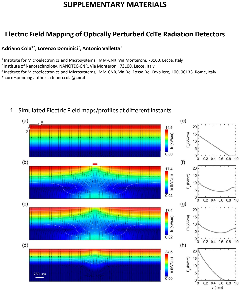
The corresponding profiles at x=0 are also reported aside each map
Simulated Electric Field maps/profiles at different instants Figure S1 Simulated Electric Field maps corresponding to the experimental ones in Fig.1: a) under dark, just before optical irradiation; b) under light, after 5 min of optical irradiation; c) under dark, 2 sec after the light switch-off; d) under dark 15min after the light switch-off. The corres...
-
[35]
The peak of positive space charge under light corresponds to the maximum trapping occurring where the electric field becomes negligible near the cathode
Simulated space charge profiles at different instants Figure S2 Simulated space charge profiles at x=0 (center of optical irradiation) at different instants: under dark just before light (black), under light, after 5 min of optical irradiation (green), under dark, 15 min after the light switch -off (blue). The peak of positive space charge under light cor...
-
[36]
Some relevant parameters of the simulations including those of the 2-level model
Simulation parameters Table S1. Some relevant parameters of the simulations including those of the 2-level model. CdTe Shallow donor level (fully ionized) Concentration Nd 2.8x1013cm-3 Acceptor deep level Energy Ec-Ea 0.725eV Concentration Na 5.8x1013cm-3 Electr. capture cross section σea 1x10-18cm2 Hole capture cross section σha 1.5x10⁻¹⁹cm2 Electron mob...
discussion (0)
Sign in with ORCID, Apple, or X to comment. Anyone can read and Pith papers without signing in.