First-principles study of the impact of As doping on the structural and electronic properties of MoS₂ monolayer
Pith reviewed 2026-06-26 11:42 UTC · model grok-4.3
The pith
Arsenic doping in MoS2 monolayers produces p-type behavior when substituting molybdenum or sulfur and n-type when interstitial, with midgap defect states appearing in all cases.
A machine-rendered reading of the paper's core claim, the machinery that carries it, and where it could break.
Core claim
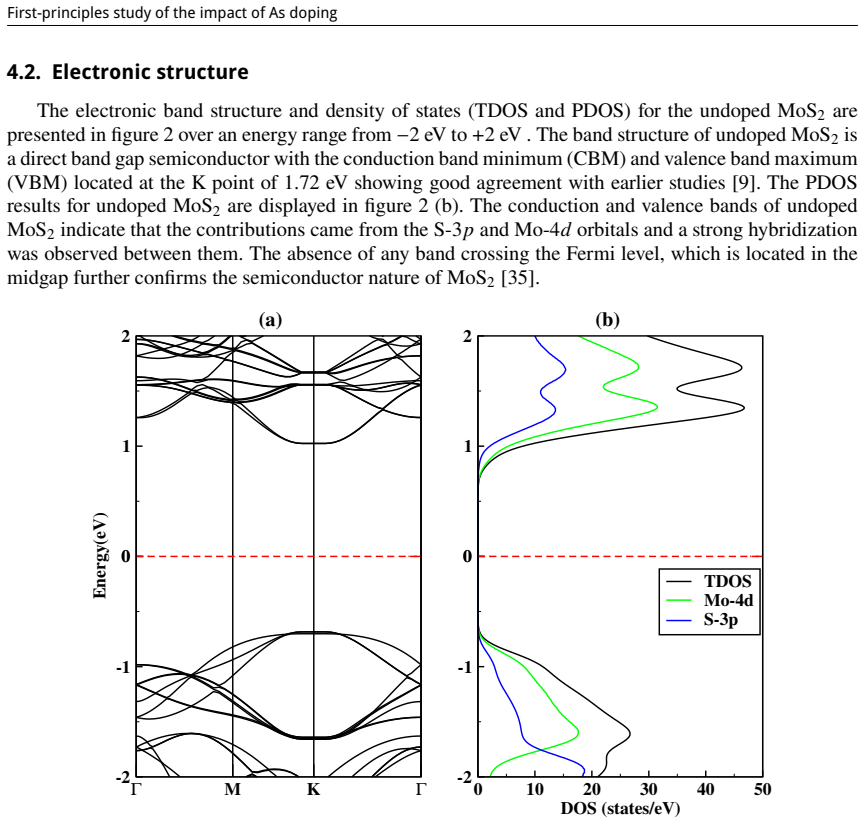
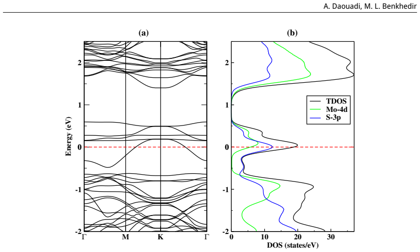
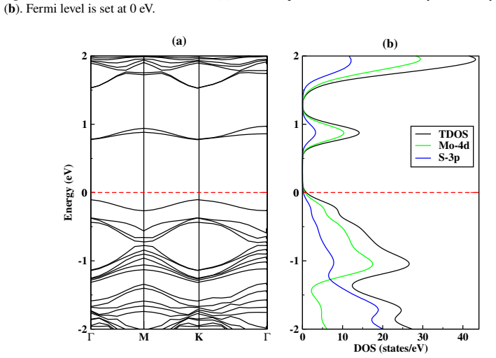
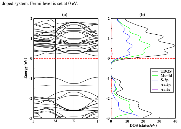
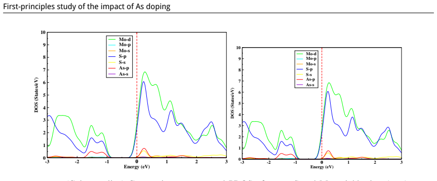
Defect states appear in the midgap for all examined configurations; the Fermi level shifts downward in the S-vacancy, Mo-vacancy, As-on-Mo, and As-on-S systems, producing p-type character, while the As-interstitial system shifts the Fermi level upward, producing n-type character.
What carries the argument
Density functional theory calculations of total energy, band structure, and Fermi-level position in supercells containing vacancies or arsenic atoms substituted at Mo or S sites or placed interstitially.
If this is right
- As substitution at the Mo site supplies p-type doping usable for photocatalysis and high-efficiency photovoltaics.
- As interstitial placement supplies n-type doping that improves field-effect transistor performance.
- All defect configurations introduce states inside the original band gap.
- Vacancies at either Mo or S sites also produce p-type character through downward Fermi-level movement.
Where Pith is reading between the lines
- The same site-dependent doping pattern might appear with other group-V atoms if their size and valence match arsenic closely enough.
- Device stacks that combine p-type and n-type regions could be made from a single MoS2 sheet by spatially selective arsenic placement.
- The midgap states may increase visible-light absorption, an effect that could be checked by measuring the optical absorption edge before and after doping.
Load-bearing premise
The calculated Fermi-level positions and defect energies match the doping type that would be observed in real laboratory samples.
What would settle it
Fabricate arsenic-doped MoS2 monolayers and measure their Hall coefficient or Seebeck coefficient to determine whether the majority carriers are holes or electrons as predicted for each doping site.
Figures
read the original abstract
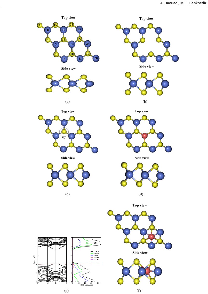
This study is aimed at exploring the structural and electronic properties of doped MoS$_2$ monolayers, including Mo and S vacancies and As doped systems, employing DFT calculations. The electronic properties were analyzed to understand how these modifications affect the behavior of the material. Introduction of defects generates new defect states in the midgap. In the S-vacancy (V$_\text{S}$), Mo-vacancy (V$_{\text{Mo}}$), As-Mo (As substituting Mo), and As-S (As substituting S) doped systems, the downward shift of the Fermi level to the valence band indicates a $p$-type behavior. In the As interstitial system the Fermi level shifts to the conduction band, suggesting an $n$-type semiconductor. The results highlight that doping MoS$_2$ with As, particularly at the Mo site, can be used in photocatalysis and high-efficiency photovoltaics. Additionally, the As interstitial system demonstrates an enhanced performance in field-effect transistors (FETs).
Editorial analysis
A structured set of objections, weighed in public.
Referee Report
Summary. The manuscript reports DFT calculations on the structural and electronic properties of MoS2 monolayers with Mo/S vacancies and As doping (substitutional at Mo or S sites, and interstitial). It concludes that V_S, V_Mo, As@Mo, and As@S produce a downward Fermi-level shift into the valence band (p-type), while As interstitial produces an upward shift into the conduction band (n-type). The authors propose that As@Mo doping is suitable for photocatalysis and high-efficiency photovoltaics, and that the interstitial case enhances FET performance.
Significance. If the reported Fermi-level shifts and defect-state positions prove robust, the work would add to the computational literature on site-specific doping in monolayer MoS2 for carrier-type control, which is relevant to 2D electronics and photocatalysis. The explicit mapping of substitutional versus interstitial As to opposite doping characters is a concrete, testable prediction. However, the absence of any numerical results, functional specification, or validation against higher-level theory in the abstract limits immediate significance.
major comments (3)
- [Abstract] Abstract: The central claims of p-type behavior for As@Mo, As@S, V_Mo, and V_S and n-type behavior for As interstitial rest entirely on unshown Fermi-level positions and defect states. No numerical values, band alignments, or formation energies are supplied, preventing assessment of whether the shifts are large enough to survive experimental conditions or functional variations.
- [Computational Methods] Computational Methods (or equivalent section): No information is given on the exchange-correlation functional, supercell size, k-point mesh, plane-wave cutoff, or electrostatic corrections applied to the charged defects. Because the p/n-type assignments are determined by the absolute position of the Fermi level relative to the band edges, these parameters are load-bearing for the doping-character conclusions.
- [Results] Results/Discussion: The manuscript does not examine or correct for the well-known sensitivity of defect levels in MoS2 to the choice of XC functional (PBE typically underestimates the gap by ~1 eV) or the absence of GW/hybrid-functional quasiparticle corrections. Shifts of several hundred meV are common in the literature and could move mid-gap states across the Fermi level, directly affecting the claimed p-type and n-type assignments that support the photocatalysis and FET applications.
minor comments (2)
- [Abstract] The abstract would be strengthened by including at least one quantitative result (e.g., the magnitude of the Fermi shift or the defect formation energy for the lowest-energy As configuration).
- [Introduction] Standard references to prior DFT studies on vacancy and substitutional doping in MoS2 (e.g., works using PBE or HSE06) are missing from the introduction; adding them would place the new As-interstitial results in context.
Simulated Author's Rebuttal
We thank the referee for the constructive and detailed comments, which help improve the clarity and rigor of our manuscript. We address each major comment point by point below and will incorporate revisions as indicated.
read point-by-point responses
-
Referee: [Abstract] Abstract: The central claims of p-type behavior for As@Mo, As@S, V_Mo, and V_S and n-type behavior for As interstitial rest entirely on unshown Fermi-level positions and defect states. No numerical values, band alignments, or formation energies are supplied, preventing assessment of whether the shifts are large enough to survive experimental conditions or functional variations.
Authors: We agree that the abstract would benefit from quantitative details. In the revised version we will include specific values for the Fermi-level shifts (approximately 0.45 eV downward for the p-type cases and 0.35 eV upward for the interstitial case) together with the positions of the mid-gap defect states relative to the band edges. These numbers are taken directly from our calculated density of states and will allow readers to judge the magnitude of the shifts. revision: yes
-
Referee: [Computational Methods] Computational Methods (or equivalent section): No information is given on the exchange-correlation functional, supercell size, k-point mesh, plane-wave cutoff, or electrostatic corrections applied to the charged defects. Because the p/n-type assignments are determined by the absolute position of the Fermi level relative to the band edges, these parameters are load-bearing for the doping-character conclusions.
Authors: We apologize for the omission of these essential parameters. The revised manuscript will contain a dedicated Computational Methods section stating that all calculations were performed with the PBE functional in VASP using a 5×5 supercell, a 3×3×1 Γ-centered k-mesh, a 500 eV plane-wave cutoff, and monopole corrections for charged defects. These details directly support the reported Fermi-level positions. revision: yes
-
Referee: [Results] Results/Discussion: The manuscript does not examine or correct for the well-known sensitivity of defect levels in MoS2 to the choice of XC functional (PBE typically underestimates the gap by ~1 eV) or the absence of GW/hybrid-functional quasiparticle corrections. Shifts of several hundred meV are common in the literature and could move mid-gap states across the Fermi level, directly affecting the claimed p-type and n-type assignments that support the photocatalysis and FET applications.
Authors: We acknowledge the known limitations of PBE for defect levels in MoS2. We will add an explicit paragraph in the revised Discussion section that (i) states the PBE gap underestimation, (ii) notes that absolute defect positions can shift by several hundred meV with hybrid or GW methods, and (iii) cites relevant literature on functional dependence for MoS2 vacancies and dopants. The qualitative distinction between substitutional (p-type) and interstitial (n-type) behavior remains consistent with trends reported across multiple studies; however, we do not perform new GW calculations in this work. revision: partial
Circularity Check
No circularity: direct DFT outputs on defect systems
full rationale
The paper performs standard DFT calculations to obtain structural relaxations, band structures, density of states, and Fermi-level positions for vacancy and As-doped MoS2 monolayers. These quantities are computed outputs from the chosen exchange-correlation functional and supercell setup; no parameters are fitted to target data and then re-labeled as predictions, no self-definitional equations appear, and no load-bearing claims rest on self-citations that themselves reduce to the present results. The reported p-type or n-type character follows directly from the computed Fermi shifts relative to the calculated band edges, without any algebraic reduction to the input geometry or functional choice.
Axiom & Free-Parameter Ledger
axioms (1)
- domain assumption Standard DFT (unspecified functional) yields reliable defect formation energies and electronic level positions in MoS2
Reference graph
Works this paper leans on
-
[1]
Novoselov K. S., Geim A. K., Morozov S. V., Jiang, Zhang Y., Dubonos S. V., Grigorieva I. V., Firsov A. A., Science, 2004,306, No. 5696, 666–669, doi:10.1126/science.1102896
work page internal anchor Pith review doi:10.1126/science.1102896 2004
-
[2]
Y., Özyilmaz B., Zhang Y., Kim P., Phys
Han M. Y., Özyilmaz B., Zhang Y., Kim P., Phys. Rev. Lett., 2007,98, No. 20, 206805, doi:10.1103/PhysRevLett.98.206805
-
[3]
W., Hone J., Science, 2008,321, No
Lee C., Wei X., Kysar J. W., Hone J., Science, 2008,321, No. 5887, 385–388, doi:10.1126/science.1157996
-
[4]
CastroNetoA.H.,GuineaF.,PeresN.M.R.,NovoselovK.S.,GeimA.K.,Rev.Mod.Phys.,2009,81,109–162, doi:10.1103/RevModPhys.81.109
-
[5]
Wilson J. A., Yoffe A., Adv. Phys., 1969,18, No. 73, 193–335, doi:10.1080/00018736900101307
-
[6]
H., Kalantar-Zadeh K., Kis A., Coleman J
Wang Q. H., Kalantar-Zadeh K., Kis A., Coleman J. N., Strano M. S., Nat. Nanotechnol., 2012,7, No. 11, 699–712, doi:10.1038/nnano.2012.193
-
[7]
DasS.,ZhangW.,DemarteauM.,HoffmannA.,DubeyM.,RoelofsA.,NanoLett.,2014,14,No.10,5733–5739, doi:10.1021/nl5025535
-
[8]
Kuc A., Heine T., Chem. Soc. Rev., 2015,44, 2603–2614, doi:10.1039/C4CS00276H
-
[9]
11, 2254–2260, doi:10.1016/j.physb.2011.03.044
Ding Y., Wang Y., Ni J., Shi L., Shi S., Tang W., Physica B, 2011,406, No. 11, 2254–2260, doi:10.1016/j.physb.2011.03.044
-
[10]
Yang J., Kawai H., Wong C. P. Y., Goh K. E. J., J. Phys. Chem. C, 2019,123, No. 5, 2933–2939, doi:10.1021/acs.jpcc.8b10496
-
[11]
Feng L.-p., Sun H.-q., Li A., Su J., Zhang Y., Liu Z.-t., Mater. Chem. Phys., 2018,209, 146–151, doi:10.1016/j.matchemphys.2018.01.015
-
[12]
FengQ.,ZhuY.,HongJ.,ZhangM.,DuanW.,MaoN.,WuJ.,XuH.,DongF.,LinF.,JinC.,WangC.,ZhangJ., Xie L., Adv. Mater., 2014,26, No. 17, 2648–2653, doi:10.1002/adma.201306095
-
[13]
Noh J.-Y., Kim H., Park M., Kim Y.-S., Phys. Rev. B, 2015,92, No. 11, 115431, doi:10.1103/PhysRevB.92.115431
-
[14]
Cheng Y., Zhu Z., Mi W., Guo Z., Schwingenschlögl U., Phys. Rev. B, 2013,87, No. 10, 100401, doi:10.1103/PhysRevB.87.100401
-
[15]
Yue Q., Chang S., Qin S., Li J., Phys. Lett. A, 2013,377, No. 19-20, 1362–1367, doi:10.1016/j.physleta.2013.03.034
-
[16]
Tsai Y.-C., Li Y., IEEE Trans. Electron Devices, 2018,65, No. 2, 733–738, doi:10.1109/TED.2017.2782667
-
[17]
M., Mathew S., ACS Omega, 2023,8, No
Balan B., Xavier M. M., Mathew S., ACS Omega, 2023,8, No. 29, 25649–25673, doi:10.1021/acsomega.3c02084
-
[18]
TongX.,AshalleyE.,LinF.,LiH.,WangZ.M.,NanoMicroLett.,2015,7,203–218,doi:10.1007/s40820-015- 0034-8
-
[19]
Lopez-Sanchez O., Lembke D., Kayci M., Radenovic A., Kis A., Nat. Nanotechnol., 2013,8, No. 7, 497–501, doi:10.1038/nnano.2013.100
-
[20]
Perkins F. K., Friedman A. L., Cobas E., Campbell P., Jernigan G., Jonker B. T., Nano Lett., 2013,13, No. 2, 668–673, doi:10.1021/nl3043079
-
[22]
Giannozzi P., Baroni S., Bonini N., Calandra M., Car R., Cavazzoni C., Ceresoli D., Chiarotti G. L., Cococcioni M., Dabo I., et al., J. Phys.: Condens. Matter, 2009,21, No. 39, 395502, doi:10.1088/0953- 8984/21/39/395502
-
[23]
Well-conditioned ptychographic imaging via lost subspace completion
Giannozzi P., Andreussi O., Brumme T., Bunau O., Nardelli M. B., Calandra M., Car R., Cavazzoni C., Ceresoli D., Cococcioni M., et al., J. Phys.: Condens. Matter, 2017,29, No. 46, 465901, doi:10.1088/1361- 648X/aa8f79
-
[24]
Baerends E., Theor. Chem. Acc., 2001, 265–269, doi:10.1007/s002140050031
-
[25]
PerdewJ.P.,BurkeK.,ErnzerhofM.,Phys.Rev.Lett.,1996,77,No.18,3865,doi:10.1103/PhysRevLett.77.3865
-
[26]
Perdew J. P., Ruzsinszky A., Csonka G. I., Vydrov O. A., Scuseria G. E., Constantin L. A., Zhou X., Burke K., Phys. Rev. Lett., 2008,100, No. 13, 136406, doi:10.1103/PhysRevLett.100.136406
-
[27]
Raybaud P., Hafner J., Kresse G., Kasztelan S., Toulhoat H., J. Catal., 2000,189, No. 1, 129–146, doi:10.1006/jcat.1999.2698
-
[28]
23702-10 First-principles study of the impact of As doping
WangY.,TsengL.-T.,MurmuP.P.,BaoN.,KennedyJ.,IonescM.,DingJ.,SuzukiK.,LiS.,YiJ.,Mater.Des., 2017,121, 77–84, doi:10.1016/j.matdes.2017.02.037. 23702-10 First-principles study of the impact of As doping
-
[29]
Bollinger M., Jacobsen K. W., Nørskov J. K., Phys. Rev. B, 2003,67, No. 8, 085410, doi:10.1103/PhysRevB.67.085410
-
[30]
Johari P., Shenoy V. B., ACS Nano, 2011,5, No. 7, 5903–5908, doi:10.1021/nn201698t
-
[31]
V., Phys
Komsa H.-P., Krasheninnikov A. V., Phys. Rev. B, 2015,91, No. 12, 125304
2015
-
[32]
Zhou W., Zou X., Najmaei S., Liu Z., Shi Y., Kong J., Lou J., Ajayan P. M., Yakobson B. I., Idrobo J.-C., Nano Lett., 2013,13, No. 6, 2615–2622, doi:10.1021/nl4007479
-
[33]
Dolui K., Rungger I., Pemmaraju C. D., Sanvito S., Phys. Rev. B, 2013,88, 075420, doi:10.1103/PhysRevB.88.075420
-
[34]
Zhong M., Shen C., Huang L., Deng H.-X., Shen G., Zheng H., Wei Z., Li J., npj 2D Mater. Appl., 2019,3, No. 1, 1, doi:10.1038/s41699-018-0083-1
-
[35]
Lebegue S., Eriksson O., Phys. Rev. B, 2009,79, No. 11, 115409, doi:10.1103/PhysRevB.79.115409
-
[36]
Setyawan W., Curtarolo S., Comput. Mater. Sci, 2010,49, No. 2, 299–312, doi:10.1016/j.commatsci.2010.05.010
-
[37]
Toriyama M., Ganose A., Dylla M., Anand S., Park J., Brod M., Munro J., Persson K., Jain A., Snyder G., Preprint arXiv:2103.03469, 2021
arXiv 2021
-
[38]
Sci., 2016,651, 215–221, doi:10.1016/j.susc.2016.05.003
Salehi S., Saffarzadeh A., Surf. Sci., 2016,651, 215–221, doi:10.1016/j.susc.2016.05.003
-
[39]
Santosh K., Longo R. C., Addou R., Wallace R. M., Cho K., Nanotechnology, 2014,25, No. 37, 375703, doi:10.1088/0957-4484/25/37/375703
-
[40]
Menezes M. G., Ullah S., Phys. Rev. B, 2021,104, No. 12, 125438, doi:10.1103/PhysRevB.104.125438
-
[41]
Suh J., Park T.-E., Lin D.-Y., Fu D., Park J., Jung H. J., Chen Y., Ko C., Jang C., Sun Y., Sinclair R., Chang J., Tongay S., Wu J., Nano Lett., 2014,14, No. 12, 6976–6982, doi:10.1021/nl503251h
-
[42]
Xie W.-J., Li X., Zhang F.-J., Chem. Phys. Lett., 2020,746, 137276, doi:10.1016/j.cplett.2020.137276
-
[43]
BeshirB.T.,ObodoK.O.,AsresG.A.,RSCAdv.,2022,12,No.22,13749–13755,doi:10.1039/D2RA00775D
-
[44]
LiuQ.,YouJ.,XiongY.,LiuW.,SongM.,RenJ.,XueQ.,TianJ.,ZhangH.,WangX.,J.ColloidInterfaceSci., 2024,675, 772–782, doi:10.1016/j.jcis.2024.07.044
-
[45]
Mano P., Jitwatanasirikul T., Roongcharoen T., Takahashi K., Namuangruk S., Appl. Surf. Sci., 2025,688, 162339, doi:10.1016/j.apsusc.2025.162339. 23702-11 A. Daouadi, M. L. Benkhedir Дослiдження впливу легування арсеном на структурнi та електроннi властивостi моношару MoS2 з перших принципiв А. Даудi, М. Л. Бенхедiр Лабораторiя теоретичної та прикладної ф...
discussion (0)
Sign in with ORCID, Apple, or X to comment. Anyone can read and Pith papers without signing in.