REVIEW 3 major objections 4 minor 52 references
Broadband Optical Detection using the Spin Seebeck Effect
T0 review · 3 major / 4 minor · reviewed 2026-08-14 · deepseek-v4-flash
Pith's one-line read Spin currents convert absorbed light into a flat photovoltage from 390 to 2200 nm.
desk verdict Solid broadband SSE photodetection demonstration with an internal inconsistency in the SLSSE calibration that likely inflates or misassigns the reported coefficient. read the letter →
The pith
A machine-rendered reading of the paper's core claim, the machinery that carries it, and where it could break.
The reading
What carries the argument
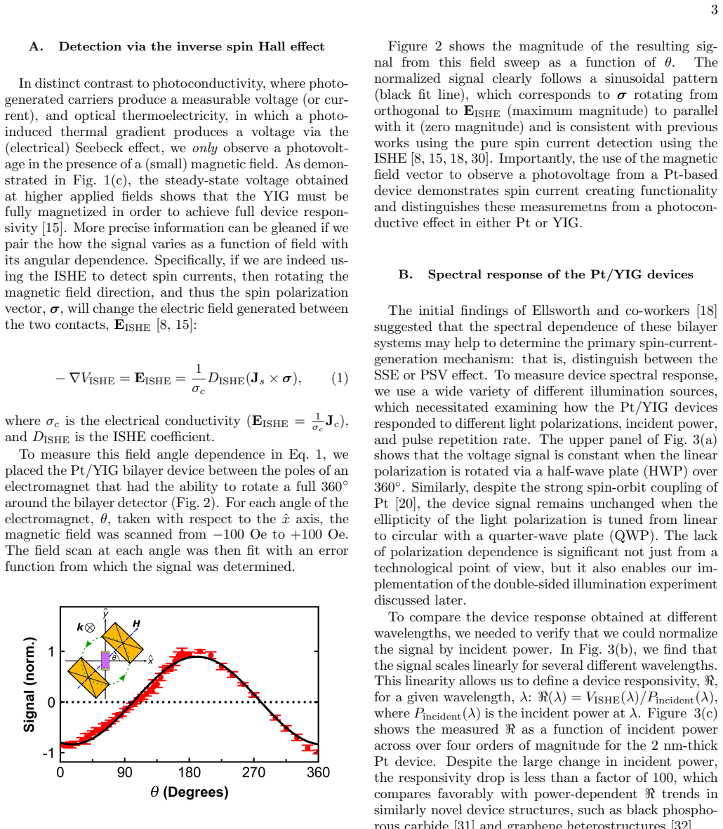
The load-bearing mechanism is the longitudinal spin Seebeck effect: a temperature gradient across the magnetic insulator YIG drives a pure spin current into an adjacent platinum film, and the inverse spin Hall effect in the platinum converts that spin current into a transverse electric field. The named detection relation is E_ISHE = (1/σ_c) D_ISHE (J_s × σ), with the spin polarization σ set by the in-plane magnetic field. The paper's new experimental tool is a field-modulation (amplitude-modulated) measurement in which a small ≈1 G modulation at 13.1 Hz on a swept field gives a derivative signal whose zero marks ∇T = 0, allowing the optical heating contribution to be read as the lateral shift between light-on and light-off curves. This machinery connects the measured photovoltage dynamics directly to platinum thermal response and supports the inference that the bulk SSE, not photocarrier creation, is the detection channel.
What would settle it
Measure the backside GGG temperature directly with a calibrated sensor while sweeping the heat-sink temperature under the same 1190 W/cm² illumination, and compare the zero-crossing temperature of the field-modulated signal with the measured bottom-surface temperature; if they differ, the 11 K optical heating and ∇T = 0.73 K/µm are over- or underestimated.
Extended reading notes
Core claim
The central claim is that the voltage observed when light strikes Pt/YIG/GGG devices is the inverse spin Hall voltage from a thermally generated spin current: absorbed light heats the platinum, a temperature gradient across the YIG launches a spin current, and the platinum converts that spin current into a measurable voltage. The evidence is spectral, dynamic, and geometric: responsivity tracks the Pt absorption coefficient and is nearly featureless from 390 to 2200 nm; the signal is independent of polarization and pulse repetition rate; the temporal response matches platinum heating; the signal disappears where the Pt layer is discontinuous; and edge illumination of the GGG produces almost no response. Using a 13.1 Hz field modulation and a swept heat-sink temperature, the authors locate zero thermal gradient with and without illumination and infer an optical temperature rise of about 11 K, giving ∇T ≈ 0.73 K/µm and SLSSE ≈ 60 ± 7.8 nV/K. They further argue that the photo-spin-voltaic mechanism is negligible because its estimated contribution (~4.9 nV) is three orders of magnitude below the measured signal.
Load-bearing premise
The field-modulation calibration assumes the GGG backside sits at the copper heat-sink temperature and that the unilluminated platinum surface is at 20 °C, so the zero of the integrated amplitude-modulated signal marks zero temperature gradient across the YIG; a thermal resistance between GGG and the heat sink, or a different light-off Pt temperature, would shift the inferred optical heating and the 60 nV/K coefficient.
Editorial extensions
If this is right
- A single Pt/YIG detector can respond uniformly from 390 to 2200 nm, spanning the silicon and InGaAs ranges without a semiconductor band-gap cutoff.
- Because the response follows platinum absorption, extending the operating range further into the infrared is plausible whenever the Pt film still absorbs.
- The field-modulation method gives a direct, sample-specific calibration of optical heating, which can be used to extract SSE coefficients in other metal/insulator bilayers.
- Thinner platinum films yield higher responsivity (more than an order of magnitude from 6 to 2 nm), so interface and thickness engineering are the levers for improving sensitivity.
- The estimated SSE coefficient is consistent with prior Pt/YIG measurements, and published routes for enhancing SSE efficiency imply larger photovoltages should be attainable.
Reading between the lines
- If the detection is purely thermal, the spectral range is bounded only by Pt absorption and not by any electronic resonance, so the same architecture could be tested at longer infrared wavelengths or with different high-absorption metals.
- The calibration's dependence on the assumption T_GGG ≈ T_Cu could be tested by inserting a known thermal resistance between the GGG and heat sink; a shift of the zero crossing would quantify the systematic error.
- A follow-on direct comparison of measured Pt film temperature rise (via resistance) with the 11 K inferred gradient would separate bulk thermal diffusion effects from interfacial Kapitza resistance and sharpen the bulk-versus-interfacial SSE assignment.
Signed reviews
Editorial analysis
A structured set of objections, weighed in public.
Referee Report
Summary. The manuscript reports that Pt/YIG/GGG bilayers produce a photovoltage across a wide wavelength range (390–2200 nm) under illumination, and argues that the signal arises from the longitudinal spin Seebeck effect (LSSE). The authors show that the spectral responsivity is roughly flat and correlates with the Pt absorption coefficient (data shown to 1000 nm), that the photovoltage is independent of light polarization, scales linearly with average power and repetition rate, and matches the thermal dynamics of the Pt film. They introduce a field-amplitude-modulation technique to infer the optically induced temperature difference across the YIG (about 11 K at 1190 W/cm², 405 nm) and combine this with the measured electric field (3.457 µV across 80 µm) to estimate an LSSE coefficient of 60 ± 7.8 nV/K. They also estimate the competing photo-spin-voltaic effect to be negligible. The paper claims a new broadband optical detection mechanism based solely on spin-current generation and detection.
Significance. If the conclusions hold, this work demonstrates a conceptually new type of broadband photodetector that operates via thermally generated spin currents rather than photocarriers, with potential advantages for infrared detection and spin-caloritronic devices. The field-modulation null method is a useful addition to the spin-Seebeck measurement toolkit, and the paper includes a commendable set of cross-checks: polarization independence, power linearity, repetition-rate insensitivity, front/back illumination symmetry, edge illumination, Pt-removal spatial mapping, and the null-point shift itself. However, the quantitative calibration of the reported LSSE coefficient contains an internal inconsistency with Appendix B, and the thermal-resistance assumption underlying the temperature-gradient measurement is not quantified. These issues put the headline numerical value on shaky ground, although the qualitative spin-Seebeck-based detection claim is supported by the ensemble of measurements.
major comments (3)
- [§II F and Appendix B] The reported calibration of the LSSE coefficient is internally inconsistent. In §II F, the authors state that an intensity of 1190 W/cm² (405 nm) generates a VISHE of 3.457 µV and use this to obtain EISHE = 43 mV/m and SLSSE = 60 ± 7.8 nV/K. Appendix B, however, uses a 405 nm beam with 18 mW and 80 µm diameter (intensity ≈ 3.6 MW/m² = 360 W/cm²) and cites the same observed signal, 3.457 µV, for the 2 nm Pt device. Since 1190 W/cm² is a factor of 3.3 larger than 360 W/cm², a linear detector (Fig. 3b) would produce roughly 11.5 µV at the higher intensity, leading to EISHE ≈ 143 mV/m and SLSSE ≈ 200 nV/K. If the authors instead measured 3.457 µV at 360 W/cm², then the statement in §II F that 'this intensity' (1190 W/cm²) generates 3.457 µV is incorrect. The manuscript must clarify the exact power/intensity used in each measurement, reconcile the two pairs, and recompute the LSSE coefficient and its uncertainty accordingly.
- [§II F, Eq. (for ∇T)] The field-modulation null method rests on the assumption that TGGG ≈ TCu, both with and without illumination. In the light-off state, there is no heat flow, so TGGG = TCu is reasonable. In the light-on state, however, heat flows from the Pt through the YIG and GGG to the copper sink, and any thermal resistance between GGG and the sink makes TGGG exceed TCu. The zero-crossing shift then equals ΔT_optical minus QR_th, not ΔT_optical itself, so the inferred 11 K and the derived SLSSE would be systematically biased. The claim that 'the only thing changing between the curves is the presence of an additional heating source' is therefore incomplete. The sensitivity of the result to the GGG–sink thermal resistance should be quantified with a thermal model or a direct temperature measurement at the GGG surface, and this contribution should be included in the uncertainty budget.
- [Abstract and Fig. 3(e)] The abstract states that the device responsivity 'closely following the Pt absorption coefficient' across 390–2200 nm, but the Pt absorption coefficient is only measured and displayed from 390 to 1000 nm. The agreement between the spectral response and α_Pt is therefore demonstrated only over part of the claimed range. To support the broadband-correlation claim, the authors should either extend the absorption-coefficient measurement to 2200 nm or clearly state that the correlation is established only in the 390–1000 nm range and that the flat responsivity at longer wavelengths is consistent with an expected flat α_Pt.
minor comments (4)
- [Fig. 3(c) and Sec. II B] The statement that the responsivity drop is 'less than a factor of 100' over four orders of magnitude of incident power appears inconsistent with the claim of linear power scaling in Fig. 3(b). If the voltage were strictly linear, the responsivity would be constant. Please clarify the power range over which linearity holds and reconcile the apparent sublinearity in Fig. 3(c).
- [Sec. II D vs. Sec. II F/Conclusion] In Sec. II D the authors state that 'we still cannot conclusively determine whether the SSE and/or PSV effect is the dominant spin-current generation mechanism,' but later in Sec. II F and the Conclusion they conclude that the signal comes predominantly from the bulk SSE. This wording is confusing; please revise to reflect the evidence presented in Appendix B.
- [Sec. II C] The symbol 'SSSE' appears in the sentence 'theoretical models of how SSSE varies with Pt thickness'; this appears to be a typo for the spin Seebeck coefficient (SLSSE or SSE).
- [Appendix B] The spin Hall angle is stated to range 'from 10^-4 to 100'; this likely should be 10^-4 to 1.0 (or another intended bound). Please correct the typographical representation of the exponent.
Circularity Check
No significant circularity; the S_LSSE value is a measured ratio and the amplitude-modulated temperature calibration is a null measurement.
full rationale
The central derivation is self-contained and does not reduce a prediction to an input. The spectral responsivity ℜ(λ) is measured directly and compared with a directly measured Pt absorption coefficient; no fitted parameter is reused to generate ℜ. The amplitude-modulation calibration in Sec. II F is a null measurement: the 11 K optically induced temperature difference is obtained from the shift in the zero-crossing temperature of the integrated AM signal between light-off and light-on conditions, not from the S_LSSE value or from any fitted constant. S_LSSE = 60 ± 7.8 nV/K is then a ratio of two measured quantities (EISHE = 43 mV/m and ∇T = 0.73 K/µm), i.e., a definition of a material coefficient rather than a prediction derived from it. The PSV estimate in Appendix B uses the authors' prior model (Ref. 18), but that model's wavelength dependence is tested against the measured flat spectrum and found wanting, and the PSV exclusion is corroborated by independent GGG/edge-illumination, thickness-dependence, and dynamics measurements; hence the self-citation is not load-bearing. The apparent inconsistency between Sec. II F (3.457 µV at 1190 W/cm2) and Appendix B (same 3.457 µV at 18 mW through an 80-µm spot, i.e., ~360 W/cm2) is a quantitative calibration concern, not a circularity: neither number is derived from the other, and the disagreement would only shift the reported S_LSSE, not make the central mechanism claim tautological. No step in the paper was found in which an output is equal to an input by construction.
Assumptions & free parameters
free parameters (4)
- αTC_Pt =
2.39e-4 K^-1
- d0 (proximity thickness for PSV estimate) =
1 Å
- θ_SH (spin Hall angle for PSV estimate) =
0.1
- ε''↑ - ε''↓ (spin-dependent absorptive dielectric difference for PSV estimate) =
0.5
assumptions (5)
- domain assumption VISHE is proportional to Js and to the thermal gradient across YIG (VISHE ∝ ∇T).
- domain assumption TGGG ≈ TCu and TPt ≈ room temperature when light is off.
- domain assumption Optical absorption in YIG and GGG is negligible compared to Pt for the excitation geometry.
- domain assumption Bulk LSSE dominates over anomalous Nernst, proximity, and interfacial SSE effects.
- standard math The ISHE relation E_ISHE = (1/σ_c) D_ISHE (Js × σ) holds for the Pt film.
Cite this review
Pith. "Pith review of Broadband Optical Detection using the Spin Seebeck Effect." pith.science (2026). https://pith.science/paper/GP3C3OVY
@misc{pith2026190810472,
  author       = {Pith},
  title        = {Pith review of: Broadband Optical Detection using the Spin Seebeck Effect},
  year         = {2026},
  howpublished = {\url{https://pith.science/paper/GP3C3OVY}},
  note         = {Machine review of arXiv:1908.10472}
}
read the original abstract
The generation, control, and detection of spin currents in solid-state devices are critical for Joule-heating minimization, spin-based computation, and electrical energy generation from thermal gradients. Although incorporation of spin functionality into technologically important architectures is still in its infancy, advantages over all-electric devices are increasingly becoming clear. Here, we utilize the spin Seebeck effect (SSE) in Pt/Y3Fe5O12 devices to detect light from 390 to 2200 nm. We find the device responsivity is remarkably flat across this technologically important wavelength range, closely following the Pt absorption coefficient. As expected from a SSE-generation mechanism, we observe that the photovoltage and Pt heating dynamics are in strong agreement. To precisely determine the optically created thermal gradient produced from a point-like heat source, we introduce a field-modulation method for measuring the SSE. Our results show broadband optical detection can be performed with devices based solely on spin current generation and detection.
Figures


Figures from the paper (4 more)


Reference graph
Works this paper leans on
-
[1]
T. Jungwirth, J. Wunderlich, and K. Olejn´ ık, “Spin Hall effect devices,” Nature Mater. 11, 382 (2012)
work page 2012
-
[2]
G. E. W. Bauer, E. Saitoh, and B. J. van Wees, “Spin caloritronics,” Nature Mater. 11, 391 (2012)
work page 2012
-
[3]
Spintronics: A spin- based electronics vision for the future,
S. A. Wolf, D. D. Awschalom, R. A. Buhrman, J. M. Daughton, S. von Molnar, M. L. Roukes, A. Y. Chtchelkanova, and D. M. Treger, “Spintronics: A spin- based electronics vision for the future,” Science 294, 1488–1495 (2001)
work page 2001
-
[4]
Spintronics: Fundamentals and applications,
I. ˘Zuti´ c, J. Fabian, and S. Das Sarma, “Spintronics: Fundamentals and applications,” Rev. Mod. Phys. 76, 323 (2004)
work page 2004
-
[5]
Optically switched magnetism in photo- voltaic perovskite CH 3NH3(Mn:Pb)I3,
B. N´ afr´ adi, P. Szirmai, M. Spina, H. Lee, O. V. Yazyev, A. Arakcheeva, D. Chernyshov, M. Gibert, L. Forr´ o, and E. Horv´ ath, “Optically switched magnetism in photo- voltaic perovskite CH 3NH3(Mn:Pb)I3,” Nature Comm. 7, 13406 (2016)
work page 2016
-
[6]
Observation of the spin Seebeck effect,
K. Uchida, S. Takahashi, K. Harii, J. Ieda, W. Koshibae, K. Ando, S. Maekawa, and E. Saitoh, “Observation of the spin Seebeck effect,” Nature 455, 778 (2008)
work page 2008
-
[7]
dc effect in ferromag- netic resonance: Evidence of the spin-pumping effect?
A. Azevedo, L. H. Vilela Le˜ ao, R. L Rodriguez-Suarez, A. B. Oliveira, and S. M. Rezende, “dc effect in ferromag- netic resonance: Evidence of the spin-pumping effect?” J. Appl. Phys. 97, 10C715 (2005)
work page 2005
-
[8]
Con- version of spin current into charge current at room tem- perature: Inverse spin-Hall effect,
E. Saitoh, M. Ueda, H. Miyajima, and G. Tatara, “Con- version of spin current into charge current at room tem- perature: Inverse spin-Hall effect,” Appl. Phys. Lett. 88, 182509 (2006)
work page 2006
Show all 52 references
-
[9]
Spin Hall effect,
J. E. Hirsch, “Spin Hall effect,” Phys. Rev. Lett. 83, 1834 (1999)
1999
-
[10]
Observation of the spin Hall effect in semi- conductors,
Y. K. Kato, R. C. Myers, A. C. Gossard, and D. D. Awschalom, “Observation of the spin Hall effect in semi- conductors,” Science 306, 1910 (2004)
2004
-
[11]
Direct electronic measurement of the spin Hall effect,
S. O. Valenzuela and M. Tinkham, “Direct electronic measurement of the spin Hall effect,” Nature 442, 176 (2006)
2006
-
[12]
Spin- current-driven thermoelectric coating,
A. Kirihara, K. Uchida, Y. Kajiwara, M. Ishida, Y. Naka- mura, T. Manako, E. Saitoh, and S. Yorozu, “Spin- current-driven thermoelectric coating,” Nature Mater. 11, 686 (2012)
2012
-
[13]
Thermal spin pumping and magnon-phonon-mediated spin-Seebeck effect,
K. Uchida, T. Ota, H. Adachi, J. Xiao, T. Nonaka, Y. Ka- jiwara, G. E. W. Bauer, S. Maekawa, and E. Saitoh, “Thermal spin pumping and magnon-phonon-mediated spin-Seebeck effect,” J. Appl. Phys. 111, 103903 (2012)
2012
-
[14]
Observation of the spin-Seebeck effect in a ferromagnetic semiconductor,
C. M. Jaworski, J. Yang, S. Mack, D. D. Awschalom, J. P. Heremans, and R. C. Myers, “Observation of the spin-Seebeck effect in a ferromagnetic semiconductor,” Nature Mater. 9, 898 (2010)
2010
-
[15]
Observation of longitu- dinal spin-Seebeck effect in magnetic insulators,
K. Uchida, H. Adachi, T. Ota, H. Nakayama, S. Maekawa, and E. Saitoh, “Observation of longitu- dinal spin-Seebeck effect in magnetic insulators,” Appl. Phys. Lett. 97, 172505 (2010)
2010
-
[16]
Longitu- dinal spin-Seebeck effect in sintered polycrystalline (Mn, Zn)Fe2O4,
K. Uchida, T. Nonaka, T. Ota, and E. Saitoh, “Longitu- dinal spin-Seebeck effect in sintered polycrystalline (Mn, Zn)Fe2O4,” Appl. Phys. Lett. 97, 262504 (2010)
2010
-
[17]
Spin See- beck insulator,
K. Uchida, J. Xiao, H. Adachi, J. Ohe, S. Takahashi, J. Ieda, T. Ota, Y. Kajiwara, H. Umezawa, H. Kawai, G. E. W. Bauer, S. Maekawa, and E. Saitoh, “Spin See- beck insulator,” Nature Mater. 9, 894 (2010)
2010
-
[18]
Photo-spin-voltaic effect,
D. Ellsworth, L. Lei, J. Lan, H. Chang, P. Li, Z. Wang, J. Hu, B. Johnson, Y. Bian, J. Xiao, R. Wu, and M. Wu, “Photo-spin-voltaic effect,” Nature Phys. 12, 861 (2016)
2016
-
[19]
Spin-voltaic effect and its impli- cations,
I. ˘Zuti´ c and J. Fabian, “Spin-voltaic effect and its impli- cations,” Materials Trans. 44, 2062 (2003)
2003
-
[20]
Room-temperature reversible spin Hall ef- fect,
T. Kimura, Y. Otani, T. Sato, S. Takahashi, and S. Maekawa, “Room-temperature reversible spin Hall ef- fect,” Phys. Rev. Lett. 98, 156601 (2007)
2007
-
[21]
Imaging magnetization structure and dynamics in ul- trathin Y3Fe5O12/Pt bilayers with high sensitivity using the time-resolved longitudinal spin Seebeck effect,
J. M. Bartell, C. L. Jermain, S. V. Aradhya, J. T. Brangham, F. Yang, D. C. Ralph, and G. D. Fuchs, “Imaging magnetization structure and dynamics in ul- trathin Y3Fe5O12/Pt bilayers with high sensitivity using the time-resolved longitudinal spin Seebeck effect,” Phys. Rev. Appl...
2017
-
[22]
Spin current generated by thermally driven ultrafast demag- netization,
G-M. Choi, B-C. Min, K-J. Lee, and D. G. Cahill, “Spin current generated by thermally driven ultrafast demag- netization,” Nature Comm. 5, 4334 (2014)
2014
-
[23]
Picosecond spin Seebeck effect,
J. Kimling, G.-M. Choi, J. T. Brangham, T. Matalla- Wagner, T. Huebner, T. Kuschel, F. Yang, and D. G. Cahill, “Picosecond spin Seebeck effect,” Phys. Rev. Lett. 118, 057201 (2017)
2017
-
[24]
Optical detection of transverse spin- Seebeck effect in permalloy film using Sagnac interfer- ometer microscopy,
R. McLaughlin, D. Sun, C. Zhang, M. Groesbeck, and Z. V. Vardeny, “Optical detection of transverse spin- Seebeck effect in permalloy film using Sagnac interfer- ometer microscopy,” Phys. Rev. B 95, 180401(R) (2017)
2017
-
[25]
Giant anomalous Nernst effect and quantum- critical scaling in a ferromagnetic semimetal,
A. Sakai, Y. P. Mizuta, A. A. Nugroho, R. Sihomb- ing, T. Koretsune, M.-T. Suzuki, N. Takemori, R. Ishii, D. Nishio-Hamane, R. Arita, P. Goswami, and S. Nakat- suji, “Giant anomalous Nernst effect and quantum- critical scaling in a ferromagnetic semimetal,” Nature Phys. 14, 1119 (2016)
2016
-
[26]
Trans- port magnetic proximity effects in platinum,
S. Y. Huang, X. Fan, D. Qu, Y. P. Chen, W. G. Wang, J. Wu, T. Y. Chen, J. Q. Xiao, and C. L. Chien, “Trans- port magnetic proximity effects in platinum,” Phys. Rev. Lett. 109, 107204 (2012)
2012
-
[27]
Separation of longitudinal spin Seebeck effect from anomalous Nernst effect: Determination of origin of transverse thermoelectric voltage in metal/insulator junctions,
T. Kikkawa, K. Uchida, S. Daimon, Y. Shiomi, H. Adachi, Z. Qui, D. Hou, X.-F. Jin, S. Maekawa, and E. Saitoh, “Separation of longitudinal spin Seebeck effect from anomalous Nernst effect: Determination of origin of transverse thermoelectric voltage in metal/insulator junctions,”...
2013
-
[28]
Ab- sence of anomalous Nernst effect in spin Seebeck effect fo Pt/YIG,
B. F. Miao, S. Y. Huang, D. Qu, and C. L. Chien, “Ab- sence of anomalous Nernst effect in spin Seebeck effect fo Pt/YIG,” AIP Advances 6, 015018 (2016)
2016
-
[29]
Role of bulk- magnon transport in the temporal evolution of the lon- gitudinal spin-Seebeck effect,
M. Agrawal, V. I. Vasyuchka, A. A. Serga, A. Kirihara, P. Pirro, T. Langer, M. B. Jungfleisch, A. V. Chumak, E. Th. Papioannou, and B. Hillebrands, “Role of bulk- magnon transport in the temporal evolution of the lon- gitudinal spin-Seebeck effect,” Phys. Rev. B 89, 224414 (2014)
2014
-
[30]
Scaling of spin Hall angle in 3d, 4d, and 5d metals Y 3Fe5O12/metal spin pumping,
H. L. Wang, C. H. Du, Y. Pu, R. Adur, P. C. Hammel, and F. Y. Yang, “Scaling of spin Hall angle in 3d, 4d, and 5d metals Y 3Fe5O12/metal spin pumping,” Phys. Rev. Lett. 112, 197201 (2014)
2014
-
[31]
A black phosphorus carbide infrared phototransistor,
W. C. Tan, L. Huang, R. J. Ng, L. Wang, D. M. N. Hasan, T. J. Duffin, K. S. Kumar, C. A. Nijhuis, C. Lee, and K.-W. Ang, “A black phosphorus carbide infrared phototransistor,” Adv. Mater. 30, 1705039 (2018)
2018
-
[32]
Broadband photovoltaic detectors based on an atomically thin heterostructure,
M. Long, E. Liu, P. Wang, A. Gao, H. Xia, W. Luo, B. Wang, J. Zeng, Y. Fu, K. Xu, W. Zhou, Y. Lv, S. Yao, M. Lu, Y. Chen, Z. Ni, Y. You, X. Zhang, S. Qin, Y. Shi, W. Hu, D. Xing, and F. Miao, “Broadband photovoltaic detectors based on an atomically thin heterostructure,” 12 Na...
2016
-
[33]
Fast and broadband photoresponse of few-layer black phosphorous field-effect transistors,
M. Buscema, D. J. Groenendijk, S. I. Blanter, G. A. Steele, H. S. J. van der Zant, and A. Castellanos-Gomez, “Fast and broadband photoresponse of few-layer black phosphorous field-effect transistors,” Nano Lett.14, 3347 (2014)
2014
-
[34]
Ultrasensitive and broadband MoS 2 photode- tector driven by ferroelectrics,
X. Wang, P. Wang, J. Wang, W. Hu, X. Zhou, N. Guo, H. Huang, S. Sun, H. Shen, T. Lin, M. Tang, L. Liao, A. Jiang, J. Sun, X. Meng, X. Chen, W. Lu, and J. Chu, “Ultrasensitive and broadband MoS 2 photode- tector driven by ferroelectrics,” Adv. Mater. 27, 6575 (2015)
2015
-
[35]
Graphene photodetectors with ultra-broadband and high responsivity at room temperature,
C-H. Liu, Y-C. Chang, T. B. Norris, and Z. Zhong, “Graphene photodetectors with ultra-broadband and high responsivity at room temperature,” Nature Nan- otech. 9, 273 (2014)
2014
-
[36]
Pla- nar carbon nanotube-graphene hybrid films for high- performance broadband photodetectors,
Y. Liu, F. Wang, X. Wang, X. Wang, E. Flahaut, X. Liu, Y. Li, X. Wang, Y. Xu, Y. Shi, and R. Zhang, “Pla- nar carbon nanotube-graphene hybrid films for high- performance broadband photodetectors,” Nature Comm. 6, 8589 (2015)
2015
-
[37]
Resonant terahertz detection using graphene plasmons,
D. A. Bandurin, D. Svintsov, I. Gayduchenko, S. G. Xu, A. Principi, M. Moskotin, I. Tretyakov, D. Yagodkin, S. Zhukov, T. Taniguchi, K. Watanabe, I. V. Grigorieva, M. Polini, G. N. Goltsman, A. K. Geim, and G. Fe- dorov, “Resonant terahertz detection using graphene plasmons,” ...
2018
-
[38]
Spin Seebeck coefficient enhancement by using Ta50W50 alloy and YIG/Ru interface,
H. Yuasa, F. Nakata, R. Nakamura, and Y. Kurokawa, “Spin Seebeck coefficient enhancement by using Ta50W50 alloy and YIG/Ru interface,” J. Phys. D: Appl. Phys.51, 134002 (2018)
2018
-
[39]
Spin Seebeck voltage enhancement by Mn system met- als insertion at the interface between YIG and nonmag- netic layer,
F. Nakata, T. Niimura, Y. Kurokawa, and H. Yuasa, “Spin Seebeck voltage enhancement by Mn system met- als insertion at the interface between YIG and nonmag- netic layer,” Japanese Journal of Appl. Phys.58, SBBI04 (2019)
2019
-
[40]
Experimental test of the spin mixing interface conductivity concept,
M. Weiler, M. Althammer, M. Schreier, J. Lotze, M. Pernpeintner, S. Meyer, H. Huebl, R. Gross, A. Kamra, J. Xiao, Y.-T. Chen, H. Jiao, G. E. W. Bauer, and S. T. B. Goennenwein, “Experimental test of the spin mixing interface conductivity concept,” Phys. Rev. Lett. 111, 176601 (2013)
2013
-
[41]
Surface sensitivity of the spin Seebeck effect,
A. Aqeel, I. J. Vera-Marun, B. J. van Wees, and T. T. M. Palstra, “Surface sensitivity of the spin Seebeck effect,” J. Appl. Phys. 116, 153705 (2014)
2014
-
[42]
Precise determination of the temperature gradients in laser-irradiated ultrathin magnetic layers for the analysis of thermal spin current,
S. Surabhi, D.-J. Kim, P. C. Van, V. D. Quoc, J.-K. Kim, S. W. Lee, R. Kuchi, J.-W. Lee, S.-G. Yoon, J. Choi, B.-G. Park, and J.-R. Jeong, “Precise determination of the temperature gradients in laser-irradiated ultrathin magnetic layers for the analysis of thermal spin current...
2018
-
[43]
The absorption spectra of Y3Fe5O12 and Y3Ga5O12:Fe3+ to 5.5 eV,
G. B. Scott and J. L. Page, “The absorption spectra of Y3Fe5O12 and Y3Ga5O12:Fe3+ to 5.5 eV,” phys. stat. sol. (b) 79, 203 (1977)
1977
-
[44]
Light-induced phase and amplitude gratings in cen- trosymmetric gadolinium gallium garnet doped with cal- cium,
M. A. Ellabban, M. Fally, R. A. Rupp, and L. Kov´ acs, “Light-induced phase and amplitude gratings in cen- trosymmetric gadolinium gallium garnet doped with cal- cium,” Optics Express 14, 593 (2006)
2006
-
[45]
Microstruc- ture and temperature coefficient of resistance of platinum films,
J. Zhang, Y. Nagao, S. Kuwano, and Y. Ito, “Microstruc- ture and temperature coefficient of resistance of platinum films,” Japanese Journal of Appl. Phys. 36, 834 (1997)
1997
-
[46]
General physical prop- erties,
W. F. Gale and T. C. Totemeier, “General physical prop- erties,” in Smithells Metals Reference Book (Elsevier,
-
[47]
Resistivity and temperature coefficient of thin metal films with rough surface,
Y. Namba, “Resistivity and temperature coefficient of thin metal films with rough surface,” Japanese Journal of Appl. Phys. 9, 1326 (1970)
1970
-
[48]
Evaluation of thermal gradients in longitudinal spin Seebeck effect mea- surements,
A. Sola, M. Kuepferling, V. Basso, M. Pasquale, T. Kikkawa, K. Uchida, and E. Saitoh, “Evaluation of thermal gradients in longitudinal spin Seebeck effect mea- surements,” J. Appl. Phys. 117, 17C510 (2015)
2015
-
[49]
Lon- gitudinal spin Seebeck coefficient: heat flux vs. temper- ature difference method,
A. Sola, P. Bougiatioti, M. Kuepferling, D. Meier, G. Reiss, M. Pasquale, T. Kuschel, and V. Basso, “Lon- gitudinal spin Seebeck coefficient: heat flux vs. temper- ature difference method,” Sci. Rep. 7, 46752 (2017)
2017
-
[50]
Silicon nanowires as efficient thermoelectric materials,
A. I. Boukai, Y. Bunimovich, J. Tahir-Kheli, J.-K. Yu, W. A. Goddard III, and J. R. Heath, “Silicon nanowires as efficient thermoelectric materials,” Nature 451, 168 (2008)
2008
-
[51]
Ultra-high Seebeck coefficient and low thermal conductivity of a centimeter-sized perovskite single crys- tal acquired by a modified fast growth method,
T. Ye, X. Wang, X. Li, A. Q. Yan, S. Ramakrishna, and J. Xu, “Ultra-high Seebeck coefficient and low thermal conductivity of a centimeter-sized perovskite single crys- tal acquired by a modified fast growth method,” J. Mater. Chem. C 5, 1255 (2017)
2017
-
[52]
Gi- ant spin hall effect in perpendicularly spin-polarized FePt/Au devices,
T. Seki, Y. Hasegawa, S. Mitani, S. Takahashi, H. Ima- mura, S. Maekawa, J. Nitta, and K. Takanashi, “Gi- ant spin hall effect in perpendicularly spin-polarized FePt/Au devices,” Nature Mater. 7, 125 (2008)
2008
Reviewed August 14, 2026 · model on record in the stance chip above.
Discussion (0). Continue with ORCID to comment.