REVIEW 3 major objections 5 minor 1 cited by
Epitaxial growth and transport properties of a metallic altermagnet CrSb on a GaAs (001) substrate
T0 review · 3 major / 5 minor · reviewed 2026-08-08 · deepseek-v4-flash
Pith's one-line read A one-monolayer FeSb template makes single-crystalline altermagnet CrSb grow on GaAs(001), with -1.0 percent compressive strain.
desk verdict Worth refereeing: a credible CrSb-on-GaAs(001) growth route with one unproven interface — ask for composition data before trusting the transport as intrinsic. read the letter →
The pith
A machine-rendered reading of the paper's core claim, the machinery that carries it, and where it could break.
The reading
What carries the argument
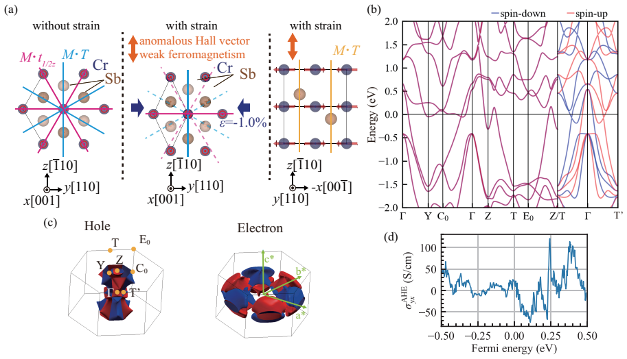
The mechanism that carries the growth is the 1-ML FeSb template: FeSb has the same NiAs-type crystal structure as CrSb and nearly the same lattice constants, so it seeds the (1-10) plane on AlAs/GaAs(001) and suppresses competing (1-11) and (1-12) orientations. The interface then settles into a 7-to-5 registry, with seven GaAs/AlAs (1-10) spacings matching five CrSb (001) spacings, producing an atomically abrupt interface and the measured -1.0% strain. On the physics side, the load-bearing symmetry argument is that this strain removes four of the mirror and glide operations in CrSb, allowing a T-odd axial vector, namely the anomalous Hall vector and a possible weak ferromagnetic moment, along CrSb[1-10]; the first-principles Wannier calculation supplies the magnitude, about 20 S/cm, that transport did not detect.
What would settle it
An atomically resolved composition profile across the CrSb/FeSb/AlAs stack (for example an EELS or EDS line scan) would settle it: Fe present inside the 30-nm CrSb beyond the intended monolayer, or CrSb (1-11) and (1-12) XRD peaks reappearing in a repeat growth, would falsify the claim that the FeSb template alone produces single-crystalline, stoichiometric, strain-engineered CrSb.
Extended reading notes
Core claim
The central claim is that inserting a 1-ML FeSb (1-10) layer between a 5-nm AlAs buffer and CrSb turns an otherwise polycrystalline or misoriented growth into a single-crystalline CrSb (1-10) film on GaAs(001), with CrSb[110] parallel to GaAs[110] and CrSb[001] parallel to GaAs[1-10]. The film is compressively strained by $\varepsilon = -1.0\%$ along CrSb[110] (with $\varepsilon$ defined relative to the regular hexagonal plane), which partially breaks the glide and magnetic-mirror symmetries that forbid T-odd axial vectors in bulk CrSb. First-principles band-structure and Berry-curvature calculations using the measured lattice constants give a sizable anomalous Hall conductivity around 20 S/cm, but the measured Hall resistivity contains no hysteretic anomalous component; instead, a two-carrier fit describes it with electron and hole carriers and indicates a semimetal with carrier densities in the $10^{20}\,\mathrm{cm}^{-3}$ range and mobilities around $10^4\,\mathrm{cm}^2/\mathrm{V\,s}$. The authors interpret the missing AHE as likely meaning the N\'eel vector has not been reversed in this strain state, not that the altermagnetic order is absent.
Load-bearing premise
The 1-ML FeSb layer must act only as a structural template, staying at the interface; if Fe diffuses into CrSb during growth or annealing, the film becomes a Fe-doped alloy and the reported strain, symmetry, and transport interpretations would need revision.
Editorial extensions
If this is right
- CrSb can be integrated on the widely used GaAs(001) platform without a lattice-matched substrate, because the FeSb/AlAs buffer controls the orientation rather than the lattice matching.
- The measured -1.0% compressive strain breaks the symmetry that forbids the anomalous Hall response in bulk CrSb, making this film recipe a platform for testing strain-induced N\'eel-vector reversal.
- The two-carrier transport analysis says the film is a semimetal with coexisting electrons and holes, with mobility up to about $1.8 \times 10^4\,\mathrm{cm}^2/\mathrm{V\,s}$, consistent with bulk CrSb behavior.
- Annealing at 550\,°C lowers the strain to -0.7% and produces a Fe$_{1-x}$Cr$_x$As secondary phase, indicating that there is a growth-temperature window for keeping the intended single-phase structure.
- Because III-V buffer composition can be graded, the same growth route can provide continuous strain control beyond the -1.0% demonstrated here.
Reading between the lines
- Editorial extension: if the FeSb monolayer truly remains confined to the interface, the recipe should transfer to other NiAs-type altermagnets and to InGaAs or InAlAs buffers, where buffer composition tunes strain continuously without changing the template.
- Editorial extension: the absence of a spontaneous AHE could also arise from N\'eel-domain averaging rather than insufficient strain; sweeping the magnetic field along the allowed $h$ direction while monitoring $\rho_{yx}$ would separate these possibilities.
- Editorial extension: adding an anomalous Hall term to the two-carrier fit, rather than subtracting an ordinary-Hall background, would give a direct upper bound on any small AHE in this strain state.
- Editorial extension: if Fe diffuses into the CrSb layer, the film is really Cr$_{1-x}$Fe$_x$Sb; comparing the measured carrier densities and mobilities against first-principles results for the alloy would test the stoichiometry assumption.
Editorial analysis
A structured set of objections, weighed in public.
Referee Report
Summary. The paper reports the molecular-beam-epitaxial growth of a nominally single-crystalline CrSb (1-10) thin film on a GaAs (001) substrate using a 5 nm AlAs buffer and a 1 ML FeSb template layer. The authors establish the epitaxial relationship CrSb[110] || GaAs[110] and CrSb[001] || GaAs[1-10], quantify the in-plane strain as approximately -1.0%, and characterize the film by XRD, phi-scans, RSM, STEM, SQUID magnetometry, and magnetotransport. DFT band-structure and anomalous Hall conductivity calculations are performed for the measured lattice constants. The transport data are analyzed with a two-carrier model, and the authors conclude that the Hall response is explained by coexisting electrons and holes rather than by a spontaneous anomalous Hall effect, with no hysteresis observed.
Significance. If the growth claim is substantiated, the paper provides a useful integration route for the altermagnet CrSb on a technologically standard III-V (001) platform, with a defined epitaxial orientation and a controllable compressive strain of about -1.0%. The structural characterization is thorough and internally consistent: XRD shows only CrSb (hh0) peaks, the STEM image shows a coherent NiAs-type lattice, the RSM values are consistent with a strained hexagonal cell, and the phi-scan supports single-crystalline in-plane alignment. The transport analysis is unusually candid about its assumptions: anisotropic conductivity and Onsager symmetry are stated explicitly, and the two-carrier fit is presented with error bars. The DFT calculation is also transparent in using measured lattice constants and a Hubbard U borrowed from previous work, rather than claiming parameter-free prediction. The main value of the paper is the growth method itself and the demonstration that Hall transport in this film is dominated by multi-carrier semimetallic behavior, which is a useful baseline for future strain-engineering studies.
major comments (3)
- [Section III.A, Fig. 1(d); Supplementary Fig. S6] The central growth claim requires that the 1 ML FeSb layer acts as an inert structural template, but no element-resolved interface or composition profile (EELS, EDX, XPS, or SIMS) is provided to rule out Fe incorporation into the CrSb layer. The authors' own Supplementary Fig. S6 shows that at a 550 C anneal Fe becomes mobile enough to form a Fe1-xCrxAs secondary phase, so Fe diffusion at the 400 C anneal used for the main sample is a real risk even if it is below the XRD detection limit. A few percent of Fe on Cr sites would change the carrier balance and could affect the magnetic anisotropy and the altermagnetic interpretation of the transport data. I request either a direct interface-composition measurement or, failing that, an explicit statement that the transport properties are reported for a film that may contain interfacial Fe interdiffusion, with a discussion of how this could affect the conclusions.
- [Section III.D, Fig. 5] The two-carrier fit is the basis for the central negative result that no spontaneous anomalous Hall effect is observed, but the fit quality is not uniform. At 300 K there is a visible deviation in sigma_xx at low fields, and the authors note that the 300 K error bars are too large to be plotted. This makes the extracted 300 K carrier densities and mobilities unreliable, and it weakens the quantitative statement about the temperature dependence of the carrier system. I ask the authors to show the fit residuals, state explicitly which temperature points pass the goodness-of-fit criterion, and discuss whether a three-carrier or field-dependent mobility model could change the inferred absence of an AHE component at the level claimed.
- [Section II.B, Fig. 2(d)] The calculation of the anomalous Hall conductivity uses U = 0.25 eV for Cr 3d, with the justification that this value reproduced lattice constants and magnetic moments in previous work. Since the paper uses the calculated AHC value (~20 S/cm) to argue that a spontaneous AHE should have been detectable in this sample, the sensitivity of this conclusion to the choice of U and to the use of scalar-relativistic (rather than fully relativistic) calculations should be stated. A test with a modest range of U values, or at least a statement of the known uncertainty in AHC from this approximation, would make the 'should be detectable' argument proportionate.
minor comments (5)
- [Section III.A, Methods] The text says 'a 1-ML-thick AlAs and 1-ML-thick FeSb layers are necessary,' but the sample structure and Methods describe a 5-nm AlAs layer, not a 1-ML AlAs layer. This is inconsistent and should be corrected.
- [Section III.C, Fig. 3] The magnetization value is given as '4.3×10² & μB/Cr atom,' which appears to be a typographical corruption of 4.3×10^-2 μB/Cr atom. Please verify the exponent and the notation throughout the manuscript, as the same symbol '&' appears in several other places.
- [Section III.D, text after Eq. (3)] There is a typo in 'we expect that stain induces the DMI-like field'; 'stain' should be 'strain.'
- [Section II.B, references] Reference [55] is cited as the source of the Hubbard U value, but [55] is a 1952 neutron-diffraction paper on the magnetic structure of CrSb. The citation does not appear to support the U choice. Please re-check the reference list and insert the actual source of U = 0.25 eV.
- [Eq. (1)] The quantities d110 and d1-10 are used in Eq. (1) but are not defined until later in the text. Please define them at first use and state explicitly how they are obtained from the RSM measurement.
Circularity Check
No significant circularity; the growth and transport claims rest on independent measurements and external benchmarks.
full rationale
The paper's central claim is MBE growth of single-crystalline CrSb (1-10) on GaAs(001) via FeSb/AlAs buffers, supported by RHEED, XRD, phi-scan, RSM, and STEM (Figs. 1-2, S2-S3). The FeSb template is an experimental discovery (with/without comparison in Fig. S1), not a fitted parameter. The DFT AHC calculation uses experimental lattice constants and an external Hubbard U from Refs. [33,41,55]; it is not fitted to the transport data, and the calculation disagrees with the measured absence of AHE, so it is not circular. The two-carrier model (Eqs. 2-3) is fit to sigma_xx and sigma_yx; the 'AHE component' in Fig. 4(d) is the residual after subtracting the fitted OHE, not a prediction, and the no-AHE conclusion is independently supported by the observed absence of Hall hysteresis. Self-citations [51,52] are background motivation for buffer-layer engineering, not load-bearing. The paper is candid about limitations: the tiny ~10 emu/cc moment is hard to assign (Sec. III.C), the strain needed for DMI-like field is unknown (Sec. III.D), and 550 C annealing forms Fe1-xCrxAs (Fig. S6), implying Fe mobility; no element-resolved interface data rule out Fe interdiffusion. These are open empirical questions, not circular reductions.
Assumptions & free parameters
free parameters (2)
- Hubbard U for Cr 3d in GGA+U =
0.25 eV
- Two-carrier model carrier densities and mobilities =
n_e and n_h roughly 4.5 to 6 x 10^20 cm^-3; mu_e about 1.8 x 10^2 cm^2/Vs and mu_h about 1.6 x 10^2 cm^2/Vs at low…
assumptions (5)
- domain assumption GGA+U with U = 0.25 eV correctly describes the CrSb electronic structure and magnetic anisotropy
- domain assumption The 1 ML FeSb layer preserves CrSb stoichiometry and does not intermix with Cr or Sb during growth and annealing
- domain assumption The bulk altermagnetic order of CrSb, with Neel vector along [001], is retained in the 30 nm strained thin film
- domain assumption Isotropic conductivity and Onsager reciprocity hold in the transport analysis
- domain assumption Subtracting the substrate M-H curve after HCl etching isolates the CrSb magnetization
Cite this review
Pith. "Pith review of Epitaxial growth and transport properties of a metallic altermagnet CrSb on a GaAs (001) substrate." pith.science (2026). https://pith.science/paper/H6A46ZTZ
@misc{pith2026250208117,
  author       = {Pith},
  title        = {Pith review of: Epitaxial growth and transport properties of a metallic altermagnet CrSb on a GaAs (001) substrate},
  year         = {2026},
  howpublished = {\url{https://pith.science/paper/H6A46ZTZ}},
  note         = {Machine review of arXiv:2502.08117}
}
abstract
A newly identified class of magnetic materials called altermagnets has attracted much attention due to the practical properties of spin-splitting bands akin to ferromagnets and small compensated magnetization akin to antiferromagnets. These features make them promising candidates for applications in spintronics devices. Among candidate materials, CrSb is promising because of its high ordering temperature (~705 K) and large spin-splitting energy; however, it is predicted that tuning the N\'eel vector requires additional symmetry breaking or a change in the easy magnetization axis. While applying epitaxial strain can modulate the symmetry, the selection of substrates with closely matched lattice constants for heteroepitaxial growth is limited for altermagnets, which generally have low crystal symmetry. Therefore, exploring the heteroepitaxial growth of altermagnet thin films on well-established, dissimilar crystal systems is valuable. (001)-oriented III-V semiconductors, which share group-V elements with the overgrown CrSb, offer an ideal platform because they are expected to have material compatibility with stable interfaces, as well as tunability of the buffer layer's bandgap and lattice constant by varying the atomic composition of their group-III and group-V atoms. In this study, we have achieved the molecular beam epitaxial growth of a CrSb ($\bar{1}10$) thin film on a GaAs (001) substrate by inserting thin FeSb ($\bar{1}10$) / AlAs (001) buffer layers. The in-plane epitaxial relationship is found to be CrSb [110] $\|$ GaAs [110] and CrSb [001] $\|$ GaAs [$\bar{1}10$], and epitaxial strain is also confirmed. We also characterized the magneto-transport properties of the grown CrSb thin film. Although the obtained conductivity tensors are mainly explained by a two-carrier model, not by an anomalous Hall effect, this model reveals the presence of high-mobility electron and hole carriers.
Figures


Figures from the paper (1 more)

Forward citations
Cited by 1 Pith paper
-
Magnetic and Crystal Symmetry Effects on Spin Hall Conductivity in Altermagnets
In CrSb and MnTe, unconventional spin Hall components come from magnetic symmetry, while RuO2 shows only a tilting artifact.
Reference graph
Works this paper leans on
-
[5]
M. Fiebig, N. P. Duong, T. Satoh, B. B. Van Aken, K. Miyano, Y. Tomioka, and Y. Tokura, Ultrafast magnetization dynamics of antiferromagnetic compounds, J. Phys. D : Appl. Phys. 41, 164005 (2008). [6] H. Qiu et al., Ultrafast spin current generated from an antiferromagnet, Nat. Phys. 17, 388 (2021). [7] L. Šmejkal, R. González-Hernández, T. Jungwirth, and...
work page 2008
-
[30]
J. Ding et al., Large Band Splitting in g-Wave Altermagnet CrSb, Phys. Rev. Lett. 133, 206401 (2024). [31] G. Yang et al., Three-dimensional mapping of the altermagnetic spin splitting in CrSb, Nat. Commun. 16, 1442 (2025). [32] W. Lu et al., Signature of topological surface bands in altermag- netic Weyl semimetal CrSb, Nano Lett. 25, 7343 (2024). [33] A....
work page 2024
-
[55]
A. I. Snow, Neutron Diffraction Investigation of the Atomic Magnetic Moment Orientation in the Antiferromagnetic Compound CrSb, Phys. Rev. 85, 365 (1952). [56] A. A. Mostofi, J. R. Yates, YS. Lee, I. Souza, D. Vanderbilt, and N. Marzari, wannier90: A tool for obtaining maximally-localised Wannier functions, Comput. Phys. Commun. 178, 685 (2008). [57] G. P...
work page 1952
Reviewed August 8, 2026 · model on record in the stance chip above.
Discussion (0). Continue with ORCID to comment.