Layer-parity-dependent interfacial coupling in Nb₃Cl₈/graphene van der Waals heterostructures
Pith reviewed 2026-06-27 12:46 UTC · model grok-4.3
The pith
Layer parity in Nb3Cl8 sets distinct out-of-plane polarizations that produce different hybridization gaps and charge transfers when stacked with graphene.
A machine-rendered reading of the paper's core claim, the machinery that carries it, and where it could break.
Core claim
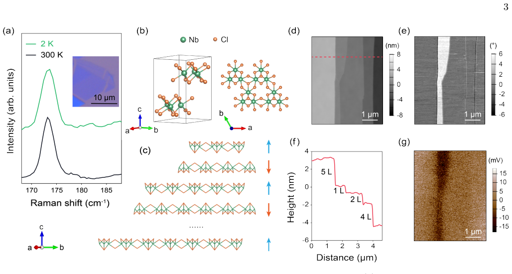
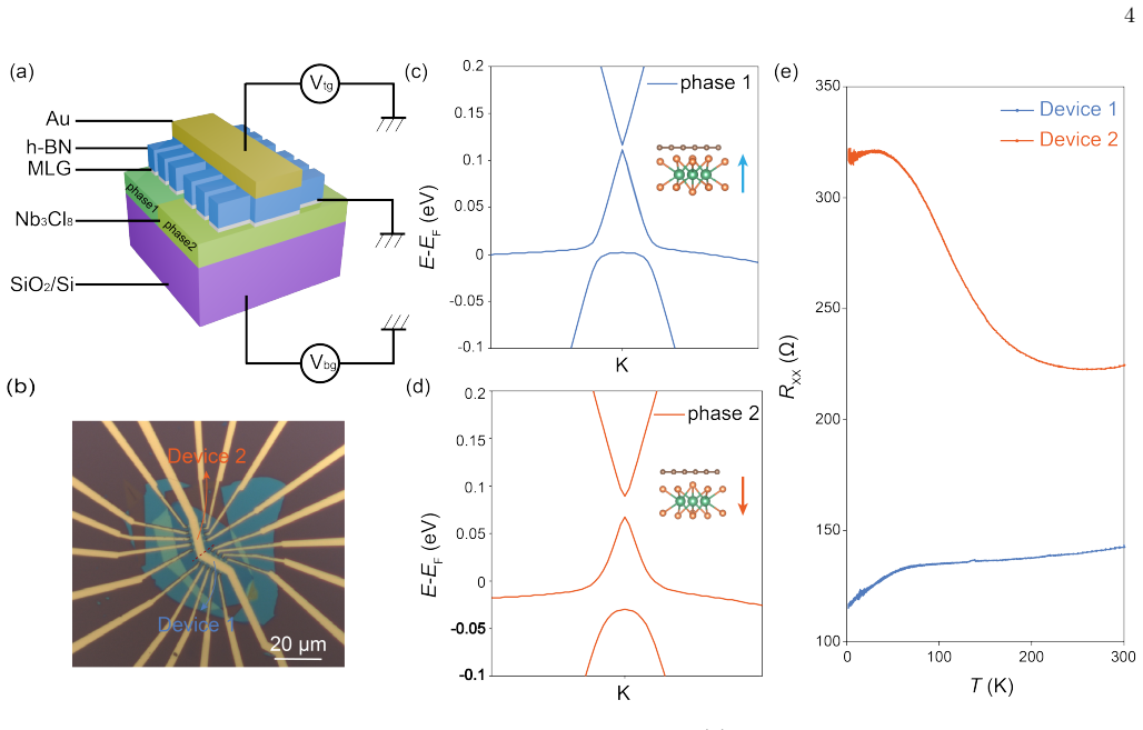
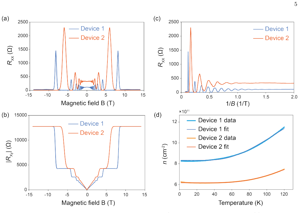
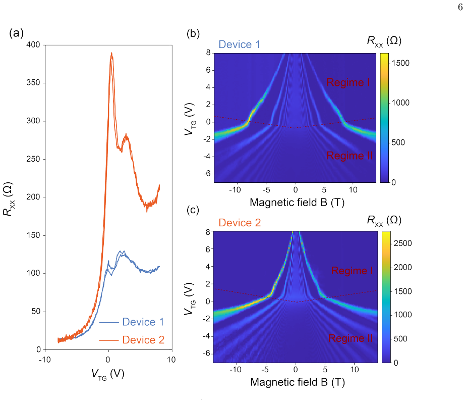
Nb3Cl8, a single-band Mott insulator, shows an out-of-plane polarization in its topmost layer that oscillates with layer parity. When distinct surface phases of Nb3Cl8 are placed in contact with graphene, the parity-dependent polarizations produce different interfacial orbital overlaps, resulting in phase-specific charge transfer, carrier densities, and hybridization gaps of 25.2 meV (Phase 1) and 30.0 meV (Phase 2).
What carries the argument
Layer-parity-dependent out-of-plane polarization of the topmost Nb3Cl8 layer, which controls orbital overlap and coupling strength at the van der Waals interface.
If this is right
- Interface properties in strongly correlated vdW stacks can be selected by choosing the parity of the topmost layer.
- Hybridization gap and charge transfer become discrete, parity-tunable quantities rather than continuously variable parameters.
- Orbital orientation at the interface becomes a controllable degree of freedom for engineering carrier density and gap size.
- Surface polarization mapping with KPFM can serve as a non-destructive proxy for predicting transport behavior before device fabrication.
Where Pith is reading between the lines
- Similar parity-dependent polarization effects may appear in other layered Mott insulators and could be used to create parity-selective contacts.
- The observed gap difference suggests that parity engineering might extend to controlling proximity-induced magnetism or superconductivity at the interface.
- Device designs could incorporate local parity selection via thickness patterning to create regions with different coupling strengths on the same flake.
Load-bearing premise
The two surface phases identified by AFM and KPFM correspond to different layer parities and their polarization directly produces the observed differences in interfacial coupling.
What would settle it
Transport measurements on devices where the Nb3Cl8 surface phase is fixed while layer parity is varied independently, or where polarization is measured to be identical across phases, would show no difference in hybridization gap or carrier density.
Figures
read the original abstract
Strongly correlated two-dimensional systems provide compelling platforms for investigating exotic quantum phenomena. Niobium chloride (Nb$_3$Cl$_8$), a single-band Mott insulator, exhibits a remarkable out-of-plane polarization in its topmost layer that oscillates with layer parity, manifesting as an odd-even effect. Using atomic force microscopy (AFM) and Kelvin probe force microscopy (KPFM), this layer-parity-dependent polarization can be effectively characterized through surface morphology and potential mapping, enabling the unambiguous identification of different surface phases. We then fabricated dual-gate Hall devices by coupling different surface phases of Nb$_3$Cl$_8$ with monolayer graphene to investigate how the topmost-layer out-of-plane polarization influences interfacial coupling and the resulting transport behavior. Our results reveal significant phase-dependent variations in charge transfer, carrier densities, and hybridization gaps (25.2 meV for Phase 1 and 30.0 meV for Phase 2). Density functional theory calculations corroborate these experimental findings, showing that distinct out-of-plane polarizations in the topmost layer lead to different orbital overlaps and interfacial coupling strengths. These findings highlight the critical importance of surface polarization and orbital orientation in engineering the properties of strongly correlated van der Waals heterostructures.
Editorial analysis
A structured set of objections, weighed in public.
Referee Report
Summary. The paper claims that Nb3Cl8 exhibits layer-parity-dependent out-of-plane polarization in its topmost layer, which can be identified via AFM morphology and KPFM potential maps as distinct surface phases. Coupling these phases to monolayer graphene in dual-gate Hall devices produces measurable differences in charge transfer, carrier densities, and hybridization gaps (25.2 meV for Phase 1 vs. 30.0 meV for Phase 2). DFT calculations are presented as corroborating that the polarization differences drive distinct orbital overlaps and interfacial coupling strengths.
Significance. If the phase-to-parity assignment is validated, the result would demonstrate a concrete route to parity-controlled interfacial hybridization in a Mott-insulating vdW system, with direct relevance to engineering correlated heterostructures. The reported gap values and DFT orbital-overlap analysis constitute falsifiable, quantitative predictions that could be tested independently.
major comments (2)
- [Abstract and results section describing phase assignment] The central claim that the two AFM/KPFM-identified phases correspond to odd vs. even layer parity (and that this parity difference, rather than thickness, defects, or chemistry, produces the 25.2 meV vs. 30.0 meV gap difference) is load-bearing yet rests on an unverified mapping. AFM/KPFM measure integrated topography and electrostatics; they do not directly resolve layer count or stacking sequence. No cross-sectional TEM, electron diffraction, or other atomic-scale confirmation is referenced to close this loop, leaving the polarization-to-coupling causal link as an assumption.
- [Abstract / Transport results] The abstract states measured gap values and DFT support but supplies no error bars, number of devices or samples per phase, or explicit criteria used to assign phases to parities. Without these statistics the reported 4.8 meV difference cannot be assessed for significance or reproducibility.
minor comments (2)
- The abstract refers to 'dual-gate Hall devices' without specifying gate dielectric, channel dimensions, or measurement temperature; these details are needed to interpret the carrier-density and gap extractions.
- Notation for the two phases (Phase 1/Phase 2) should be tied explicitly to odd/even parity throughout the text and figures for clarity.
Simulated Author's Rebuttal
We thank the referee for the detailed and constructive report. We address the two major comments point by point below, indicating where revisions will be made to strengthen the manuscript.
read point-by-point responses
-
Referee: [Abstract and results section describing phase assignment] The central claim that the two AFM/KPFM-identified phases correspond to odd vs. even layer parity (and that this parity difference, rather than thickness, defects, or chemistry, produces the 25.2 meV vs. 30.0 meV gap difference) is load-bearing yet rests on an unverified mapping. AFM/KPFM measure integrated topography and electrostatics; they do not directly resolve layer count or stacking sequence. No cross-sectional TEM, electron diffraction, or other atomic-scale confirmation is referenced to close this loop, leaving the polarization-to-coupling causal link as an assumption.
Authors: We agree that AFM/KPFM provide integrated rather than atomically resolved data and that direct confirmation via cross-sectional TEM or electron diffraction would strengthen the parity assignment. The phase identification in the manuscript relies on the established odd-even polarization oscillation in Nb3Cl8 (previously reported in the literature) combined with distinct KPFM potential maps and AFM morphologies that match the expected polarization contrast. DFT calculations then link these polarization differences to the observed orbital overlaps and gap values. We will revise the results section to explicitly state the inference steps, add a dedicated paragraph discussing the limitations of the AFM/KPFM mapping, and note that future atomic-scale validation would be valuable. The causal connection to interfacial coupling remains supported by the quantitative match between experiment and DFT. revision: partial
-
Referee: [Abstract / Transport results] The abstract states measured gap values and DFT support but supplies no error bars, number of devices or samples per phase, or explicit criteria used to assign phases to parities. Without these statistics the reported 4.8 meV difference cannot be assessed for significance or reproducibility.
Authors: The referee is correct that the abstract omits these details. The full results section contains the device statistics (multiple devices per phase), the KPFM potential threshold criteria used for phase assignment, and the measured gap values with standard deviations. We will revise the abstract to include error bars on the reported gaps, the number of devices and samples measured for each phase, and a concise statement of the assignment criteria. This will allow readers to evaluate the 4.8 meV difference directly. revision: yes
Circularity Check
No significant circularity; central results are direct experimental measurements corroborated by standard DFT
full rationale
The paper reports AFM/KPFM surface characterization, dual-gate Hall transport data yielding charge transfer and hybridization gaps (25.2 meV vs 30.0 meV), and separate DFT calculations. No equations or derivations reduce the reported gaps or coupling strengths to parameters fitted from the same dataset. The phase-to-parity mapping is an interpretive assumption, but it does not constitute a self-definitional loop or fitted-input prediction. Standard external DFT and experimental benchmarks keep the work self-contained; any self-citation is not load-bearing for the measured quantities.
Axiom & Free-Parameter Ledger
axioms (2)
- domain assumption Surface phases mapped by AFM/KPFM correspond to odd versus even layer parity
- standard math Density functional theory accurately captures orbital overlap at the Nb3Cl8/graphene interface
Reference graph
Works this paper leans on
-
[1]
The electron orbital distributions visualized how these different surface terminations affect the spa- tial extent and orientation of the Nbd-orbitals at the interface (Fig
or more exposed Nb 3 cluster (downward polarization, Phase 2). The electron orbital distributions visualized how these different surface terminations affect the spa- tial extent and orientation of the Nbd-orbitals at the interface (Fig. S2). Considering that the role of Cl is to form chemical bonds and fix Nb in the triangular cluster, thereby maintaining...
-
[2]
T.et al.Emergence of high-temperature su- perconductivity at the interface of two mott insulators
Ju L, R. T.et al.Emergence of high-temperature su- perconductivity at the interface of two mott insulators. Physical Review B2, 105 (2022)
2022
-
[3]
L.et al.Origin of mott insulating behavior and superconductivity in twisted bilayer graphene.Phys- ical Review X3, 8 (2018)
Po H C, Z. L.et al.Origin of mott insulating behavior and superconductivity in twisted bilayer graphene.Phys- ical Review X3, 8 (2018)
2018
-
[4]
D.et al.Field-induced kitaev multipolar liquid in spin-orbit coupled d 2 honeycomb mott insula- tors.Physical Review B2, 107 (2023)
Rayyan A, C. D.et al.Field-induced kitaev multipolar liquid in spin-orbit coupled d 2 honeycomb mott insula- tors.Physical Review B2, 107 (2023)
2023
-
[5]
S.et al.Thermal and magnetoelastic properties ofα-rucl 3 in the field-induced low-temperature states.Physical Review B21, 102 (2020)
Sch¨ onemann R, I. S.et al.Thermal and magnetoelastic properties ofα-rucl 3 in the field-induced low-temperature states.Physical Review B21, 102 (2020)
2020
-
[6]
Xiang, Z.et al.Imaging quantum melting in a disordered 2d wigner solid.Physical Review B388, 736–740 (2025). 9
2025
-
[7]
Kumar A, H. N. C.et al.Gate-tunable heavy fermion quantum criticality in a moir´ e kondo lattice.Physical Review B4, 106 (2022)
2022
-
[8]
Li, W.et al.Signatures of fractional charges via anyon–trions in twisted mote 2.Nature651, 48–53 (2026)
2026
-
[9]
Lu, H., Z.et al.Fractional quantum anomalous hall effect in multilayer graphene.Nature626, 759–764 (2024)
2024
-
[10]
Gao, S.et al.Discovery of a single-band mott insulator in a van der waals flat-band compound.Physical Review X13, 041049 (2023)
2023
-
[11]
H.et al.Observation of topological flat bands in the kagome semiconductor nb 3cl8.Nano Letters11, 4596–4602 (2022)
Sun Z, Z. H.et al.Observation of topological flat bands in the kagome semiconductor nb 3cl8.Nano Letters11, 4596–4602 (2022)
2022
-
[12]
M.et al.Evidence of mott insulator with thermally induced melting behavior in kagome compound nb3cl8.National Science Review12, 4 (2025)
Yang Q, W. M.et al.Evidence of mott insulator with thermally induced melting behavior in kagome compound nb3cl8.National Science Review12, 4 (2025)
2025
-
[13]
arXiv preprint arXiv2506, 21837 (2025)
Gao, Z.et al.Designer heavy fermions in incommen- surate Nb3Cl8/graphene van der waals heterostructures. arXiv preprint arXiv2506, 21837 (2025)
2025
-
[14]
Vanˇo, V.et al.Artificial heavy fermions in a van der waals heterostructure.Nature599, 582–586 (2021)
2021
-
[15]
L.et al.Proximity-induced charge density wave in a metallic system.Physical Review B11, 107 (2023)
Banerjee A, H. L.et al.Proximity-induced charge density wave in a metallic system.Physical Review B11, 107 (2023)
2023
-
[16]
Y.et al.Suppression of structural and mag- netic phase transitions in layered exfoliated kagome semi- conductor Nb3Cl8.Newton2950–6360 (2025)
Huang X, Z. Y.et al.Suppression of structural and mag- netic phase transitions in layered exfoliated kagome semi- conductor Nb3Cl8.Newton2950–6360 (2025)
2025
-
[17]
Huang, X.et al.Layer-parity-defined surface polariza- tion in nb 3cl8 for excitonic modulation at van der waals interfaces.arXiv preprint arXiv2606, 09277 (2026)
2026
-
[18]
Sheckelton J P, P. K. W.et al.Rearrangement of van der waals stacking and formation of a singlet state at t=90 k in a cluster magnet.Inorganic Chemistry Frontiers3, 481–490 (2017)
2017
-
[19]
Haraguchi Y, Y. K.et al.Molecular orbital electronic instability in the van der waals kagom´ e semiconductor Nb3Cl8: Exploring future directions.Journal of the Physical Society of Japan11, 93 (2024)
2024
-
[20]
H.et al.Observation of topological flat bands in the kagome semiconductor Nb 3Cl8.Nano Letters11, 4596–4602 (2022)
Sun Z, Z. H.et al.Observation of topological flat bands in the kagome semiconductor Nb 3Cl8.Nano Letters11, 4596–4602 (2022)
2022
-
[21]
Grytsiuk, S.et al.Nb 3Cl8: a prototypical layered mott- hubbard insulator.npj Quantum Materials9, 8 (2024)
2024
-
[22]
E.et al.Anomalous thickness-dependent elec- trical conductivity in van der waals layered transition metal halide, Nb 3Cl8.Journal of Physics: Condensed Matter30, 32 (2020)
Yoon J, L. E.et al.Anomalous thickness-dependent elec- trical conductivity in van der waals layered transition metal halide, Nb 3Cl8.Journal of Physics: Condensed Matter30, 32 (2020)
2020
-
[23]
R.et al.Standardization of surface poten- tial measurements of graphene domains.Scientific Re- ports1, 3 (2013)
Panchal V, P. R.et al.Standardization of surface poten- tial measurements of graphene domains.Scientific Re- ports1, 3 (2013)
2013
-
[24]
X.et al.Interlayer charge transfer induced by electronic instabilities in the natural van der waals heterostructure 4 h b-tas2.Physical Review Letters 11, 135 (2025)
Mathew Roy R, F. X.et al.Interlayer charge transfer induced by electronic instabilities in the natural van der waals heterostructure 4 h b-tas2.Physical Review Letters 11, 135 (2025)
2025
-
[25]
W.et al.Direct evidence of intrinsic mott state and its layer-parity oscillation in a breathing kagome crystal down to monolayer.Physical Review Letters7, 135 (2025)
Liu H, L. W.et al.Direct evidence of intrinsic mott state and its layer-parity oscillation in a breathing kagome crystal down to monolayer.Physical Review Letters7, 135 (2025)
2025
-
[26]
Liang, Y.et al.A universal model for accurately predict- ing the formation energy of inorganic compounds.Sci- ence China Materials66, 343–351 (2022)
2022
-
[27]
Tilak, N.et al.Proximity-induced charge density wave in a graphene/1t-tas 2 heterostructure.Nature Commu- nications15, 8056 (2024)
2024
-
[28]
Huhtasaari J, P. J. J.et al.Wafer-scale single-crystalline monolayer graphene.arXiv preprint arXiv2512, 00394 (2025)
2025
-
[29]
Sucharitakul S, K. U. R.et al.Screening limited switch- ing performance of multilayer 2d semiconductor fets: the case for sns.Nanoscale45, 8 (2016)
2016
-
[30]
Wang, Y.et al.Quantum hall phase in graphene engi- neered by interfacial charge coupling.Nature Nanotech- nology17, 1272–1279 (2022)
2022
-
[31]
Yang, K.et al.Unconventional correlated insulator in croclinterfaced bernal bilayer graphene.Nature Commu- nications14, 2136 (2023)
2023
-
[32]
A.et al.Shubnikov–de haas oscillations reaching the quantum limit in two-dimensional electron systems at srtio 3 (111) interfaces.Physical Review B3, 112 (2025)
Wang Z, H. A.et al.Shubnikov–de haas oscillations reaching the quantum limit in two-dimensional electron systems at srtio 3 (111) interfaces.Physical Review B3, 112 (2025)
2025
-
[33]
B.et al.Quantum espresso: a modu- lar and open-source software project for quantum simula- tions of materials.Journal of Physics: Condensed Matter 21, 395502 (2009)
Paolo Giannozzi, S. B.et al.Quantum espresso: a modu- lar and open-source software project for quantum simula- tions of materials.Journal of Physics: Condensed Matter 21, 395502 (2009)
2009
-
[34]
A.et al.Advanced capabilities for materials modelling with quantum espresso.Journal of Physics: Condensed Matter29, 465901 (2017)
P Giannozzi, O. A.et al.Advanced capabilities for materials modelling with quantum espresso.Journal of Physics: Condensed Matter29, 465901 (2017)
2017
discussion (0)
Sign in with ORCID, Apple, or X to comment. Anyone can read and Pith papers without signing in.