REVIEW 3 major objections 5 minor 83 references
Movable Dirac Points with Ferroelectrics: Kink States and Berry Curvature Dipoles
T0 review · 3 major / 5 minor · reviewed 2026-08-07 · deepseek-v4-flash
Pith's one-line read Moving Dirac points flips kink-state conductance and SHG.
desk verdict The tight-binding core is clean and the kink-state/Dirac-fusion predictions are worth taking seriously; the Cl2Rh2S2-GeS material claim outruns the evidence until the TB parameters are extracted from DFT. read the letter →
The pith
A machine-rendered reading of the paper's core claim, the machinery that carries it, and where it could break.
The reading
What carries the argument
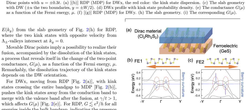
The central object is a two-chain tight-binding model of coupled zigzag chains, each with two inequivalent sublattices, with nearest-neighbor hopping $t$, inter-chain coupling $\gamma$, and a staggered on-site potential $V = u\,\sigma_z\tau_z$ that breaks inversion and models the ferroelectric polarization. The gapless Dirac points sit at positions set by $\cos(k_D^\pm a_0/2) = \gamma/t$, so the ratio $\gamma/t$ moves the points from remote ($\gamma/t \lesssim 0.8$) toward merged ($\gamma/t \to 1$); the potential $u$ opens a gap and generates Berry curvature $\Omega_k = (u t^2/16E^3)\, a_0 b_0 \sin(k_x a_0)$. Domain walls where the sign of $u$ flips host topological kink states whose dispersion and conductance are computed with a quantum transport code, and the same model's Berry curvature dipole enters the second-harmonic Hall conductivity through $\chi^H_{2\omega} \propto \int dk\, \partial\Omega^{cv}_k/\partial k_x\, \Theta(2\omega - \omega_{cv})$. The model is anchored to a real system by first-principles calculations for a Cl$_2$Rh$_2$S$_2$–GeS junction, where strain is shown to move the Dirac points and the FE polarization to open gaps of 33.3 meV and 18.0 meV with opposite Berry curvature.
What would settle it
Apply uniaxial strain to a Cl$_2$Rh$_2$S$_2$–GeS junction while measuring the two-terminal conductance across a single ferroelectric domain wall: if the conductance inside the gap does not show the predicted drop from about $e^2/h$ (remote points) to about $0$ (merged points) as the Dirac points are driven together, the mapping of the domain wall to a sign-flip staggered potential is wrong. Alternatively, a second-harmonic measurement that shows no peak in $|\chi^H_{2\omega}|$ as the Dirac points fuse at $\gamma \approx t$ would invalidate the Berry-curvature-dipole switching mechanism.
Extended reading notes
Core claim
The central claim is that movable Dirac points, gapped by an in-plane ferroelectric polarization, act as the controlling ingredient for both topological kink-state transport and nonlinear optical response. For domain walls parallel to $x$, the kink states evolve from spanning the whole bandgap at remote Dirac points ($\gamma/t \lesssim 0.8$) to merging with the valence band after the Dirac points fuse at the $\Gamma$-point ($\gamma/t > 1$), so that the two-terminal conductance $G(\mu)$ drops from about $e^2/h$ to zero near the gap center; for domain walls parallel to $y$, the two counterpropagating kink states open a gap and split, leaving $G = 0$ in the middle of the gap. The Berry curvature dipole, which controls the second-harmonic Hall conductivity, shows a peak in $|\chi^H_{2\omega}|$ at the fusion point $\gamma \approx t$ and an enhanced region for well-separated remote Dirac points at small $\gamma$, giving a zero-to-nonzero switch of the SHG signal as the Dirac point position is tuned. These predictions are supported by tight-binding transport calculations and by first-principles results showing gapped Dirac points with opposite Berry curvature in the two ferroelectric states of a Cl$_2$Rh$_2$S$_2$–GeS junction.
Load-bearing premise
The load-bearing assumption is that the ferroelectric substrate's only effect on the Dirac material is a local staggered potential that opens a gap, while leaving the hopping parameters $t$ and $\gamma$—and therefore the Dirac point positions—unchanged; if the real interface also modifies $\gamma/t$ through strain or proximity, the remote-to-merged crossover on which the predicted conductance and SHG switching depend would happen at a different material condition.
Editorial extensions
If this is right
- At remote Dirac points, a domain wall along $x$ hosts a single ballistic kink channel with $G \approx e^2/h$ across the gap; merging the points ($\gamma/t > 1$) removes the channel and drives $G \to 0$ near the gap center.
- For domain walls along $y$, merging the Dirac points opens a gap between the two counterpropagating kink states, leaving $G = 0$ in the middle of the bandgap.
- The second-harmonic Hall conductivity $|\chi^H_{2\omega}|$ switches from a near-zero value for well-separated remote Dirac points to a peak at the fusion point $\gamma \approx t$, providing an optical signature of the Dirac point merger.
- First-principles calculations for a Cl$_2$Rh$_2$S$_2$–GeS junction show gapped Dirac points with opposite Berry curvature in the two ferroelectric states (gaps of 33.3 meV and 18.0 meV), and strain-driven fusion of the Dirac points under $-2.5$% deformation, mapping $\gamma/t$ from 0.7 through 1 to 1.2.
- The tunable gap of movable Dirac points permits pumping charges between bulk and kink states without closing the gap, and the analysis extends to 2D magnets with a single pair of Weyl points and to Dirac points at generic positions in the Brillouin zone.
Reading between the lines
- A quantitative next step would be to extract the tight-binding parameters $t$ and $\gamma$ directly from the first-principles band structure of the Cl$_2$Rh$_2$S$_2$–GeS junction; that would map the predicted remote-to-merged crossover to a specific strain or polarization condition, turning the conductance drop into an experimentally schedulable event.
- Because the kink-state conductance distinguishes the two domain-wall orientations, a multi-terminal device with both DW$_x$ and DW$_y$ segments would read out which Dirac regime the material is in from a single sample.
- The SHG peak at the fusion point could be used as a contact-free probe of Dirac point merger, and the same Berry-curvature-dipole rectification should appear in other systems with gapped, movable two-band crossings, such as gapped Weyl points in 2D magnets.
Editorial analysis
A structured set of objections, weighed in public.
Referee Report
Summary. The manuscript studies a four-band tight-binding model of two coupled zigzag chains whose band structure hosts movable Dirac points. A chain-dependent staggered potential u, attributed to an in-plane ferroelectric polarization, gaps the Dirac points and yields topological kink states at structural domain walls. The authors show that, as the interchain coupling γ/t evolves from remote Dirac points (RDP) to merged Dirac points (MDP), the kink-state dispersion and the two-terminal conductance G(μ) change in a domain-wall-orientation-dependent manner, and that the interband Berry curvature dipole switches the subgap second-harmonic Hall conductivity χ_H^{2ω}. They support the proposed platform with first-principles calculations for a Cl2Rh2S2-GeS junction, reporting polarization-dependent gaps and opposite Berry curvature, and they list 36 candidate materials in the Supplemental Material.
Significance. If the full chain of arguments is established, the paper would identify a new control knob, the position and fusion of Dirac points, for topological edge-channel transport and nonlinear optical response. The analytic tight-binding results are clear, internally consistent, and presented with explicit formulas for the spectrum, Berry curvature, and SHG response. The material screening and the first-principles results add useful concrete context. The main limitation is that the connection between the model and the specific ferroelectric/Dirac-material junction is asserted rather than demonstrated; the central predictions are presently properties of the tight-binding family unless effective parameters are extracted from the first-principles calculations. No code or data availability statement is provided, but the transport calculation uses the standard Kwant package and the analytic formulas are given in the text.
major comments (3)
- [Eq. (3), Fig. 3, and the paragraph introducing electro-elastic coupling] The model-to-material mapping is the load-bearing step. The paper assumes that the ferroelectric proximity effect is fully captured by a local staggered potential u σ_z τ_z, that t and γ are unchanged, and that a domain wall is simply a sign flip of u. No effective tight-binding parameters are extracted from the first-principles bands of the Cl2Rh2S2-GeS junction; the DFT panels report only zero-field gaps (33.3 and 18.0 meV) and Berry curvature. The manuscript itself notes that electro-elastic coupling changes TB parameters, and its own strain calculations move γ/t from 0.7 at +5% deformation to 1 at −2.5% and to 1.2 at −5%. Ferroelectric switching in the actual junction may therefore change γ/t together with u, and the RDP/MDP crossover on which the conductance and SHG signatures rest is not guaranteed. I ask the authors to either fit t, γ, and u for the FE1 and FE2 states and show whether the RDP/MDP crossover occurs in the junction, or explicitly delimit the transport and SHG predictions as model results that are not yet tied to the Cl2Rh2S2-GeS device.
- [Fig. 3 and the paragraph on deformed pristine Cl2Rh2S2] The DFT evidence does not directly establish movable Dirac points in the proposed junction. The strain-dependent calculations are performed on pristine monolayer Cl2Rh2S2, not on the Cl2Rh2S2-GeS heterostructure, and the FE1/FE2 band structures are shown only after the gap has opened. It is therefore not demonstrated that ferroelectric switching moves the Dirac points in the actual device; it is demonstrated that the two FE states have different gaps and opposite Berry curvature. The parameter evolution used for the conductance and SHG predictions should be tied to the junction calculations, or the claims should be explicitly scoped to the model.
- [Fig. 1(b) and Fig. 3(a)-(d)] The orientation correspondence between the model and the material is not stated. The tight-binding model places the Dirac points along Γ–X and defines DWx and DWy relative to that axis, while the DFT calculation for Cl2Rh2S2 reports paired Dirac points along Γ–Y. Since the central transport claim is that kink-state conductance is sensitive to the crystallographic orientation of the domain walls, the relation between the model axes and the material axes should be explained explicitly; otherwise the material-specific orientation dependence is not tested.
minor comments (5)
- [Fig. 3 caption] The caption jumps from panel (a) to panels (c) and (d) with no panel (b), and the text refers to Figs. 3(b) and 3(c) while the caption uses (c) and (d); the labels should be made consistent.
- [Fig. 1 caption] There is a typo, 'Brilluion zone', which should read 'Brillouin zone'.
- [Fig. 4 caption and main text] The caption uses δℏω while the main text uses δω for the subgap detuning; the notation should be unified.
- [Final paragraph] The word 'trough' should be 'through' in the sentence about tunable proximity effects.
- [Data and code availability] The paper provides no statement about availability of the first-principles parameters, tight-binding transport scripts, or SHG calculation code, which would help reproducibility of the quantitative results.
Circularity Check
No significant circularity: the model predictions are derived from an explicit tight-binding Hamiltonian, with first-principles calculations serving as an external check.
full rationale
The central derivation chain begins from the explicit tight-binding Hamiltonian H = H0 + V in Eqs. (1)-(3), with parameters t, gamma, and u. From this Hamiltonian the paper derives the Dirac point positions, the Berry curvature in Eq. (4), the kink-state spectra in Fig. 2, the conductance G(mu) computed with Kwant, and the second-harmonic Hall conductivity from Eq. (5). None of these predicted outputs is used to define or fit the input parameters: gamma/t and u are scanned as model parameters, and the transport and SHG results are functions of those parameters, not fits to them. The first-principles Cl2Rh2S2-GeS calculations provide an external check by reporting a band gap and Berry curvature for the FE1/FE2 states and by showing strain-induced motion of the Dirac points, but no transport or SHG prediction is fitted to those DFT data. The strain results are translated into gamma/t values, but this is a comparison between the model and a material realization, not a construction that forces the predicted conductance or SHG. The self-citations (refs. 13, 21, 49, 83) are used for context, for the general statement about suppressing disorder-induced scattering, or for proximity-effect background; they do not supply a uniqueness theorem or define the central quantities, so they are not load-bearing in a circular way. The FE-to-model mapping, which assumes the ferroelectric proximity effect is a local staggered potential that leaves t and gamma unchanged, is a modeling assumption and a validation gap, but it is not a circular reduction: the model's predictions are logically independent of whether that mapping is quantitatively accurate for a specific heterostructure. Therefore no specific circular step can be exhibited, and the paper's derivations are self-contained relative to their stated model assumptions.
Assumptions & free parameters
free parameters (4)
- interchain coupling γ/t =
0.6 (remote), 0.95 (merged), 1.2 (trivial); mapped from +5%, -2.5%, -5% strain in Cl2Rh2S2
- staggered potential u =
0.3t in Fig. 2 (u=±0.3t)
- Fermi energy μ =
varied across the gap
- SHG detuning δω = 2ω - ω_cv =
0.1u, 0.2u, 0.3u
assumptions (4)
- standard math Berry-phase/Kubo formalism for Berry curvature and nonlinear conductivity (Eqs. 4-5).
- standard math Volkov-Pankratov/index theorem guarantees kink states at mass domain walls.
- domain assumption DFT approximations used in the Supplemental Material accurately describe Cl2Rh2S2-GeS and the strain dependence of Cl2Rh2S2.
- ad hoc to paper The ferroelectric polarization acts as a local staggered potential u without altering the hopping parameters t and γ.
Cite this review
Pith. "Pith review of Movable Dirac Points with Ferroelectrics: Kink States and Berry Curvature Dipoles." pith.science (2026). https://pith.science/paper/J7SL67SG
@misc{pith2026250613960,
  author       = {Pith},
  title        = {Pith review of: Movable Dirac Points with Ferroelectrics: Kink States and Berry Curvature Dipoles},
  year         = {2026},
  howpublished = {\url{https://pith.science/paper/J7SL67SG}},
  note         = {Machine review of arXiv:2506.13960}
}
abstract
Two-dimensional (2D) Dirac states and Dirac points with linear dispersion are the hallmark of graphene, topological insulators, semimetals, and superconductors. Lowering a symmetry by the ferroelectric polarization opens the gap in Dirac points and introduces finite Berry curvature. Combining this with Dirac points detached from high symmetry points of the Brillouin zone offers additional ways to tailor topological properties. We explore this concept by studying topological phenomena emerging in 2D materials with movable Dirac points and broken out-of-plane mirror reflection. The resulting topological kink states and Berry curvature dipoles are changed by movable 2D Dirac points with experimental signatures in electrical conductance and second-harmonic nonlinear Hall conductivity. We identify materials platforms where our predictions can be realized and support that with the first-principles results for Cl$_2$Rh$_2$S$_2$-GeS junction.
Figures


Figures from the paper (1 more)

Reference graph
Works this paper leans on
-
[1]
Next generation ferroelectric materials for semiconductor process integration and their applica- tions,
T. Mikolajick, S. Slesazeck, H. Mulaosmanovic, M. H. Park, S. Fichtner, P. D. Lomenzo, M. Hoffmann, and U. Schroeder, “Next generation ferroelectric materials for semiconductor process integration and their applica- tions,” J. Appl. Phys. 129, 100901 (2021)
2021
-
[2]
Electrostatic modi- fication of novel materials,
C. H. Ahn, A. Bhattacharya, M. Di Ventra, J. N. Eck- stein, C. D. Frisbie, M. E. Gershenson, A. M. Goldman, I. H. Inoue, J. Mannhart, A. J. Millis, A. F. Morpurgo, D. Natelson, and J.-M. Triscone, “Electrostatic modi- fication of novel materials,” Rev. Mod. Phys. 78, 1185 (2006)
2006
-
[3]
Twist-resilient and ro- bust ferroelectric quantum spin Hall insulators driven by van der Waals interactions,
A. Marrazzo and M. Gibertini, “Twist-resilient and ro- bust ferroelectric quantum spin Hall insulators driven by van der Waals interactions,” npj 2D Mater. Appl. 6, 30 (2022)
2022
-
[4]
Two-dimensional multiferroics in monolayer group IV monochalcogenides,
H. Wang and X. Qian, “Two-dimensional multiferroics in monolayer group IV monochalcogenides,” 2D Mater. 4, 015042 (2017)
work page 2017
-
[5]
Heterobilayer with Ferroelectric Switching of Topological State,
J.-J Zhang, D. Zhu, and B. I. Yakobson, “Heterobilayer with Ferroelectric Switching of Topological State,” Nano Lett. 21, 785 (2020)
work page 2020
-
[6]
Ferroelectric Control of Magnetic Skyrmions in Two-Dimensional van der Waals Heterostructures,
K. Huang, D.-F. Shao, and E. Y. Tsymbal, “Ferroelectric Control of Magnetic Skyrmions in Two-Dimensional van der Waals Heterostructures,” Nano Lett.22, 3349 (2022)
work page 2022
-
[7]
Weyl and Dirac semimetals in three-dimensional solids,
N. P. Armitage, E. J. Mele, and A. Vishwanath, “Weyl and Dirac semimetals in three-dimensional solids,” Rev. Mod. Phys. 90, 015001 (2018)
work page 2018
-
[8]
X. Wan, A. M. Turner, A. Vishwanath, and S. Y. Savrasov, “Topological semimetal and Fermi-arc surface states in the electronic structure of pyrochlore iridates,” Phys. Rev. B 83, 205101 (2011)
work page 2011
Show all 83 references
-
[9]
Dirac Semimetals in Two Dimensions,
S. M. Young and C. L. Kane, “Dirac Semimetals in Two Dimensions,” Phys. Rev. Lett. 115, 126803 (2015)
2015
-
[10]
Two-Dimensional Dirac Semimetals with- out Inversion Symmetry,
Y. J. Jin, B. B. Zheng, X. L. Xiao, Z. J. Chen, Y. Xu, and H. Xu, “Two-Dimensional Dirac Semimetals with- out Inversion Symmetry,” Phys. Rev. Lett. 125, 116402 (2020)
2020
-
[11]
Wallpaper fermions and the nonsymmorphic Dirac insulator,
B. J Wieder, B. Bradlyn, Z. Wang, J. Cano, Y. Kim, H.-S. D. Kim, A. M. Rappe, C. L. Kane, and B. A. Bernevig, “Wallpaper fermions and the nonsymmorphic Dirac insulator,” Science 361, 246 (2018)
2018
-
[12]
Tunable Dirac points in a two-dimensional non-symmorphic wallpaper group lattice,
M. A. J. Herrera and D. Bercioux, “Tunable Dirac points in a two-dimensional non-symmorphic wallpaper group lattice,” Commun. Phys. 6, 42 (2023)
2023
-
[13]
Vacancy- enginered nodal-line semimetals,
F. Liu, F. Qu, I. ˇZuti´ c, and M. Malard, “Vacancy- enginered nodal-line semimetals,” Sci. Rep. 12, 14981 (2022)
2022
-
[14]
Vanderbilt, Berry Phases in Electronic Structure The- ory (Cambridge University Press, Cambridge, 2018)
D. Vanderbilt, Berry Phases in Electronic Structure The- ory (Cambridge University Press, Cambridge, 2018)
2018
-
[15]
Berry phase ef- fects on electronic properties,
D. Xiao, M.-C. Chang, and Q. Niu, “Berry phase ef- fects on electronic properties,” Rev. Mod. Phys. 82, 1959 (2010)
2010
-
[16]
Quantum Spin Hall Effect in Graphene,
C. L. Kane and E. J. Mele, “Quantum Spin Hall Effect in Graphene,” Phys. Rev. Lett. 95, 226801 (2005)
2005
-
[17]
Z2 Topological Order and the Quantum Spin Hall Effect,
C. L. Kane and E. J. Mele, “Z2 Topological Order and the Quantum Spin Hall Effect,” Phys. Rev. Lett. 95, 146802 (2005)
2005
-
[18]
Topolog- ical Confinement in Bilayer Graphene,
I. Martin, Y. M. Blanter, and A. F. Morpurgo, “Topolog- ical Confinement in Bilayer Graphene,” Phys. Rev. Lett. 100, 036804 (2008)
2008
-
[19]
Do- main Walls in Gapped Graphene,
G. W. Semenoff, V. Semenoff, and F. Zhou, “Do- main Walls in Gapped Graphene,” Phys. Rev. Lett. 101, 087204 (2008)
2008
-
[20]
Valley-Hall kink and edge states in multilayer graphene,
J. Jung, F. Zhang, Z. Qiao, and A. H. MacDon- ald, “Valley-Hall kink and edge states in multilayer graphene,” Phys. Rev. B 84, 075418 (2011)
2011
-
[21]
Quantum Spin-Valley Hall Kink States: From Concept to Materials Design,
T. Zhou, S. Cheng, M. Schleenvoigt, P. Sch¨ uffelgen, H. Jiang, Z. Yang, and I. ˇZuti´ c, “Quantum Spin-Valley Hall Kink States: From Concept to Materials Design,” Phys. Rev. Lett. 127, 116402 (2021)
2021
-
[22]
Topological val- ley transport at bilayer graphene domain walls,
L. Ju, Z. Shi, N. Nair, Y. Lv, C. Jin, J. Velasco Jr., C. Ojeda-Aristizabal, H. A. Bechtel, M. C. Martin, A. Zettl, J. Analytis, and F. Wang, “Topological val- ley transport at bilayer graphene domain walls,” Nature 520, 650 (2015)
2015
-
[23]
A valley valve and electron beam splitter,
J. Li, R.-X. Zhang, Z. Yin, J. Zhang, K. Watanabe, T. Taniguchi, C. Liu, and J. Zhu, “A valley valve and electron beam splitter,” Science 362, 1149 (2018)
2018
-
[24]
High-temperature quantum valley Hall effect with quantized resistance and a topological switch,
K. Huang, H. Fu, K. Watanabe, T. Taniguchi, and J. Zhu, “High-temperature quantum valley Hall effect with quantized resistance and a topological switch,” Sci- ence 385, 657 (2024). 6
2024
-
[25]
The electronic properties of graphene,
A. H. Castro Neto, F. Guinea, N. M. R. Peres, K. S. Novoselov, and A. K. Geim, “The electronic properties of graphene,” Rev. Mod. Phys. 81, 109 (2009)
2009
-
[26]
Observation of tunable band gap and anisotropic Dirac semimetal state in black phosphorus,
J. Kim, S. S. Baik, S. H. Ryu, Y. Sohn, S. Park, B.-G. Park, J. Denlinger, Y. Yi, H. J. Choi, and K. S. Kim, “Observation of tunable band gap and anisotropic Dirac semimetal state in black phosphorus,” Science 349, 723 (2015)
2015
-
[27]
Two-Dimensional Dirac Fermions Protected by Space-Time Inversion Sym- metry in Black Phosphorus,
J. Kim, S. S. Baik, S. W. Jung, Y. Sohn, S. H. Ryu, H. J. Choi, B.-J. Yang, and K. S. Kim, “Two-Dimensional Dirac Fermions Protected by Space-Time Inversion Sym- metry in Black Phosphorus,” Phys. Rev. Lett. 119, 226801 (2017)
2017
-
[28]
Direct observa- tion of a surface resonance state and surface band in- version control in black phosphorus,
N. Ehlen, A. Sanna, B. V. Senkovskiy, L. Petaccia, A. V. Fedorov, G. Profeta, and A. Gr¨ uneis, “Direct observa- tion of a surface resonance state and surface band in- version control in black phosphorus,” Phys. Rev. B 97, 045143 (2018)
2018
-
[29]
Black phosphorus as a bipolar pseudospin semiconductor,
S. W. Jung, S. H. Ryu, W. J. Shin, Y. Sohn, M. Huh, R. J. Koch, C. Jozwiak, E. Rotenberg, A. Bostwick, and K. S. Kim, “Black phosphorus as a bipolar pseudospin semiconductor,” Nat. Mater. 19, 277 (2020)
2020
-
[30]
Multiple unpinned Dirac points in group- Va single-layers with phosphorene structure,
Y. Lu, D. Zhou, G. Chang, S. Guan, W. Chen, Y. Jiang, J. Jiang, X.-s. Wang, S. A. Yang, Y. P. Feng, Y. Kawazoe, and H. Lin, “Multiple unpinned Dirac points in group- Va single-layers with phosphorene structure,” npj Comp. Mater. 2, 16011 (2016)
2016
-
[31]
Realization of unpinned two-dimensional Dirac states in antimony atomic layers,
Q. Lu, J. Cook, X. Zhang, K. Y. Chen, M. Snyder, D. T. Nguyen, P. V. S. Reddy, B. Qin, S. Zhan, L. D. Zhao, P. J. Kowalczyk, S. A. Brown, T.-C. Chiang, S. A. Yang, T.-R. Chang, and G. Bian, “Realization of unpinned two-dimensional Dirac states in antimony atomic layers,” Nat. ...
2022
-
[32]
Planar MN 4 (M= Zn, Cd) Monolayers: 2D Anisotropic Dirac Semimetals of Ultra- high Fermi Velocities,
R. Liu, X. Lv, and F. Li, “Planar MN 4 (M= Zn, Cd) Monolayers: 2D Anisotropic Dirac Semimetals of Ultra- high Fermi Velocities,” Phys. Status Solidi (RRL) 17, 2200326 (2023)
2023
-
[33]
Unpinned Dirac-Fermions in Carbon–Phosphorus–Arsenic-Based Ternary Monolay- ers,
A. Kumar and C. Kamal, “Unpinned Dirac-Fermions in Carbon–Phosphorus–Arsenic-Based Ternary Monolay- ers,” J. Phys. Chem. C 127, 23370 (2023)
2023
-
[34]
Realization of a two-dimensional Weyl semimetal and topological Fermi strings,
Q. Lu, P. V. S. Reddy, H. Jeon, A. R. Mazza, M. Brahlek, W. Wu, S. A. Yang, J. Cook, C. Conner, X. Zhang, et al., “Realization of a two-dimensional Weyl semimetal and topological Fermi strings,” Nat. Commun. 15, 6001 (2024)
2024
-
[35]
Chern-Insulator Phase in Antiferromagnets,
Y. Liu, J. Li, and Q. Liu, “Chern-Insulator Phase in Antiferromagnets,” Nano Lett. 23, 8650 (2023)
2023
-
[36]
See Supplemental Material for the expanded discussion of the tight-binding model, first-principles calculation methods, and the materials candidates which support movable Dirac points
-
[37]
Solitons in Polyacetylene,
W.-P. Su, J. R. Schrieffer, and A. J. Heeger, “Solitons in Polyacetylene,” Phys. Rev. Lett. 42, 1698 (1979)
1979
-
[38]
Re- cent advances in synthesis, properties, and applications of phosphorene,
M. Akhtar, G. Anderson, R. Zhao, A. Alruqi, J. E. Mroczkowska, G. Sumanasekera, and J. B Jasinski, “Re- cent advances in synthesis, properties, and applications of phosphorene,” npj 2D Mater. Appl. 1, 5 (2017)
2017
-
[39]
Topological Prop- erties Determined by Atomic Buckling in Self-Assembled Ultrathin Bi (110),
Y. Lu, W. Xu, M. Zeng, G. Yao, L. Shen, M. Yang, Z. Luo, F. Pan, K. Wu, T. Das, P. He, J. Jiang, J. Martin, Y. P. Feng, H. Lin, and X.-s. Wang, “Topological Prop- erties Determined by Atomic Buckling in Self-Assembled Ultrathin Bi (110),” Nano Lett. 15, 80 (2015)
2015
-
[40]
Enhanced Berry Curvature Dipole and Persistent Spin Texture in the Bi (110) Monolayer,
K.-H. Jin, E. Oh, R. Stania, F. Liu, and H. W. Yeom, “Enhanced Berry Curvature Dipole and Persistent Spin Texture in the Bi (110) Monolayer,” Nano Lett. 21, 9468 (2021)
2021
-
[41]
Coupling of ferroelectric and valley properties in 2D materials,
J.-D. Zheng, Y.-F. Zhao, Y.-F. Tan, Z. Guan, N. Zhong, F.-Y. Yue, P.-H. Xiang, and C.-G. Duan, “Coupling of ferroelectric and valley properties in 2D materials,” J. Appl. Phys. 132 (2022), 10.1063/5.0112893
2022 doi
-
[42]
Shen, Topological Insulators: Dirac Equation in Condensed Matters , Vol
S.-Q. Shen, Topological Insulators: Dirac Equation in Condensed Matters , Vol. 174 (Springer, Berlin, 2012)
2012
-
[43]
Two- Dimensional Topological Insulator State and Topological Phase Transition in Bilayer Graphene,
Z. Qiao, W.-K. Tse, H. Jiang, Y. Yao, and Q. Niu, “Two- Dimensional Topological Insulator State and Topological Phase Transition in Bilayer Graphene,” Phys. Rev. Lett. 107, 256801 (2011)
2011
-
[44]
Val- ley Chern numbers and boundary modes in gapped bi- layer graphene,
F. Zhang, A. H. MacDonald, and E. J. Mele, “Val- ley Chern numbers and boundary modes in gapped bi- layer graphene,” Proc. Natl. Acad. Sci. USA 110, 10546 (2013)
2013
-
[45]
Two-dimensional massless electrons in an inverted contact,
B. A. Volkov and O. A. Pankratov, “Two-dimensional massless electrons in an inverted contact,” Sov. J. Exp. Theor. Phys. Lett. 42, 178 (1985)
1985
-
[46]
Kwant: a software package for quantum transport,
C. W. Groth, M. Wimmer, A. R. Akhmerov, and X. Waintal, “Kwant: a software package for quantum transport,” New J. Phys. 16, 063065 (2014)
2014
-
[47]
Two-dimensional topological quantum chemistry and catalog of topological materials,
U. Petralanda, Y. Jiang, B. A. Bernevig, N. Reg- nault, and L. Elcoro, “Two-dimensional topological quantum chemistry and catalog of topological materials,” arXiv:2411.08950 (2024)
2024 arXiv
-
[48]
2D theoretically twistable material database,
Y. Jiang, U. Petralanda, G. Skorupskii, Q. Xu, H. Pi, D. C˘ alug˘ aru, H. Hu, J. Xie, R. Al. Mustaf, and P. H¨ ohn, “2D theoretically twistable material database,” arXiv:2411.09741 (2024)
2024 arXiv
-
[49]
Proximitized materials,
I. ˇZuti´ c, A. Matos-Abiague, B. Scharf, H. Dery, and K. Belashchenko, “Proximitized materials,” Mater. To- day 22, 85 (2019)
2019
-
[50]
Colloquium: Physical properties of group-IV monochalcogenide monolayers,
S. Barraza-Lopez, B. M. Fregoso, J. W. Villanova, S. P. Parkin, and K. Chang, “Colloquium: Physical properties of group-IV monochalcogenide monolayers,” Rev. Mod. Phys. 93, 011001 (2021)
2021
-
[51]
Quantum Nonlinear Hall Effect Induced by Berry Curvature Dipole in Time-Reversal In- variant Materials,
I. Sodemann and L. Fu, “Quantum Nonlinear Hall Effect Induced by Berry Curvature Dipole in Time-Reversal In- variant Materials,” Phys. Rev. Lett. 115, 216806 (2015)
2015
-
[52]
Electrically switchable Berry curva- ture dipole in the monolayer topological insulator WTe2,
S.-Y. Xu, Q. Ma, H. Shen, V. Fatemi, S. Wu, T.- R. Chang, G. Chang, A. M. Mier Valdivia, C.-K. Chan, Q. D. Gibson, J. Zhou, Z. Liu, K. Watanabe, T. Taniguchi, H. Lin, R. J. Cava, L. Fu, N. Gedik, and P. Jarillo-Herrero, “Electrically switchable Berry curva- ture dipole in the ...
2018
-
[53]
Observation of the nonlinear Hall effect under time-reversal-symmetric conditions,
Q. Ma, S.-Y. Xu, H. Shen, D. MacNeill, V. Fatemi, T.- R. Chang, A. M. Mier Valdivia, S. Wu, Z. Du, C.-H. Hsu, S. Fang, Q. D. Gibson, K. Watanabe, T. Taniguchi, R. J. Cava, E. Kaxiras, H.-Z. Lu, H. Lin, L. Fu, N. Gedik, and P. Jarillo-Herrero, “Observation of the nonlinear Hall...
2019
-
[54]
Giant nonlinear Hall effect in strained twisted bilayer graphene,
C.-P. Zhang, J. Xiao, B. T. Zhou, J.-X. Hu, Y.-M. Xie, B. Yan, and K. T. Law, “Giant nonlinear Hall effect in strained twisted bilayer graphene,” Phys. Rev. B 106, L041111 (2022)
2022
-
[55]
Berry curvature dipole and its strain engineering in lay- ered phosphorene,
A. Bandyopadhyay, N. B. Joseph, and A. Narayan, “Berry curvature dipole and its strain engineering in lay- ered phosphorene,” Mater. Today Electron. 6, 100076 (2023)
2023
-
[56]
Band Signatures for Strong Nonlinear Hall Effect in Bilayer 7 WTe2,
Z. Z. Du, C. M. Wang, H.-Z. Lu, and X. C. Xie, “Band Signatures for Strong Nonlinear Hall Effect in Bilayer 7 WTe2,” Phys. Rev. Lett. 121, 266601 (2018)
2018
-
[57]
Non- linear anomalous Hall effect in few-layer WTe 2,
K. Kang, T. Li, E. Sohn, J. Shan, and K. F. Mak, “Non- linear anomalous Hall effect in few-layer WTe 2,” Nat. Mater. 18, 324 (2019)
2019
-
[58]
Topology and Sym- metry of Quantum Materials via Nonlinear Optical Re- sponses,
J. Orenstein, J. E. Moore, T. Morimoto, D. H. Torchin- sky, J. W. Harter, and D. Hsieh, “Topology and Sym- metry of Quantum Materials via Nonlinear Optical Re- sponses,” Ann. Rev. Cond. Matt. Phys. 12, 247 (2021)
2021
-
[59]
Berry curvature dipole senses topological transition in a moir´ e superlattice,
S. Sinha, P. C. Adak, A. Chakraborty, K. Das, K. Deb- nath, L. D. V. Sangani, K. Watanabe, T. Taniguchi, U. V. Waghmare, A. Agarwal, and M. M. Deshmukh, “Berry curvature dipole senses topological transition in a moir´ e superlattice,” Nat. Phys.18, 765 (2022)
2022
-
[60]
Nonlinear anomalous Hall effects probe topological phase-transitions in twisted dou- ble bilayer graphene,
A. Chakraborty, K. Das, S. Sinha, P. C. Adak, M. M. Deshmukh, and A. Agarwal, “Nonlinear anomalous Hall effects probe topological phase-transitions in twisted dou- ble bilayer graphene,” 2D Materials 9, 045020 (2022)
2022
-
[61]
Prediction of ferroelectricity- driven Berry curvature enabling charge-and spin- controllable photocurrent in tin telluride monolayers,
J. Kim, K.-W. Kim, D. Shin, S.-H. Lee, J. Sinova, N. Park, and H. Jin, “Prediction of ferroelectricity- driven Berry curvature enabling charge-and spin- controllable photocurrent in tin telluride monolayers,” Nat. Commun. 10, 3965 (2019)
2019
-
[62]
Quantum frequency doubling in the topological insula- tor Bi2Se3,
P. He, H. Isobe, D. Zhu, C.-H. Hsu, L. Fu, and H. Yang, “Quantum frequency doubling in the topological insula- tor Bi2Se3,” Nat. Commun. 12, 698 (2021)
2021
-
[63]
Second harmonic Hall responses of insulators as a probe of Berry curvature dipole,
M. S. Okyay, S. A. Sato, K. W. Kim, B. Yan, H. Jin, and N. Park, “Second harmonic Hall responses of insulators as a probe of Berry curvature dipole,” Commun. Phys. 5, 303 (2022)
2022
-
[64]
Nonlinear optical suscepti- bilities of semiconductors: Results with a length-gauge analysis,
C. Aversa and J. E. Sipe, “Nonlinear optical suscepti- bilities of semiconductors: Results with a length-gauge analysis,” Phys. Rev. B 52, 14636 (1995)
1995
-
[65]
Second-order optical re- sponse in semiconductors,
J. E. Sipe and A. I. Shkrebtii, “Second-order optical re- sponse in semiconductors,” Phys. Rev. B61, 5337 (2000)
2000
-
[66]
Berry curvature dipole generation and helicity-to-spin conversion at symmetry- mismatched heterointerfaces,
S. Duan, F. Qin, P. Chen, X. Yang, C. Qiu, J. Huang, G. Liu, Z. Li, X. Bi, F. Meng, X. Xi, J. Yao, T. Ideue, B. Lian, Y. Iwasa, and H. Yuan, “Berry curvature dipole generation and helicity-to-spin conversion at symmetry- mismatched heterointerfaces,” Nat. Nanotechnol.18, 867 (2023)
2023
-
[67]
Second harmonic generation in the tilted type-I Dirac metals under tera- hertz frequency regime,
L.-f. Liang, X.-k. Dai, and Q.-j. Chen, “Second harmonic generation in the tilted type-I Dirac metals under tera- hertz frequency regime,” Physica E 128, 114604 (2021)
2021
-
[68]
Second harmonic generation in Dirac/Weyl semimetals with broken tilt inversion sym- metry,
Y. Gao and B. Ge, “Second harmonic generation in Dirac/Weyl semimetals with broken tilt inversion sym- metry,” Opt. Express 29, 6903 (2021)
2021
-
[69]
Optical second-harmonic generation from two- dimensional hexagonal crystals with broken space in- version symmetry,
V. A. Margulis, E. E. Muryumin, and E. A. Gaiduk, “Optical second-harmonic generation from two- dimensional hexagonal crystals with broken space in- version symmetry,” J. Phys.: Cond. Matter 25, 195302 (2013)
2013
-
[70]
Berry Cur- vature Dipole in Strained Graphene: A Fermi Surface Warping Effect,
R. Battilomo, N. Scopigno, and C. Ortix, “Berry Cur- vature Dipole in Strained Graphene: A Fermi Surface Warping Effect,” Phys. Rev. Lett. 123, 196403 (2019)
2019
-
[71]
Valley polarization induced second harmonic generation in graphene,
L. E. Golub and S. A. Tarasenko, “Valley polarization induced second harmonic generation in graphene,” Phys. Rev. B 90, 201402 (2014)
2014
-
[72]
Nonlinear electromag- netic response of graphene: frequency multiplication and the self-consistent-field effects,
S. A. Mikhailov and K. Ziegler, “Nonlinear electromag- netic response of graphene: frequency multiplication and the self-consistent-field effects,” J. Phys.: Cond. Matter 20, 384204 (2008)
2008
-
[73]
Graphene and few-layer graphite probed by second-harmonic generation: Theory and experiment,
J. J Dean and H. M. van Driel, “Graphene and few-layer graphite probed by second-harmonic generation: Theory and experiment,” Phys. Rev. B 82, 125411 (2010)
2010
-
[74]
High frequency elec- tric field induced nonlinear effects in graphene,
M. M. Glazov and S. D. Ganichev, “High frequency elec- tric field induced nonlinear effects in graphene,” Phys. Rep. 535, 101 (2014)
2014
-
[75]
Intertwined ferroelectricity and topological state in two-dimensional multilayer,
Y. Liang, N. Mao, Y. Dai, L. Kou, B. Huang, and Y. Ma, “Intertwined ferroelectricity and topological state in two-dimensional multilayer,” npj Comput. Mater. 7, 172 (2021)
2021
-
[76]
Strain-induced band gaps in bilayer graphene,
B. Verberck, B. Partoens, F. M. Peeters, and B. Trauzettel, “Strain-induced band gaps in bilayer graphene,” Phys. Rev. B 85, 125403 (2012)
2012
-
[77]
Electronic and optical properties of strained graphene and other strained 2D materials: a re- view,
G. G. Naumis, S. Barraza-Lopez, M. Oliva-Leyva, and H. Terrones, “Electronic and optical properties of strained graphene and other strained 2D materials: a re- view,” Rep. Prog. Phys. 80, 096501 (2017)
2017
-
[78]
Strain and curvature induced evolution of electronic band struc- tures in twisted graphene bilayer,
W. Yan, W.-Y. He, Z.-D. Chu, M. Liu, L. Meng, R.- F. Dou, Y. Zhang, Z. Liu, J.-C. Nie, and L. He, “Strain and curvature induced evolution of electronic band struc- tures in twisted graphene bilayer,” Nat. Commun.4, 2159 (2013)
2013
-
[79]
Recent Progress in Two-Dimensional Fer- roelectric Materials,
Z. Guan, H. Hu, X. Shen, P. Xiang, N. Zhong, J. Chu, and C. Duan, “Recent Progress in Two-Dimensional Fer- roelectric Materials,” Adv. Electron. Mater. 6, 1900818 (2019)
2019
-
[80]
Group Theory on Quasisymmetry and Protected Near Degeneracy,
A. Li, J. Zhang, Y. Liu, and Q. Liu, “Group Theory on Quasisymmetry and Protected Near Degeneracy,” Phys. Rev. Lett. 133, 026402 (2024)
2024
-
[81]
Spin-Group Symmetry in Magnetic Materials with Negligible Spin- Orbit Coupling,
P. Liu, J. Li, J. Han, X. Wan, and Q. Liu, “Spin-Group Symmetry in Magnetic Materials with Negligible Spin- Orbit Coupling,” Phys. Rev. X 12, 021016 (2022)
2022
-
[82]
ARPES studies of topological materials,
P. Hofmann and P. King, “ARPES studies of topological materials,” Electron. Struct. 3, 020201 (2021)
2021
-
[83]
Colloquium: Spin-orbit effects in su- perconducting hybrid structures,
M. Amundsen, J. Linder, J. W. A. Robinson, I. ˇZuti´ c, and N. Banerjee, “Colloquium: Spin-orbit effects in su- perconducting hybrid structures,” Rev. Mod. Phys 96, 021003 (2024)
2024
Reviewed August 7, 2026 · model on record in the stance chip above.
Discussion (0). Sign in to comment.