REVIEW 4 major objections 5 minor 45 references
Analysis of Photonic Circuit Losses with Machine Learning Techniques
T0 review · 4 major / 5 minor · reviewed 2026-08-06 · deepseek-v4-flash
Pith's one-line read A simple linear regression model with variable selection predicts silicon nitride waveguide loss more accurately and interpretably than neural networks, random forests, and kernel methods, and points to wavelength as the dominant loss…
desk verdict Solid model benchmark with an overstated causal claim; the annealing validation is suggestive but under-reported. read the letter →
The pith
A machine-rendered reading of the paper's core claim, the machinery that carries it, and where it could break.
The reading
What carries the argument
The load-bearing object is the linear regression with interaction terms, written as $y = b + \sum_i b_i x_i + \sum_{i\neq j} b_{ij} x_i x_j + \cdots + b_{12345} x_1 x_2 x_3 x_4 x_5$, where $y$ is the total waveguide insertion loss in dB and the features $x_i$ are length, width, CMP, wavelength, and polarization. Variable selection ranks coefficients by p-value and F-statistic per cross-validation fold, keeping the top $N=7$ terms; the tuned model contains the length main effect ($b_1 = 3.44$ dB/cm) and the length-by-wavelength interaction ($b_{14} = -2.34$ dB/cm), which together encode wavelength-dependent propagation loss. Nested cross-validation with 50 repetitions provides the benchmark that selects the upper-bound error as the comparison metric.
What would settle it
Measure propagation loss versus wavelength on a fresh set of devices spanning multiple wafers and process runs while recording wafer and run identifiers; if the about 2.3 dB/cm wavelength effect shrinks or vanishes once wafer or run effects are included in the model, the wavelength attribution that motivates the annealing experiment would be a confound rather than a physical cause.
Extended reading notes
Core claim
The central claim is that a linear regression model with interaction terms followed by p-value-based variable selection, fitted to 210 measured devices with five features (length, width, CMP, wavelength, polarization), achieves a lower and more consistent prediction error than any of the non-linear machine learning models tested, while exposing the physical drivers of loss. The key identified effect is the interaction term between waveguide length and wavelength at 1600 nm, with coefficient -2.34 dB/cm, meaning the propagation loss slope is substantially lower at 1600 nm than at 1550 nm. Attributing this to N-H absorption near 1520 nm, the authors demonstrate that post-fabrication annealing at 1050°C for one hour reduces propagation loss at 1550 nm by roughly 2 dB, at the cost of a slight increase in coupling loss and device non-uniformity.
Load-bearing premise
The analysis assumes that the five recorded features capture every systematic driver of loss, pooling 210 devices across wafers and process runs without tracking batch or run-to-run variation, so the wavelength coefficient could be entangled with unmeasured fabrication differences.
Editorial extensions
If this is right
- On similar low-dimensional, physically linear datasets, a simple linear model with variable selection should be tried before deploying black-box models; it can match or beat them while remaining interpretable.
- The wavelength effect at 1550 nm versus 1600 nm can be directly mitigated: post-fabrication annealing at 1050°C for 1 hour recovers about 2 dB/cm of propagation loss at C-band.
- The model separates propagation-loss terms from coupling-loss terms via the length intercept, allowing designers to attribute loss contributions without extra measurements.
- Benchmarking by the upper bound of the nested cross-validation RMSE range provides a conservative model-selection criterion for foundry process optimization.
Reading between the lines
- The same variable-selection recipe could be applied to other foundry platforms or to richer feature sets; the interaction-term explosion noted in the paper suggests dimensionality reduction or regularization would be needed beyond about five features.
- Because the annealing step slightly increased coupling loss and device non-uniformity, a follow-up could model annealing parameters (temperature, duration) as features to find a Pareto-optimal trade-off between propagation and coupling loss.
- The pooling of 210 devices across wafers invites a check for wafer-level confounding; including wafer or run as a categorical feature would test whether wavelength or batch effects drive the 2.34 dB/cm interaction.
Signed reviews
Editorial analysis
A structured set of objections, weighed in public.
Referee Report
Summary. The manuscript applies seven supervised machine-learning models to 210 insertion-loss measurements of silicon nitride waveguides characterized by five design, fabrication, and operating parameters. Using 10-fold cross-validation and 50-repeat nested cross-validation, the authors report that linear-regression models, in particular a linear model with p-value-based variable selection, achieve low prediction error while remaining interpretable. The selected model's coefficient table identifies a length-wavelength interaction (b14 = -2.34 dB/cm for 1600 nm relative to 1550 nm) as the second-largest effect, which the authors interpret as evidence that operation at 1550 nm suffers higher propagation loss. They then perform post-fabrication annealing at 1050°C on an unspecified subset of devices and report a ~2 dB reduction in propagation loss at 1550 nm, attributed to removal of N-H absorption.
Significance. If the central claims held, the paper would be a useful demonstration that transparent, low-complexity models can outperform black-box regressors on well-controlled photonic fabrication data, and that ML-driven feature attribution can motivate a successful process improvement. The nested-cross-validation benchmarking is carefully executed and the use of standard open-source libraries makes the methods reproducible; the model-ranking comparisons are the strongest part. However, the causal attribution of the wavelength effect and the confirmatory annealing experiment currently lack the statistical controls needed to support the 'unique identification' claim. With additional experimental-design reporting and statistical analysis, the work could be a valuable case study for ML-guided photonics process development.
major comments (4)
- [Section 2.2 and Table 2] The dataset pools 210 devices, but the paper does not state the number of wafers or process runs or whether 1550 nm and 1600 nm are measured on the same physical waveguides. Since the key coefficient b14 = -2.34(4) dB/cm is a between-wavelength contrast in a pooled observational sample, it can absorb wafer-to-wafer or run-to-run variation in PECVD stoichiometry, roughness, or patterning. The statement that two identical devices come from different locations on the same wafer controls only within-wafer variability, not across-wafer or across-run variability. Please report the wafer/run distribution and pairing structure, and include wafer/run as a feature or random effect where possible, or the wavelength attribution used in Section 5 is not uniquely identified.
- [Section 5, Figure 6] The annealing experiment is presented as confirmation of the ML-derived wavelength mechanism, but the figure shows no error bars, the text does not specify how many or which devices were annealed, the 'pristine' and 'annealed' measurements are not shown to be paired on the same devices, there is no no-anneal control, and no statistical test is reported. A generic post-annealing reduction in propagation loss would produce a similar figure, so the ~2 dB improvement does not by itself validate the N-H absorption explanation. Please provide device counts, paired before/after data where feasible, a control group, and a statistical test such as a paired bootstrap or t-test.
- [Section 2.2] The exclusion of devices with >40 dB loss as 'defective' is implemented without a pre-specified criterion or sensitivity analysis. Because the final sample size and the wavelength/polishing balance depend on this threshold, please report the number and feature distribution of excluded devices, justify the threshold independently of the outcome, and show that the main coefficient estimates and the Section 5 conclusions are robust to plausible alternative thresholds. If the threshold preferentially removes 1550 nm devices, the wavelength comparison could be biased.
- [Section 4, Table 3] The claim that LR with variable selection offers 'a lower prediction error' is only weakly supported by the reported metrics: its NCV upper bound (1.33 dB) is slightly worse than LR with interaction (1.31 dB), and its range substantially overlaps LASSO and SVR. The argument that overlapping confidence intervals do not prove equivalence is not a substitute for a paired comparison. Please report paired differences in per-repetition NCV RMSE across models, with a suitable significance test, or state explicitly that the top models are statistically indistinguishable in prediction error.
minor comments (5)
- [Figure 6] The label 'Annnealed' is a typo and should read 'Annealed'.
- [Section 6] In the Beer-Lambert paragraph, the waveguide length is called x0 while Table 1 defines it as x1, and the phrase 'x1 to x4' should be 'x2 to x5'.
- [Section 2.2] The statement that the data are 'almost equally distributed across the different features' would benefit from exact counts, especially the number of devices per wavelength and per polishing group.
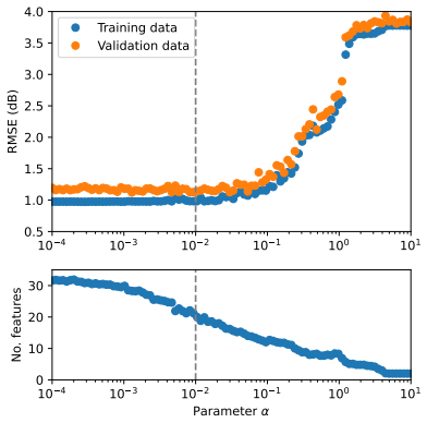
- [Section 3.3] In Figure 2, the x-axis label 'Parameter' should explicitly identify the LASSO regularization parameter alpha, and the axis scale should be marked as logarithmic.
- [Section 3.6] The ANN hyperparameter is written as 'n_layer' in the text but 'n_layers' in the architecture description; please use consistent notation.
Circularity Check
No material circularity: model benchmarking uses held-out nested cross-validation, and the wavelength claim is tested by an independent annealing experiment; only a minor non-load-bearing self-citation appears.
full rationale
The paper's central derivation chain is not circular. The regression models are explicitly fit on training folds and evaluated on held-out validation folds via 10-fold nested cross-validation with 50 repetitions (Section 4), so the reported RMSE comparisons are genuine out-of-sample benchmarks rather than refits of the training data. The wavelength attribution is read from the refitted coefficient b14 in Table 2, but Section 5 then tests that attribution with a new post-fabrication annealing experiment performed at 1550 nm on devices not used to derive the model; the observed ~2 dB propagation-loss reduction is independent evidence for the N-H absorption mechanism. No parameter is fit to the annealed outcome and then called a prediction. The only self-citation is Ref. [21], used to justify the waveguide cutback technique; cutback is a standard external method and this citation does not carry the paper's central benchmarking or mitigation claims. Potential weaknesses such as pooling devices across wafers/runs and the absence of error bars in Figure 6 are threats to causal identification and external validity, not cases where a result reduces by definition to its inputs. Accordingly, the paper is self-contained with respect to its main derivation chain and receives a low score reflecting only the minor self-citation.
Assumptions & free parameters
free parameters (15)
- Intercept b =
4.3(1) dB
- WG Length coefficient b1 =
3.44(3) dB/cm
- Length x Wavelength [1600 nm] coefficient b14 =
-2.34(4) dB/cm
- Length x Polarization [TM] coefficient b15 =
-1.05(2) dB/cm
- Length x Wavelength [1600 nm] x Polarization [TM] coefficient b145 =
0.85(2) dB/cm
- Length x Polishing [with CMP] coefficient b13 =
-0.30(1) dB/cm
- WG Width [1.5 um] coefficient b2 =
0.4(1) dB
- Number of selected variables N =
7
- LASSO regularization alpha =
0.01
- Maximum tree depth for decision tree and random forest =
8
- SVR epsilon =
1.0
- SVR C =
30
- KRR regularization parameter (1/(2 alpha)) =
30
- ANN number of layers =
3
- ANN number of neurons =
64
assumptions (6)
- standard math Least squares fitting and p-value/F-statistic rankings are valid proxies for variable importance.
- domain assumption Insertion loss decomposes linearly into propagation loss and coupling loss with waveguide length via the cutback technique.
- domain assumption Waveguide loss depends linearly on length with no self-interacting terms, following the Beer-Lambert law.
- domain assumption N-H stretching bond absorption peaks near 1520 nm and annealing above 1000°C reduces this absorption.
- ad hoc to paper Devices with >40 dB loss are defective and can be excluded from analysis.
- domain assumption The dataset is representative and features are almost equally distributed, with duplicate devices capturing fabrication variability.
Cite this review
Pith. "Pith review of Analysis of Photonic Circuit Losses with Machine Learning Techniques." pith.science (2026). https://pith.science/paper/JTW7Z3IH
@misc{pith2026250617999,
  author       = {Pith},
  title        = {Pith review of: Analysis of Photonic Circuit Losses with Machine Learning Techniques},
  year         = {2026},
  howpublished = {\url{https://pith.science/paper/JTW7Z3IH}},
  note         = {Machine review of arXiv:2506.17999}
}
read the original abstract
Low-loss waveguides enable efficient light delivery in photonic circuits, which are essential for high-speed optical communications and scalable implementations of photonic quantum technologies. We study the effects of several fabrication and experimental parameters on the waveguide losses of a silicon nitride integrated photonics platform using various machine learning techniques. Compared to more complex machine learning algorithms, our results show that a simple linear regression model with variable selection offers a lower prediction error with high interpretability. The high interpretability, along with our domain knowledge, led to unique identification of fabrication process dependencies on the final outcome. With these insights, we show that by improving the process flow, it is possible to improve the loss by mitigating the cause in a real experiment.
Figures


Figures from the paper (3 more)


Reference graph
Works this paper leans on
-
[1]
Review of silicon photonics technology and platform development,
S. Y. Siew, B. Li, F. Gao,et al., “Review of silicon photonics technology and platform development,” J. Light. Technol.39, 4374–4389 (2021)
work page 2021
-
[2]
J. X. B. Sia, X. Li, J. Wang,et al., “Wafer-scale demonstration of low-loss (∼0.43 dB/cm), high-bandwidth (>38 GHz), silicon photonics platform operating at the C-band,” IEEE Photonics J.14, 1–9 (2022)
work page 2022
-
[3]
J. Liu, G. Huang, R. N. Wang,et al., “High-yield, wafer-scale fabrication of ultralow-loss, dispersion-engineered silicon nitride photonic circuits,” Nat. communications12, 2236 (2021)
work page 2021
-
[4]
Z. Ye, H. Jia, Z. Huang,et al., “Foundry manufacturing of tight-confinement, dispersion-engineered, ultralow-loss silicon nitride photonic integrated circuits,” Photonics Res.11, 558–568 (2023)
work page 2023
-
[5]
J. W. Silverstone, D. Bonneau, J. L. O’Brien, and M. G. Thompson, “Silicon quantum photonics,” IEEE J. Sel. Top. Quantum Electron.22, 390–402 (2016)
work page 2016
-
[6]
Silicon nitride passive and active photonic integrated circuits: trends and prospects,
C. Xiang, W. Jin, and J. E. Bowers, “Silicon nitride passive and active photonic integrated circuits: trends and prospects,” Photonics Res.10, A82–A96 (2022)
work page 2022
-
[7]
Capturing the effects of spatial process variations in silicon photonic circuits,
Y. Xing, J. Dong, U. Khan, and W. Bogaerts, “Capturing the effects of spatial process variations in silicon photonic circuits,” ACS Photonics10, 928–944 (2022)
work page 2022
-
[8]
Process variation in silicon photonic devices,
X. Chen, M. Mohamed, Z. Li,et al., “Process variation in silicon photonic devices,” Appl. optics52, 7638–7647 (2013)
work page 2013
Show all 45 references
-
[9]
Optical quantum computing,
J. L. O’brien, “Optical quantum computing,” Science318, 1567–1570 (2007)
2007
-
[10]
Nanoscale low crosstalk photonic crystal integrated sensor array,
D. Yang, H. Tian, and Y. Ji, “Nanoscale low crosstalk photonic crystal integrated sensor array,” IEEE Photonics J.6, 1–7 (2014)
2014
-
[11]
Performancepredictionforsiliconphotonicsintegratedcircuitswithlayout-dependent correlated manufacturing variability,
Z.Lu,J.Jhoja,J.Klein, et al.,“Performancepredictionforsiliconphotonicsintegratedcircuitswithlayout-dependent correlated manufacturing variability,” Opt. express25, 9712–9733 (2017)
2017
-
[12]
Modelling fabrication variability in silicon photonic devices
M. A. Hamdani and G. Qazi, “Modelling fabrication variability in silicon photonic devices.” Photonic Materials: Recent Adv. Emerg. Appl. p. 265 (2023)
2023
-
[13]
Advances in machine learning for large-scale manufacturing of photonic circuits,
K. Yadav, S. Bidnyk, and A. Balakrishnan, “Advances in machine learning for large-scale manufacturing of photonic circuits,” inEPJ Web of Conferences,vol. 287 (EDP Sciences, 2023), p. 13004
2023
-
[14]
Machine learning for mask/wafer hotspot detection and mask synthesis,
Y. Lin, X. Xu, J. Ou, and D. Z. Pan, “Machine learning for mask/wafer hotspot detection and mask synthesis,” in Photomask Technology 2017,vol. 10451 (SPIE, 2017), pp. 72–84
2017
-
[15]
Use of neural network to model the deposition rate of PECVD-silicon nitride films,
B. Kim, K. Park, and D. Lee, “Use of neural network to model the deposition rate of PECVD-silicon nitride films,” Plasma Sources Sci. Technol.14, 83 (2005)
2005
-
[16]
Regression methods for prediction of PECVD silicon nitride layer thickness,
H. Purwins, A. Nagi, B. Barak,et al., “Regression methods for prediction of PECVD silicon nitride layer thickness,” in 2011 IEEE International Conference on Automation Science and Engineering, (IEEE, 2011), pp. 387–392
2011
-
[17]
Neural network modeling of inter-characteristics of silicon nitride film deposited by using a plasma-enhanced chemical vapor deposition,
S. J. Lee, B. Kim, and S. W. Baik, “Neural network modeling of inter-characteristics of silicon nitride film deposited by using a plasma-enhanced chemical vapor deposition,” Expert Syst. with Appl.38, 11437–11441 (2011)
2011
-
[18]
Evaluating regression-based techniques for modelling fabrication variations in silicon photonic waveguides,
A. E. James, A. Wang, S. Wang, and K. Bergman, “Evaluating regression-based techniques for modelling fabrication variations in silicon photonic waveguides,” inApplications of Machine Learning 2021, vol. 11843 (SPIE, 2021), pp. 18–23
2021
-
[19]
Random forest modelling as a tool for propagation and bend excess loss minimization on silicon nitride waveguide platforms,
J. W. Hinum-Wagner, S. M. Hoermann, G. Feigl,et al., “Random forest modelling as a tool for propagation and bend excess loss minimization on silicon nitride waveguide platforms,” inMachine Learning in Photonics, vol. 13017 (SPIE, 2024), pp. 216–230
2024
-
[20]
Deep learning models for effective refractive indices in silicon nitride waveguides,
G. Alagappan and C. E. Png, “Deep learning models for effective refractive indices in silicon nitride waveguides,” J. Opt.21, 035801 (2019)
2019
-
[21]
Improved waveguide surface roughness by foundry-processing techniques for enhanced light delivery to integrated ion trap for quantum computing platforms,
S. C. Goh, A. N. Utama, H. Yu,et al., “Improved waveguide surface roughness by foundry-processing techniques for enhanced light delivery to integrated ion trap for quantum computing platforms,” inOptical Interconnects XXIV,vol. 12892 (SPIE, 2024), pp. 87–93
2024
-
[22]
A study of cross-validation and bootstrap for accuracy estimation and model selection,
R. Kohaviet al., “A study of cross-validation and bootstrap for accuracy estimation and model selection,” inIjcai, vol. 14(2) (Montreal, Canada, 1995), pp. 1137–1145
1995
-
[23]
Linearregression,
G.James,D.Witten,T.Hastie, et al.,“Linearregression,”in An introduction to statistical learning: With applications in python, (Springer, 2023), pp. 69–134
2023
-
[24]
A survey of feature selection and feature extraction techniques in machine learning,
S. Khalid, T. Khalil, and S. Nasreen, “A survey of feature selection and feature extraction techniques in machine learning,” in2014 science and information conference, (IEEE, 2014), pp. 372–378
2014
-
[25]
Regression modeling strategies,
F. E. Harrell, “Regression modeling strategies,” R package version pp. 6–2 (2012)
2012
-
[26]
Generalized linear models,
J. A. Nelder and R. W. Wedderburn, “Generalized linear models,” J. Royal Stat. Soc. Ser. A: Stat. Soc.135, 370–384 (1972)
1972
-
[27]
Regression shrinkage and selection via the lasso,
R. Tibshirani, “Regression shrinkage and selection via the lasso,” J. Royal Stat. Soc. Ser. B: Stat. Methodol.58, 267–288 (1996)
1996
-
[28]
Induction of decision trees,
J. R. Quinlan, “Induction of decision trees,” Mach. learning1, 81–106 (1986)
1986
-
[29]
Random forests,
L. Breiman, “Random forests,” Mach. learning45, 5–32 (2001)
2001
-
[30]
Scikit-learn: Machine learning in python,
F. Pedregosa, G. Varoquaux, A. Gramfort,et al., “Scikit-learn: Machine learning in python,” J. machine learning research12, 2825–2830 (2011)
2011
-
[31]
A tutorial on support vector regression,
A. J. Smola and B. Schölkopf, “A tutorial on support vector regression,” Stat. computing14, 199–222 (2004)
2004
-
[32]
Kernel ridge regression,
V. Vovk, “Kernel ridge regression,” inEmpirical inference: Festschrift in honor of vladimir n. vapnik, (Springer, 2013), pp. 105–116
2013
-
[33]
TensorFlow: Large-scale machine learning on heterogeneous systems,
M. Abadi, A. Agarwal, P. Barham,et al., “TensorFlow: Large-scale machine learning on heterogeneous systems,” (2015). Software available from tensorflow.org
2015
-
[34]
Adam: A method for stochastic optimization,
D. P. Kingma and J. Ba, “Adam: A method for stochastic optimization,” arXiv preprint arXiv:1412.6980 (2014)
2014 arXiv
-
[35]
No unbiased estimator of the variance of k-fold cross-validation,
Y. Bengio and Y. Grandvalet, “No unbiased estimator of the variance of k-fold cross-validation,” Adv. Neural Inf. Process. Syst.16(2003)
2003
-
[36]
On estimating model accuracy with repeated cross-validation,
G. Vanwinckelen and H. Blockeel, “On estimating model accuracy with repeated cross-validation,” inBeneLearn 2012: Proceedings of the 21st Belgian-Dutch conference on machine learning, (2012), pp. 39–44
2012
-
[37]
Cross-validation: what does it estimate and how well does it do it?
S. Bates, T. Hastie, and R. Tibshirani, “Cross-validation: what does it estimate and how well does it do it?” J. Am. Stat. Assoc.119, 1434–1445 (2024)
2024
-
[38]
Plasma enhanced chemical vapor deposition silicon oxynitride optimized for application in integrated optics,
K. Wörhoff, A. Driessen, P. Lambeck,et al., “Plasma enhanced chemical vapor deposition silicon oxynitride optimized for application in integrated optics,” Sensors Actuators A: Phys.74, 9–12 (1999)
1999
-
[39]
Comparative investigation of hydrogen bonding in silicon based PECVD grown dielectrics for optical waveguides,
F. Ay and A. Aydinli, “Comparative investigation of hydrogen bonding in silicon based PECVD grown dielectrics for optical waveguides,” Opt. materials26, 33–46 (2004)
2004
-
[40]
Low loss Si3N4-SiO2 optical waveguides on Si,
C. H. Henry, R. F. Kazarinov, H. J. Lee,et al., “Low loss Si3N4-SiO2 optical waveguides on Si,” Appl. optics26, 2621–2624 (1987)
1987
-
[41]
Nonlinear silicon nitride waveguides based on a PECVD deposition platform,
L. Wang, W. Xie, D. Van Thourhout,et al., “Nonlinear silicon nitride waveguides based on a PECVD deposition platform,” Opt. express26, 9645–9654 (2018)
2018
-
[42]
CMOS compatible monolithic multi-layer Si3N4-on-SOI platform for low-loss high performance silicon photonics dense integration,
Y. Huang, J. Song, X. Luo,et al., “CMOS compatible monolithic multi-layer Si3N4-on-SOI platform for low-loss high performance silicon photonics dense integration,” Opt. Express22, 21859–21865 (2014)
2014
-
[43]
Material and optical properties of low-temperature NH3-free PECVD SiNx layers for photonic applications,
T. D. Bucio, A. Z. Khokhar, C. Lacava,et al., “Material and optical properties of low-temperature NH3-free PECVD SiNx layers for photonic applications,” J. Phys. D: Appl. Phys.50, 025106 (2016)
2016
-
[44]
Asurveyofdeepneuralnetworkarchitecturesandtheirapplications,
W.Liu,Z.Wang,X.Liu, et al.,“Asurveyofdeepneuralnetworkarchitecturesandtheirapplications,”Neurocomputing 234, 11–26 (2017)
2017
-
[45]
The Beer-Lambert law,
D. F. Swinehart, “The Beer-Lambert law,” J. chemical education39, 333 (1962)
1962
Reviewed August 6, 2026 · model on record in the stance chip above.
Discussion (0). Continue with ORCID to comment.