REVIEW 3 major objections 5 minor 59 references
Mechanical behavior of InP twinning superlattice nanowires
T0 review · 3 major / 5 minor · reviewed 2026-08-14 · deepseek-v4-flash
Pith's one-line read Taper-free InP twinning-superlattice nanowires loaded in tension along [111] deform elastically until they fracture in a brittle manner along a twin boundary, with measured modulus 87 ± 17 GPa, failure strain 2.9 ± 0.3%, and tensile…
desk verdict First tensile data on taper-free InP twinning-superlattice nanowires, but the twin-boundary fracture claim outruns the evidence. read the letter →
The pith
A machine-rendered reading of the paper's core claim, the machinery that carries it, and where it could break.
The reading
What carries the argument
The load-bearing object is the twinning superlattice itself: a nanowire containing a periodic array of twin boundaries spaced about 13 nm apart, grown along the close-packed [111] direction. The twin boundaries act as the preferred fracture path, and their intersection with the nanowire surface is the crack nucleation site. The experimental platform is a push-to-pull device inside a transmission electron microscope: a diamond flat punch pushes a semicircular end, the device converts that compression into tension across a central gap, and the nanowire is welded across the gap with platinum; the net force on the nanowire is obtained by subtracting the device's reaction force from the raw measured force, following the authors' earlier calibration. Molecular dynamics simulations with an InP interatomic potential, whose input elastic constants come from density functional theory, provide the atomistic picture of crack initiation and propagation that supports the interpretation of the TEM observations.
What would settle it
Perform the same tensile test on an identical InP twinning-superlattice nanowire using a force sensor that measures the nanowire load directly (for example, a MEMS tensile stage with integrated load cell) rather than subtracting the push-to-pull reaction force; a modulus outside 87 ± 17 GPa or any nonlinearity or dislocation activity before fracture would contradict the paper's elastic-brittle claim.
Extended reading notes
Core claim
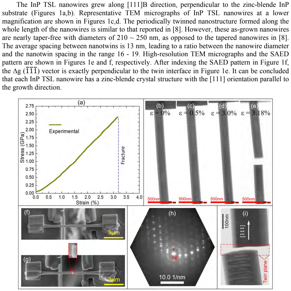
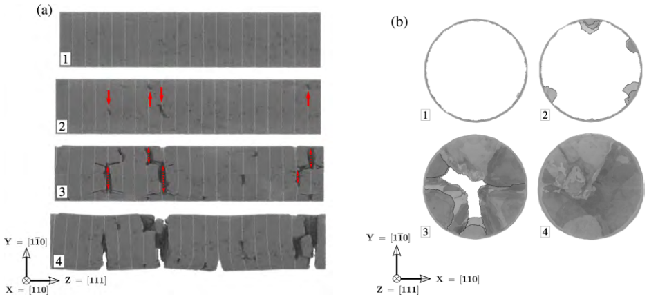
The central claim is that twinning-superlattice InP nanowires loaded in uniaxial tension along [111] show no inelastic deformation at any stage before failure: every stress–strain curve is linear up to fracture, and in situ TEM images show no dislocation activity, necking, or bending even at strains near 3%. Fracture is brittle and occurs by nucleation and propagation of a crack along a twin-boundary plane, with the crack starting at the nanowire surface at the intersection with the twin boundary. From a small set of successful tests, the paper reports E[111] = 87 ± 17 GPa, failure strain 2.9 ± 0.3%, and tensile strength 2.15–2.90 GPa over diameters of 210–250 nm. Molecular dynamics simulations of twinned nanowires also fracture without inelastic mechanisms, with cracks initiating at twin-boundary/surface intersections and propagating along the twin plane; the simulations give a higher strength (~6.7–6.9 GPa) than experiments, which the paper explains by the stress concentration from the zig-zag surface waviness at twin boundaries.
Load-bearing premise
The result rests on the assumption that the net force on the nanowire equals the raw measured force minus the push-to-pull device's reaction force, i.e., that mounting and welding the nanowire do not change the device's stiffness or add a spurious load path; if this subtraction is wrong, the reported modulus and strength are systematically off.
Editorial extensions
If this is right
- Designers of InP nanowire devices should treat tensile loads along [111] as limited to about 2.1–2.9 GPa and to elastic strains below about 3%, since failure is abrupt and pre-fracture plasticity cannot absorb energy.
- Twin boundaries are the weakest links in these nanowires: the fracture plane is always a twin boundary, so controlling twin spacing and surface smoothness, rather than bulk crystal strength, sets the practical strength.
- The measured elastic modulus (87 ± 17 GPa) is the value to use in bending or resonance analyses of TSL InP nanowires; the presence of twins does not appear to change the stiffness compared with untwinned material.
- Molecular dynamics predicts a strength of 6.7–6.9 GPa for perfect twinned nanowires, so the gap between simulation and experiment indicates that removing surface waviness could raise real nanowire strength toward that range.
- Because fracture leaves a flat surface perpendicular to the growth direction, post-fracture inspection of a failed device can diagnose whether overload was tensile along the nanowire axis.
Reading between the lines
- If the twin boundary is genuinely the weakest plane, then deliberately engineering twin spacing or removing surface notches could raise strength, an avenue the paper does not test.
- The absence of plasticity at ~0.02 s−1 strain rate does not rule out dislocation activity at slower rates, higher temperatures, or under cyclic loading; a rate-dependent transition is a testable extension.
- The same push-to-pull methodology could be applied to other III–V superlattice nanowires (e.g., GaAs or InP/InAs heterostructures) to check whether brittle twin-boundary fracture is generic to zinc-blende superlattices.
- The reported 'smaller is stronger' trend over only three diameters is suggestive but not established; testing more diameters would settle whether a real size effect exists.
Signed reviews
Editorial analysis
A structured set of objections, weighed in public.
Referee Report
Summary. The paper reports in situ transmission electron microscope (TEM) tensile tests of three taper-free InP twinning-superlattice (TSL) nanowires grown along the [111] direction, with diameters of 210–250 nm and an average twin spacing of about 13 nm. The measured stress-strain curves are linear to failure, yielding an elastic modulus of 87 ± 17 GPa, a failure strain of 2.9 ± 0.3%, and tensile strengths of 2.15–2.90 GPa. Fracture surfaces are flat and perpendicular to the growth direction, and the authors conclude that fracture occurred by brittle crack propagation along a twin boundary. Molecular dynamics (MD) simulations using a Vashishta-type interatomic potential show, for idealized twinned nanowires, crack nucleation at the twin boundary/surface intersection and propagation along the twin plane, with no inelastic deformation prior to failure. The paper's central claims are that InP TSL nanowires deform purely elastically until brittle failure and that the fracture path is the twin boundary.
Significance. If the results hold, this is the first tensile mechanical characterization of taper-free InP twinning-superlattice nanowires, providing quantitative design data (elastic modulus, failure strain, strength) relevant to InP nanowire-based devices. The work combines careful in situ TEM experiments with DFT-validated elastic constants and MD simulations, and the supplementary videos provide direct evidence of linear, uniaxial deformation up to ~3% strain. The authors are appropriately cautious about the limited number of tests and state that a size effect cannot be concluded. However, the central mechanistic claim—that fracture propagates specifically along a twin boundary—is not uniquely established by the experimental evidence, and the quantitative agreement between MD and experiment is weak; these limitations materially affect the strength of the conclusions drawn in the abstract and conclusions.
major comments (3)
- [Section 3.2, Figures 3h and 3i] The claim that fracture occurred 'along the twin boundary' is not uniquely supported by the evidence presented. The flat fracture surface perpendicular to [111] and the Δg vector nearly parallel to [111] only establish that the crack plane is a {111} plane, which is also the orientation of every twin boundary in this geometry and of ordinary {111} cleavage in zinc-blende InP. The in situ TEM images in Figures 3b–e stop at 3.0% strain, before the fracture at 3.18%, so the crack path was not directly observed. The MD simulations in Section 3.3 show twin-boundary fracture in an idealized geometry, but they do not by themselves prove that the experimental crack followed a twin boundary. Please provide high-resolution evidence of the fracture surface or trace (e.g., HRTEM of the fracture edge or of both fracture halves) or soften the central claim to fracture on a {111} plane, with twin-boundary fracture as a plausible interpretation consistent with MD.
- [Section 2.2, Figure 2g, Table 1] The reported values of elastic modulus, failure strain, and strength rest on the force calibration in which the net nanowire force is obtained by subtracting the PTP-device reaction force measured in the authors' previous work (Ref. 36). No verification is provided that the PTP frame stiffness is unchanged after mounting and welding the nanowire, and a systematic error in this subtraction would shift all reported mechanical properties. In addition, Table 1 contains only three nanowires, with elastic moduli of 77.9, 78.4, and 104 GPa, i.e., 87 ± 17 GPa; this large scatter and small sample size limit the statistical significance of the mean values and of the apparent strength increase with decreasing diameter. Please state the uncertainty budget and, if possible, validate the calibration with a reference sample or an independent measurement.
- [Section 3.3, Figure S3] The MD simulations do not cover the experimental parameter range: the simulated nanowires have D = 24 nm and D/l from 2 to 12, while the experiments have D ≈ 210–250 nm and D/l ≈ 16–19; the MD strain rate (10^9 s^-1) is about eight orders of magnitude above the experimental strain rate (~0.02 s^-1), and the simulated strength (6.7–6.9 GPa) is 2.3–3 times the measured strength (2.15–2.90 GPa). The attribution of this discrepancy to 'zig-zag waviness' at the twin boundaries is not quantitatively substantiated, since the notch radius at the twin boundary was not measured. The simulations therefore provide qualitative mechanistic insight but cannot be used to validate the experimental strength values; this limitation should be stated explicitly in the comparison between simulations and experiments.
minor comments (5)
- [Section 2.2] The text says 'according to the design of the PTPT device [36]'; 'PTPT' appears to be a typo and should read 'PTP device'.
- [Section 3.2, Figure 3h] The caption states that the TEM beam direction is 'very close to the [111] zone axis'; since the SAED pattern is indexed, please clarify whether the beam direction is exactly [111] or slightly off-axis, and define how Δg was measured.
- [Section 3.1] For clarity, state explicitly that the diameter-to-twin-spacing ratio of 16–19 corresponds to diameters of 210–250 nm and a twin spacing of 13 nm, and note that this ratio is outside the simulated D/l range.
- [Section 2.3 and Table 2] The description of the MD simulations omits the Vashishta potential parameters and the procedure for constructing the twinned supercells; please provide these details or reference them explicitly in the Supplementary Material.
- [References] Some reference entries contain typographical errors, e.g., 'Scipta Mater.' (Ref. 22) should be 'Scripta Mater.', and 'PANS' (Ref. 54) should be 'PNAS'.
Circularity Check
No circular derivation found; the experimental measurements and the MD simulations are independent.
full rationale
The paper's central experimental results—the elastic modulus, failure strain, and tensile strength—are obtained directly from in situ TEM tensile tests. The net nanowire force is derived by subtracting the PTP device reaction force following the calibration in the authors' previous work (Ref. 36), but that calibration is an independent device characterization, not a fit to the InP nanowire data, and it does not presuppose the reported mechanical properties. The MD simulations use a literature interatomic potential (Vashishta et al.) and DFT-derived lattice parameters; no parameter is fitted to the measured stress-strain curves, so the simulated response is an independent prediction rather than an input. The claim that fracture occurred along a twin boundary is inferred from post-mortem SAED and the flat fracture-surface morphology and is then supported, not defined, by the MD crack-propagation images. While the experimental evidence for the twin-boundary fracture path may be open to alternative interpretation, such as cleavage on another {111} plane, that is an evidentiary limitation rather than a circular derivation. No equation, fitted parameter, or self-citation chain reduces the paper's conclusions to their own premises.
Assumptions & free parameters
free parameters (1)
- Vashishta InP interatomic potential parameters =
not specified in this paper; from Vashishta et al. 2007
assumptions (4)
- domain assumption The Vashishta interatomic potential faithfully reproduces InP elastic behavior and fracture mechanisms.
- domain assumption DFT-GGA/PBE with PAW pseudopotentials gives accurate elastic constants and stacking fault energy for InP.
- domain assumption The net force on the nanowire equals the raw force minus the PTP device reaction force, with unchanged frame stiffness.
- ad hoc to paper Zig-zag surface waviness at twin boundaries is the main cause of the experimental strength being much lower than MD strength.
Cite this review
Pith. "Pith review of Mechanical behavior of InP twinning superlattice nanowires." pith.science (2026). https://pith.science/paper/KSV3X6WR
@misc{pith2026190811239,
  author       = {Pith},
  title        = {Pith review of: Mechanical behavior of InP twinning superlattice nanowires},
  year         = {2026},
  howpublished = {\url{https://pith.science/paper/KSV3X6WR}},
  note         = {Machine review of arXiv:1908.11239}
}
read the original abstract
Taper-free InP twinning superlattice (TSL) nanowires with an average twin spacing of ~ 13 nm were grown along the zinc-blende close-packed [111] direction using metalorganic vapor phase epitaxy. The mechanical properties and fracture mechanisms of individual InP TSL nanowires in tension were ascertained by means of in situ uniaxial tensile tests in a transmission electron microscope. The elastic modulus, failure strain and tensile strength along the [111] direction were determined. No evidence of inelastic deformation mechanisms was found before fracture, which took place in a brittle manner along the twin boundary. The experimental results were supported by molecular dynamics simulations of the tensile deformation of the nanowires that also showed that the fracture of twinned nanowires occurred in the absence of inelastic deformation mechanisms by the propagation of a crack from the nanowire surface along the twin boundary.
Figures
Reference graph
Works this paper leans on
-
[1]
Nature 2001, 409, 66-69, DOI: 10.1038/35051047
Duan X.; Huang Y.; Cui Y.; Wang J.; Lieber C.M. Nature 2001, 409, 66-69, DOI: 10.1038/35051047
-
[2]
Bao J.; Bell D.C.; Capasso F. Nano Lett. 2008, 8(3) 836-841, DOI: 10.1021/nl072921e
-
[3]
ACS Nano 2016, 10(12), 11414-11419, DOI: 10.1021/acsnano.6b06874
van Dam D.; van Hoof N.J.J.; Cui Y.; et al. ACS Nano 2016, 10(12), 11414-11419, DOI: 10.1021/acsnano.6b06874
-
[4]
Ikejiri K.; Kitauchi Y.; Tomioka K.; Motohisa J.; Fukui T. Nano Lett. 2011, 11, 4314-4318, DOI: 10.1021/nl202365q
-
[5]
Yan X.; Zhang X.; Li J.; Wu Y.; Ren X. Appl. Phys. Lett. 2015, 101, 023101, DOI: 10.1063/1.4926728
- [6]
-
[7]
Janissen R.; Sahoo P.K.; Santos C.A.; da Silva A.M.; von Zuben A.A.G.; Souto D.E.P.; Costa A.D.T.; Celedon P.; Zanchin N.I.T.; Almeida D.B.; Oliveira D.S.; Kubota L.T.; Cesar C.L.; de Souza A.P.; Cotta M.A. Nano Lett. 2017, 17, 5938-5949, DOI: 10.1021/acs.nanolett.7b01803
-
[8]
Nature 2008, 456, 369-372, DOI: 10.1038/nature07570
Algra R.E.; Verheijen M.A.; Borgström M.T.; Feiner L.; Immink G.; van Enckevort W.J.P.; Vlieg E.; Bakkers E.P.A.M. Nature 2008, 456, 369-372, DOI: 10.1038/nature07570
Show all 59 references
-
[9]
Nature Mater
Johansson J.; Karlsson L.S.; Svensson C.P.T.; Martensson T.; Wacaser B.A.; Deppert K.; Samuelson L.; Seifert W. Nature Mater. 2006, 5, 574-580, DOI: 10.1038/nmat1677
2006 doi
-
[10]
Nano Lett
Chen B.; Wang J.; Gao Q.; Chen Y.; Liao X.; Lu C.; Tan H.H.; Mai Y.W.; Zou J.; Ringer S.P.; Gao H.; Jagadish C. Nano Lett. 2013, 13, 4369-4373, DOI: 10.1021/nl402180k
2013 doi
-
[11]
Ikonic Z.; Srivastava G.P.; Inkson J.C. Phys. Rev. B 1993, 48, 17181-17193, DOI: 10.1103/PhysRevB.48.17181
1993 doi
-
[12]
Ikonic Z.; Srivastava G.P.; Inkson J.C. Phys. Rev. 1995, 52, 14078-14085, DOI: 10.1103/PhysRevB.52.14078
1995 doi
-
[13]
Fissel A.; Bugiel E.; Wang C.R.; Osten H.J. J. Cryst. Growth 2006, 290, 392-397, DOI: 10.1016/j.jcrysgro.2006.02.009 11
2006 doi
-
[14]
Nano Lett
Hao Y.; Meng G.; Wang Z.L.; Ye C.; Zhang L. Nano Lett. 2006, 6, 1650-1655, DOI: 10.1021/nl060695n
2006 doi
-
[15]
Nature Nanotech
Yang R.; Qin Y.; Dai L.; Wang Z.L. Nature Nanotech. 2009, 4, 34-39, DOI: 10.1038/nnano.2008.314
2009 doi
-
[16]
Nature 2011, 479, 324-328, DOI: 10.1038/nature10678
Pillarisetty R. Nature 2011, 479, 324-328, DOI: 10.1038/nature10678
2011 doi
-
[17]
Chu M.; Sun Y.; Aghoram U.; Thompson S.E. Annu. Rev. Mater. Res. 2009, 39, 203-229, DOI: 10.1146/annurev-matsci-082908-145312
2009 doi
-
[18]
Koga T.; Sun X.; Cronin S.B.; Dresselhaus M.S. Appl. Phys. Lett. 1999, 75, 2438-2440, DOI: 10.1063/1.125040
1999 doi
-
[19]
Science 2018, 360(6386), 264-265, DOI: 10.1126/science.aat5211
Llorca J. Science 2018, 360(6386), 264-265, DOI: 10.1126/science.aat5211
2018 doi
-
[20]
Nano Lett
Huang J.Y.; Zheng H.; Mao S.X.; Li Q.; Wang G.T. Nano Lett. 2011, 11, 1618-1622, DOI: 10.1021/nl200002x
2011 doi
-
[21]
Nature Mater
Kiener D.; Hosemann P.; Maloy S.A.; Minor A.M. Nature Mater. 2011, 10, 608-613, DOI: 10.1038/nmat3055
2011 doi
-
[22]
Scipta Mater
Jawaharram G.S.; Price P.M.; Barr C.M.; Hattar K.; Averback R.S.; Dillon S.J. Scipta Mater. 2018, 148, 1-4, DOI: 10.1016/j.scriptamat.2018.01.007
2018 doi
-
[23]
Nano Lett
Chen Y.; Burgess T.; An X.; Mai Y.W.; Tan H.H.; Zou J.; Ringer S.P.; Jagadish C.; Liao X. Nano Lett. 2016, 16(3), 1911-1916, DOI: 10.1021/acs.nanolett.5b05095
2016 doi
-
[24]
Wang Y.B.; Wang L.F.; Joyce H.J.; Cao Q.; Liao X.Z.; Mai Y.W.; Tan H.H.; Zou J.; Ringer S.P.; Gao H.J.; Jagadish C. Adv. Mater. 2011, 23, 1356-1360, DOI: 10.1002/adma.201004122
2011 doi
-
[25]
Nano Lett
Dunaevskiy M.; Geydt P.; Lähderanta E.; Alekseev P.; Haggrén T.; Kakko J.P.; Jiang H.; Lipsanen H. Nano Lett. 2017, 17, 3441-3446, DOI: 10.1021/acs.nanolett.7b00312
2017 doi
-
[26]
Scripta Mater
Wang L.; Teng J.; Kong D.; Yu G.; Zou J.; Zhang Z.; Han X. Scripta Mater. 2018, 147, 103- 107, DOI: 10.1016/j.scriptamat.2018.01.012
2018 doi
- [27]
-
[28]
Nano Lett
Seo J.H.; Yoo Y.; Park N.Y.; Yoon S.W.; Lee H.; Han S.; Lee S.W.; Seong T.Y.; Lee S.C.; Lee K.B.; Cha P.R.; Park H.S.; Kim B.; Ahn J.P. Nano Lett. 2011, 11(8), 3499-3502, DOI: 10.1021/nl2022306
2011 doi
-
[29]
Geydt P.; Dunaevskiy M.; Alekseev P.; Kakko J-P.; Haggren T.; Lahderanta E.; Lipsanen H. J. Phys. Conf. Ser. 2016, 769, 012029, DOI: 10.1088/1742-6596/769/1/012029
2016 doi
-
[30]
Zhu Y.; Chang T.H. J. Micromech. Microeng. 2015, 25, 093001, DOI: 10.1088/0960- 1317/25/9/093001
2015 doi
- [31]
-
[32]
Wang S.; Shan Z.; Huang H. Adv. Sci. 2017, 4, 1600332, DOI: 10.1002/advs.201600332
2017 doi
-
[33]
JOM 2009, 61(3), 24-34, DOI: 10.1007/s11837-009-0037-3
Gianola D.S.; Eberl C. JOM 2009, 61(3), 24-34, DOI: 10.1007/s11837-009-0037-3
2009 doi
-
[34]
Chen Y.J.; An X.H.; Liao X.Z. Appl. Phys. Rev. 2017, 4, 031104, DOI: 10.1063/1.4989649 12
2017 doi
-
[35]
Acta Mater
Chisholm C.; Bei H.; Lowry M.B.; Oh J.; Asif S.A.S.; Warren O.L.; Shan Z.W.; George E.P.; Minor A.M. Acta Mater. 2012, 60, 2258-2264, DOI: 10.1016/j.actamat.2011.12.027
2012 doi
-
[36]
Extreme Mech
Liu Z.; Monclús M.A.; Yang L.W.; Castillo-Rodríguez M.; Molina-Aldareguía J.M.; Llorca J. Extreme Mech. Lett. 2018, 25, 60-65, DOI: 10.1016/j.eml.2018.10.007
2018 doi
-
[37]
Han S.Z.; Kang J.; Kim S.D.; Choi S.Y.; Kim H.G.; Lee J.; Kim K.; Lim S.H.; Han B. Sci. Rep. 2015, 5, 15050, DOI: 10.1038/srep15050
2015 doi
-
[38]
ACS Nano 2012, 6(11), 9425-9432, DOI: 10.1021/nn3037623
Kushima A.; Huang J.Y.; Li J. ACS Nano 2012, 6(11), 9425-9432, DOI: 10.1021/nn3037623
2012 doi
-
[39]
Lu Y.; Song J.; Huang J.Y.; Lou J. Adv. Funct. Mater. 2011, 21, 3982-3989, DOI: 10.1002/adfm.201101224
2011 doi
-
[40]
Nano Lett
Agrawal R.; Peng B.; Espinosa H.D. Nano Lett. 2009, 9(12), 4177-4183, DOI: 10.1021/nl9023885
2009 doi
-
[41]
Nano Lett
Guo H.; Chen K.; Oh Y.; Wang K.; Dejoie C.; Asif S.A.S.; Warren O.L.; Shan Z.W.; Wu J.; Minor A.M. Nano Lett. 2011, 11, 3207-3213, DOI: 10.1021/nl201460v
2011 doi
-
[42]
Yuan X.; Guo Y.; Caroff P.; He J.; Tan H.H.; Jagadish C. Phys. Status Solidi-R Res. Lett. 2017, 1700310, DOI: 10.1002/pssr.201700310
2017 doi
-
[43]
Nature Mater
Chen L.Y.; He M.; Shin J.; Richter G.; Gianola D.S. Nature Mater. 2015, 14, 707-713, DOI: 10.1038/nmat4288
2015 doi
-
[44]
Paolo G.; Stefano B.; Nicola B.; et al. J. Phys.: Condens. Matter, 2009, 21, 395502, DOI: 10.1088/0953-8984/21/39/395502
2009 doi
-
[45]
Perdew J.P.; Burke K.; Ernzerhof M. Phys. Rev. Lett. 1996, 77(18), 3865-3868, DOI: 10.1103/PhysRevLett.77.3865
1996 doi
-
[46]
Blöchl P.E. Phys. Rev. B 1994, 50, 17953, DOI: 10.1103/PhysRevB.50.17953
1994 doi
-
[47]
Monkhorst H.J.; Pack J.D. Phys. Rev. B 1976, 13, 5188, DOI: 10.1103/PhysRevB.13.5188
1976 doi
-
[48]
Vashishta P.; Kalia R.K.; Nakano A.; Rino J.P. J. Appl. Phys. 2007, 101(10), 103515, DOI: 10.1063/1.2724570
2007 doi
-
[49]
LAMMPS-large-scale atomic/molecular massively parallel simulator, Sandia National Laboratories, 2007, 18, 43
Plimpton S.; Crozier P.; Thompson A. LAMMPS-large-scale atomic/molecular massively parallel simulator, Sandia National Laboratories, 2007, 18, 43
2007
-
[50]
Park H.S.; Gall K.; Zimmerman J.A. J. Mech. Phys. Solids 2006, 54, 1862-1881, DOI: 10.1016/j.jmps.2006.03.006
2006 doi
-
[51]
Pial T.H.; Rakib T.; Mojumder S.; Motalab M.; Akanda M.S. Phys. Chem. Chem. Phys. 2018, 20, 8647-8657, DOI: 10.1039/C7CP08252E
2018 doi
-
[52]
Tsai D. J. Chem. Phys. 1979, 70, 1375-1382, DOI: 10.1063/1.437577
1979 doi
-
[53]
Nano Lett
Tang D.M.; Ren C.L.; Wang M.S.; Wei X.; Kawamoto N.; Liu C.; Bando Y.; Mitome M.; Fukata N.; Golberg D. Nano Lett. 2012, 12(4), 1898-1904, DOI: 10.1021/nl204282y
2012 doi
-
[54]
PANS 2013, 110(33), 13289-13293, DOI: 10.1073/pnas.1306371110
Yu Q.; Qi L.; Mishra R.K.; Li J.; Minor A.M. PANS 2013, 110(33), 13289-13293, DOI: 10.1073/pnas.1306371110
2013 doi
-
[55]
Wei Y.J. Phys. Rev. B 2011, 84, 014107, DOI: 10.1103/PhysRevB.84.014107
2011 doi
-
[56]
Nature Nanotech
Jiang D.C.; Li X.Y.; Gao H.J.; Greer J.R. Nature Nanotech. 2012, 7, 594-601, DOI: 13 10.1038/nnano.2012.116
2012 doi
-
[57]
Dos Santos C.L.; Piquini P. Phys. Rev. B, 2010, 81, 075408, DOI: 10.1103/PhysRevB.81.075408
2010 doi
-
[58]
Physical properties of III-V semiconductor compounds, John Wiley & Sons, Chichester, UK, 1992
Adachi S. Physical properties of III-V semiconductor compounds, John Wiley & Sons, Chichester, UK, 1992
1992
-
[59]
Gottschalk H.; Patzer G.; Alexander H. Phys. Status Solidi-A 1978, 45(1), 207-217, DOI: 10.1002/pssa.2210450125 1 SUPPLEMENTARY MATERIAL Mechanical behavior of InP twinning superlattice nanowires Zhilin Liua, b, I. Papadimitrioub, M. Castillo-Rodríguezb, C. Wangb, G. Esteban-M...
1978 doi
Reviewed August 14, 2026 · model on record in the stance chip above.
Discussion (0). Continue with ORCID to comment.