Self-trapped holes and acceptor impurities in orthorhombic Ga2O3
Pith reviewed 2026-05-22 20:59 UTC · model grok-4.3
The pith
Self-trapped holes form readily in orthorhombic Ga2O3 and stabilize further with acceptor dopants.
A machine-rendered reading of the paper's core claim, the machinery that carries it, and where it could break.
Core claim
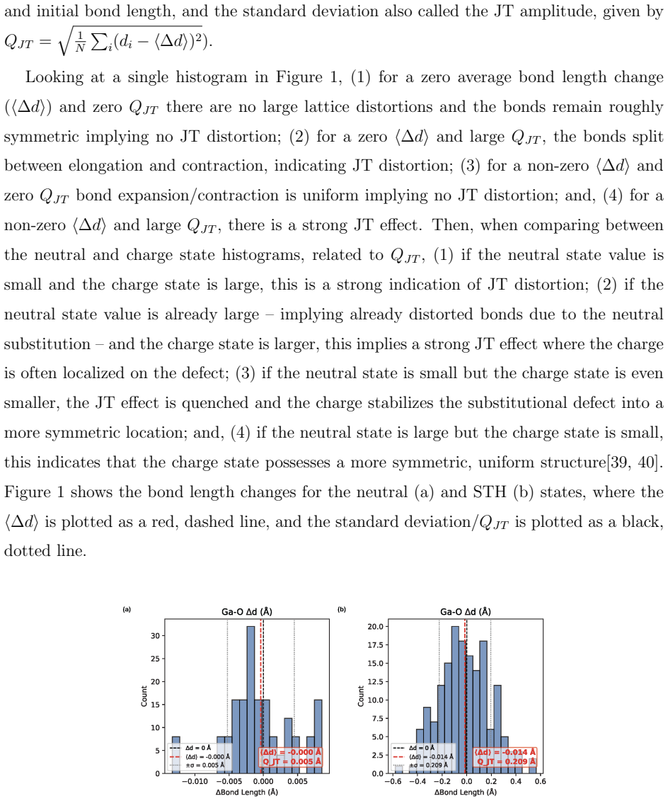
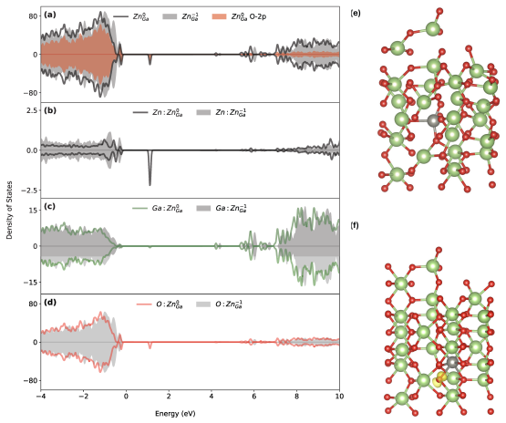
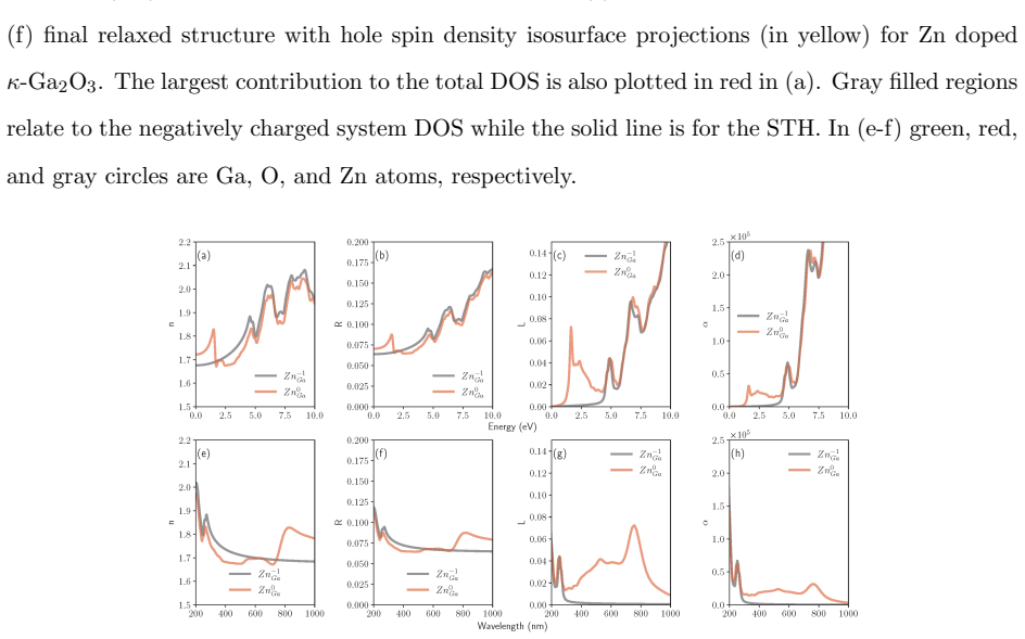
Hole trapping was found to be energetically favorable in all systems investigated and was further stabilized by acceptor dopants with large ionization energies. The electronic structures revealed emergent states in the band gap ranging from 0.2 to 1.2 eV above the valence band maximum, primarily composed of O 2p orbitals in all cases, with a notable contribution from Zn 3d orbitals in the Zn-doped system. Hole trapping resulted in a pronounced red shift and the emergence of additional absorption peaks, producing optical characteristics that were in closer agreement with experimental observations. In each system, the trapped hole localized near the dopant atom, predominantly on adjacent O 2p,
What carries the argument
Self-trapping of holes localized on adjacent oxygen atoms near dopants, producing O 2p-derived states inside the band gap together with local lattice distortions.
Load-bearing premise
The hybrid density functional theory calculations accurately capture the energetics and localization of self-trapped holes without significant errors from functional choice, supercell size, or finite-size corrections.
What would settle it
Spectroscopic measurement of the positions of emergent gap states (0.2-1.2 eV above the valence band) in doped samples, or direct observation of the predicted red shift plus extra absorption peaks, would confirm or refute the reported energies and optical changes.
Figures


read the original abstract
The electronic and optical properties of self-trapped holes in kappa-phase orthorhombic Ga2O3 in conjunction with isoelectronic and acceptor dopants were studied using hybrid density functional theory. Hole trapping was found to be energetically favorable in all systems investigated and was further stabilized by acceptor dopants with large ionization energies. The electronic structures revealed emergent states in the band gap ranging from 0.2 to 1.2 eV above the valence band maximum, primarily composed of O 2p orbitals in all cases, with a notable contribution from Zn 3d orbitals in the Zn-doped system. Hole trapping resulted in a pronounced red shift and the emergence of additional absorption peaks, producing optical characteristics that were in closer agreement with experimental observations. In each system, the trapped hole localized near the dopant atom, predominantly on adjacent O atoms, accompanied by local lattice distortions. The valence band remained largely non-dispersive even in the presence of a hole; hole states lied near the Fermi level for isoelectronic dopants and deeper in the band gap for acceptor dopants. These findings indicate that isoelectronic doping may find an avenue for p-type doping in this polymorph of Ga2O3 if a means to mitigate self-compensation is found.
Editorial analysis
A structured set of objections, weighed in public.
Referee Report
Summary. The manuscript presents hybrid density functional theory calculations on self-trapped holes in orthorhombic (kappa-phase) Ga2O3, examining their energetics and electronic structure both in the pristine material and in the presence of isoelectronic and acceptor impurities. The central findings are that hole trapping is energetically favorable in all systems investigated and is further stabilized by acceptor dopants with large ionization energies. Emergent gap states appear between 0.2 and 1.2 eV above the valence band maximum, primarily of O 2p orbital character (with Zn 3d contributions in the Zn-doped case), accompanied by local lattice distortions and a red shift in optical absorption that brings the spectra into closer agreement with experiment. The work suggests that isoelectronic doping may provide a pathway toward p-type conductivity if self-compensation can be mitigated.
Significance. If the reported stabilization energies and gap-state positions hold under variations in functional parameters and supercell size, the study would be significant for the field of wide-bandgap oxide semiconductors. It directly addresses the long-standing difficulty of achieving p-type doping in Ga2O3 by quantifying the role of self-trapped holes and their interaction with dopants. The orbital-resolved electronic-structure results and the predicted optical changes supply concrete, spectroscopy-accessible predictions, while the proposal of isoelectronic dopants as a potential mitigation strategy offers a new angle on doping engineering in this polymorph.
major comments (2)
- [Computational Methods] Computational Methods section: the hybrid functional mixing parameter is not stated and no convergence tests with respect to supercell size or finite-size corrections for charged defects are reported. Because the central claims rest on the relative formation energies that establish energetic favorability of hole trapping and on the precise positions of the O 2p-derived gap states (0.2–1.2 eV), these numerical details are load-bearing for the quantitative conclusions.
- [Results] Results section (optical properties paragraph): the assertion that hole trapping produces optical characteristics 'in closer agreement with experimental observations' is stated without a quantitative comparison (e.g., peak positions or integrated intensities) between the calculated absorption spectra and measured data. A direct side-by-side table or figure is required to substantiate this claim.
minor comments (2)
- [Abstract] Abstract: the clause 'hole states lied near the Fermi level' is grammatically incorrect and should read 'lie'.
- Figure captions and axis labels should be expanded to make the plotted quantities (formation energies, density of states, absorption spectra) immediately clear without reference to the main text.
Simulated Author's Rebuttal
We thank the referee for their careful reading of the manuscript and for the constructive comments. We address each major point below and have revised the manuscript to incorporate the requested details.
read point-by-point responses
-
Referee: [Computational Methods] Computational Methods section: the hybrid functional mixing parameter is not stated and no convergence tests with respect to supercell size or finite-size corrections for charged defects are reported. Because the central claims rest on the relative formation energies that establish energetic favorability of hole trapping and on the precise positions of the O 2p-derived gap states (0.2–1.2 eV), these numerical details are load-bearing for the quantitative conclusions.
Authors: We thank the referee for noting these omissions. The calculations employed the HSE06 functional with the standard mixing parameter of 0.25; this will be stated explicitly in the revised Computational Methods section. Supercell-size convergence was checked using 160-atom and 320-atom cells, with hole-trapping energies agreeing to within 0.08 eV; a short statement summarizing this test will be added. Finite-size corrections were evaluated with the Freysoldt–Neugebauer–Van de Walle scheme, yielding corrections of 0.15–0.35 eV; the corrected formation energies and the magnitude of each correction will be reported in the revised text and in a supplementary table. revision: yes
-
Referee: [Results] Results section (optical properties paragraph): the assertion that hole trapping produces optical characteristics 'in closer agreement with experimental observations' is stated without a quantitative comparison (e.g., peak positions or integrated intensities) between the calculated absorption spectra and measured data. A direct side-by-side table or figure is required to substantiate this claim.
Authors: We agree that a quantitative comparison is needed to support the statement. In the revised manuscript we will add a table that lists the calculated absorption onset and the positions of the main peaks (both pristine and doped cases) together with the corresponding experimental values reported for κ-Ga₂O₃. A short paragraph will discuss the observed red-shift magnitudes (≈0.3–0.6 eV) relative to experiment. We note that experimental spectra are typically obtained on thin films that may contain phase mixtures; this caveat will be included to qualify the level of agreement. revision: yes
Circularity Check
No significant circularity detected
full rationale
The paper's central results on hole trapping energetics, stabilization by acceptors, and O 2p-derived gap states (0.2-1.2 eV) are obtained directly from hybrid DFT total-energy minimizations and electronic-structure calculations on supercells. No load-bearing step reduces these quantities to parameters fitted against the same stabilization energies or optical peaks, nor does any equation or self-citation chain presuppose the reported localization or red-shift. The methodology relies on standard hybrid functional evaluations whose inputs (structure, functional choice) are independent of the final defect formation energies and DOS features. This is a self-contained computational study with no self-definitional, fitted-prediction, or ansatz-smuggling patterns.
Axiom & Free-Parameter Ledger
free parameters (1)
- hybrid functional mixing parameter
axioms (1)
- domain assumption Hybrid DFT sufficiently corrects self-interaction error to localize holes on oxygen sites in Ga2O3
Reference graph
Works this paper leans on
-
[1]
The numpy[55], pymatgen[56], scipy[57], matplotlib[58], doped[16], shakenbreak[15], sumo[59], and spinney[60] python libraries and the vaspkit[61] suites were used to create inputs, parse outputs, and post-process and plot data. The scripts used and data generated in this study may be obtained from the authors upon reasonable request
-
[2]
A. Nikolskaya, E. Okulich, D. Korolev, A. Stepanov, D. Nikolichev, A. Mikhaylov, D. Tetel- baum, A. Almaev, C. A. Bolzan, J. Buaczik, Antˆ onio, R. Giulian, P. L. Grande, A. Kumar, M. Kumar, and D. Gogova, Ion implantation inβ-ga2o3: Physics and technology, Journal of Vacuum Science & Technology A39, 030802 (2021). 23
work page 2021
-
[3]
R. Khan, N. U. Rehman, R. Thangappan, A. Saritha, and S. Sangaraju, Advances in ga 2 o 3- based memristor devices, modeling, properties, and applications for low power neuromorphic computing, Nanoscale (2025)
work page 2025
-
[4]
T. Li, M. J. H. Emon, R. Rahad, A. Chatterjee, V. Dalakoti, J. Liu, H. Yu, Z. Mi, S. Huang, and Y. Zhao, Ultrawide bandgap semiconductors for photonic applications: recent advances in epitaxial ga2o3, hbn, and scaln, Optical Materials Express15, 2383 (2025)
work page 2025
-
[5]
N. S. Jamwal and A. Kiani, Gallium oxide nanostructures: A review of synthesis, properties and applications, Nanomaterials12, 2061 (2022)
work page 2061
-
[6]
J. L. Lyons, A survey of acceptor dopants forβ-ga2o3, Semiconductor science and technology 33, 05LT02 (2018)
work page 2018
-
[7]
J. L. Lyons, Electronic properties of ga2o3 polymorphs, ECS Journal of Solid State Science and Technology8, Q3226 (2019)
work page 2019
-
[8]
J. R. Ritter, J. Huso, P. T. Dickens, J. B. Varley, K. G. Lynn, and M. D. McCluskey, Compen- sation and hydrogen passivation of magnesium acceptors inβ-ga2o3, Applied Physics Letters 113(2018)
work page 2018
-
[9]
Y. Lu, L. Jia, D. Chen, T. Li, H. Qi, X. Xu, X. Li, M. Zhu, H. Zhang, and X. Lu, Insight into the high hole concentration of p-type ga2o3 via in situ nitrogen doping, The Journal of Physical Chemistry Letters16, 4243 (2025)
work page 2025
- [10]
-
[11]
J. Kim, D. Tahara, Y. Miura, and B. G. Kim, First-principle calculations of electronic struc- tures and polar properties of (κ,ε)-ga2o3, Applied Physics Express11, 061101 (2018)
work page 2018
- [12]
-
[13]
J. Lee, H. Kim, L. Gautam, and M. Razeghi, High thermal stability ofκ-ga2o3 grown by mocvd, Crystals11, 446 (2021)
work page 2021
-
[14]
J. L. Lyons, Self-trapped holes and polaronic acceptors in ultrawide-bandgap oxides, Journal of Applied Physics131(2022)
work page 2022
-
[15]
I. Mosquera-Lois, S. R. Kavanagh, A. Walsh, and D. O. Scanlon, Identifying the ground state structures of point defects in solids, npj Computational Materials9, 25 (2023). 24
work page 2023
-
[16]
I. Mosquera-Lois, S. R. Kavanagh, A. Walsh, and D. O. Scanlon, Shakenbreak: Navigating the defect configurational landscape, Journal of Open Source Software7, 4817 (2022)
work page 2022
- [17]
-
[18]
S. R. Kavanagh, A. Walsh, and D. O. Scanlon, Rapid recombination by cadmium vacancies in cdte, ACS energy letters6, 1392 (2021)
work page 2021
-
[19]
C. Freysoldt, B. Grabowski, T. Hickel, J. Neugebauer, G. Kresse, A. Janotti, and C. G. Van de Walle, First-principles calculations for point defects in solids, Reviews of modern physics86, 253 (2014)
work page 2014
-
[20]
Y. Kumagai and F. Oba, Electrostatics-based finite-size corrections for first-principles point defect calculations, Physical Review B89, 195205 (2014)
work page 2014
- [21]
-
[22]
A. V. Krukau, O. A. Vydrov, A. F. Izmaylov, and G. E. Scuseria, Influence of the exchange screening parameter on the performance of screened hybrid functionals, The Journal of chem- ical physics125(2006)
work page 2006
-
[23]
G. Kresse and D. Joubert, From ultrasoft pseudopotentials to the projector augmented-wave method, Physical review b59, 1758 (1999)
work page 1999
-
[24]
G. Kresse and J. Furthm¨ uller, Efficient iterative schemes for ab initio total-energy calculations using a plane-wave basis set, Physical review B54, 11169 (1996)
work page 1996
-
[25]
G. Kresse and J. Furthm¨ uller, Efficiency of ab-initio total energy calculations for metals and semiconductors using a plane-wave basis set, Computational materials science6, 15 (1996)
work page 1996
-
[26]
G. Kresse and J. Hafner, Ab initio molecular dynamics for liquid metals, Physical review B 47, 558 (1993)
work page 1993
- [27]
-
[28]
L.-Y. Zhang, J.-L. Yan, Y.-J. Zhang, and T. Li, Effects of n-doping concentration on the electronic structure and optical properties of n-dopedβ-ga2o3, Chinese Physics B21, 067102 (2012). 25
work page 2012
-
[29]
Y. Liao, H. Song, Z. Xie, C. Zhang, and C.-K. Tan, Exploration of p-type conductivity in β-ga2o3 through se-mg hyper co-doped: An ion implantation approach, Materials Today Advances25, 100559 (2025)
work page 2025
-
[30]
A. Zachinskis, J. Grechenkov, E. Butanovs, A. Platonenko, S. Piskunov, A. I. Popov, J. Pu- rans, and D. Bocharov, Ir impurities inα-andβ-ga 2 o 3 and their detrimental effect on p-type conductivity, Scientific Reports13, 8522 (2023)
work page 2023
-
[31]
Y. Fu, H. Lohan, M. Righetto, Y.-T. Huang, S. R. Kavanagh, C.-W. Cho, S. J. Zelewski, Y. W. Woo, H. Demetriou, M. A. McLachlan,et al., Structural and electronic features enabling delocalized charge-carriers in cusbse 2, Nature Communications16, 65 (2025)
work page 2025
-
[32]
J. B. Varley, A. Janotti, C. Franchini, and C. G. Van de Walle, Role of self-trapping in lu- minescence and p-type conductivity of wide-band-gap oxides, Physical Review B—Condensed Matter and Materials Physics85, 081109 (2012)
work page 2012
-
[33]
A. Jain, S. P. Ong, G. Hautier, W. Chen, W. D. Richards, S. Dacek, S. Cholia, D. Gunter, D. Skinner, G. Ceder,et al., Commentary: The materials project: A materials genome ap- proach to accelerating materials innovation, APL materials1(2013)
work page 2013
-
[34]
Fox,Optical properties of solids, Vol
M. Fox,Optical properties of solids, Vol. 3 (Oxford university press, 2010)
work page 2010
-
[35]
Birch, Finite elastic strain of cubic crystals, Physical review71, 809 (1947)
F. Birch, Finite elastic strain of cubic crystals, Physical review71, 809 (1947)
work page 1947
-
[36]
F. D. Murnaghan, The compressibility of media under extreme pressures, Proceedings of the National Academy of Sciences30, 244 (1944)
work page 1944
- [37]
-
[38]
X. Ma, Y. Zhang, L. Dong, and R. Jia, First-principles calculations of electronic and optical properties of aluminum-dopedβ-ga2o3 with intrinsic defects, Results in physics7, 1582 (2017)
work page 2017
-
[39]
L. T. Penman, Z. M. Johnston, P. R. Edwards, Y. Oshima, C. McAleese, P. Mazzolini, M. Bosi, L. Seravalli, R. Fornari, R. W. Martin,et al., Comparative study of the optical properties of α-,β-, andκ-ga2o3, physica status solidi (b) , 2400615 (2025)
work page 2025
-
[40]
H. Xu, Electronegativity-induced jahn–teller distortion boosts li–s conversion on asymmetric cu single-atom catalysts, The Journal of Physical Chemistry A129, 8744 (2025)
work page 2025
-
[41]
J. M. de Leon, Jahn-teller polarons in metal oxides and their signature in local lattice distor- tions, Physica C: Superconductivity and its Applications614, 1354382 (2023). 26
work page 2023
-
[42]
T. Gake, Y. Kumagai, and F. Oba, First-principles study of self-trapped holes and acceptor impurities in ga 2 o 3 polymorphs, Physical Review Materials3, 044603 (2019)
work page 2019
-
[43]
A. Fiedler, R. Schewski, Z. Galazka, and K. Irmscher, Static dielectric constant ofβ-ga2o3 perpendicular to the principal planes (100),(010), and (001), ECS Journal of Solid State Science and Technology8, Q3083 (2019)
work page 2019
-
[44]
H. Y. Kang, M. J. Yeom, J. Y. Yang, Y. Choi, J. Lee, C. Park, G. Yoo, and R. B. K. Chung, Epitaxialκ-ga2o3/gan heterostructure for high electron-mobility transistors, Materials Today Physics31, 101002 (2023)
work page 2023
- [45]
-
[46]
A. Chmielewski, Z. Deng, P. Moradifar, L. Miao, Y. Zhang, A. Mauze, K. A. Lopez, W. Windl, and N. Alem, Spatially resolved investigation of the bandgap variation across aβ-(al x ga1–x) 2o3/β-ga2o3 interface by stem–veels, ACS Applied Electronic Materials4, 585 (2022)
work page 2022
-
[47]
R. H. French, Electronic band structure of al2o3, with comparison to alon and ain, Journal of the American Ceramic Society73, 477 (1990)
work page 1990
-
[48]
S. Kim, H. Ryou, I. G. Lee, M. Shin, B. J. Cho, and W. S. Hwang, Impact of al doping on a hydrothermally synthesizedβ-ga 2 o 3 nanostructure for photocatalysis applications, RSC advances11, 7338 (2021)
work page 2021
-
[49]
K. Shamala, L. Murthy, and K. N. Rao, Studies on optical and dielectric properties of al2o3 thin films prepared by electron beam evaporation and spray pyrolysis method, Materials Sci- ence and Engineering: B106, 269 (2004)
work page 2004
-
[50]
I. Chatratin, F. P. Sabino, P. Reunchan, S. Limpijumnong, J. B. Varley, C. G. Van de Walle, and A. Janotti, Role of point defects in the electrical and optical properties of in 2 o 3, Physical Review Materials3, 074604 (2019)
work page 2019
-
[51]
A. Schleife, M. D. Neumann, N. Esser, Z. Galazka, A. Gottwald, J. Nixdorf, R. Goldhahn, and M. Feneberg, Optical properties of in2o3 from experiment and first-principles theory: influence of lattice screening, New Journal of Physics20, 053016 (2018)
work page 2018
-
[52]
H. Dong, Y. Liu, S. Sun, Z. Chen, and L. Zhang, Optical modulation in microsized optical resonators with irregular hexagonal cross-section, Journal of Materials Chemistry C2, 8976 (2014). 27
work page 2014
-
[53]
K. Boulenouar, M. Bouslama, A. Mokadem, S. Vizzini, Z. Lounis, A. Abdellaoui, B. Reguad, M. Bedrouni, K. Hamaida, T. Guenouna,et al., Auger electron spectroscopy, electron energy loss spectroscopy, uv photoelectron spectroscopy, and photoluminescence characterization of in2o3 associated to the theoretical calculations based on the generalized gradient app...
work page 2017
-
[54]
X. Bi, Z. Wu, Y. Huang, and W. Tang, Stabilization and enhanced energy gap by mg doping inε-phase ga2o3 thin films, AIP Advances8(2018)
work page 2018
-
[55]
W. Bond, Measurement of the refractive indices of several crystals, Journal of Applied Physics 36, 1674 (1965)
work page 1965
-
[56]
C. R. Harris, K. J. Millman, S. J. Van Der Walt, R. Gommers, P. Virtanen, D. Cournapeau, E. Wieser, J. Taylor, S. Berg, N. J. Smith,et al., Array programming with numpy, nature 585, 357 (2020)
work page 2020
-
[57]
A. Jain, G. Hautier, C. J. Moore, S. P. Ong, C. C. Fischer, T. Mueller, K. A. Persson, and G. Ceder, A high-throughput infrastructure for density functional theory calculations, Computational Materials Science50, 2295 (2011)
work page 2011
-
[58]
P. Virtanen, R. Gommers, T. E. Oliphant, M. Haberland, T. Reddy, D. Cournapeau, E. Burovski, P. Peterson, W. Weckesser, J. Bright,et al., Scipy 1.0: fundamental algorithms for scientific computing in python, Nature methods17, 261 (2020)
work page 2020
-
[59]
J. Hunter and D. Dale, The matplotlib user’s guide, Matplotlib 0.90. 0 user’s guide487(2007)
work page 2007
-
[60]
A. M. Ganose, A. J. Jackson, and D. O. Scanlon, sumo: Command-line tools for plotting and analysis of periodic* ab initio* calculations, Journal of Open Source Software3, 717 (2018)
work page 2018
-
[61]
M. Arrigoni and G. K. Madsen, Spinney: Post-processing of first-principles calculations of point defects in semiconductors with python, Computer Physics Communications264, 107946 (2021)
work page 2021
-
[62]
V. Wang, N. Xu, J.-C. Liu, G. Tang, and W.-T. Geng, Vaspkit: A user-friendly interface facilitating high-throughput computing and analysis using vasp code, Computer Physics Com- munications267, 108033 (2021). 28
work page 2021
discussion (0)
Sign in with ORCID, Apple, or X to comment. Anyone can read and Pith papers without signing in.