REVIEW 4 major objections 6 minor 12 references
Identifying Contact Barrier Types in Few-Layer MoS2 Devices Using Correlative IV, LBIC, and Bias-Dependent KPFM
T0 review · 4 major / 6 minor · reviewed 2026-07-31 · grok-4.5
Pith's one-line read Combined IV curves, photocurrent maps, and biased Kelvin-probe scans can tell Schottky from tunnel barriers at few-layer MoS2–metal contacts under ambient conditions.
desk verdict Useful ambient three-technique contact diagnostic with real multi-modal consistency, but “unambiguous” Schottky-vs-tunnel typing is oversold on model-dependent fingerprints and N=3. read the letter →
The pith
A machine-rendered reading of the paper's core claim, the machinery that carries it, and where it could break.
The reading
What carries the argument
Bias-dependent KPFM with zero-bias subtraction: under a static sample bias the tip maps the fractional voltage drop at each contact and across the channel; polarity dependence of that drop, cross-checked against LBIC photovoltaic versus photothermoelectric lobes and against IV asymmetry, assigns Schottky versus tunnel character and relative barrier size.
What would settle it
Find a device whose bias-KPFM and zero-bias LBIC patterns match the paper’s Schottky (or tunnel) assignment, yet temperature-dependent transport or a clean high-vacuum barrier-height measurement shows the opposite dominant mechanism; that mismatch would break the fingerprint rule.
Extended reading notes
Core claim
When IV transport, LBIC photocurrent maps, and bias-dependent KPFM voltage profiles are read together on the same few-layer MoS2 device, they unambiguously classify the dominant metal–semiconductor barrier as Schottky or tunnel type and quantify the asymmetry between the two contacts, including how annealing redistributes those contributions while contacts still dominate resistance.
Load-bearing premise
The method assumes that an abrupt, polarity-dependent voltage drop plus a gap-centered photovoltaic photocurrent uniquely fingerprints a Schottky barrier, while a polarity-independent drop fingerprints a tunnel barrier, rather than adsorbates, mid-gap states, thickness steps, or tip artifacts under ambient air.
Editorial extensions
If this is right
- Contact process splits (annealing, metal choice, doping, strain) can be diagnosed barrier-by-barrier on the same ambient two-terminal geometry without a gate.
- Five-layer ohmic-like MoS2 contacts show nearly linear potential drops and photothermoelectric photocurrent at the metal edges, giving a concrete target signature for low-barrier process development.
- Annealing that lowers total resistance can still leave a dominant Schottky barrier at one contact and only partially remove a tunnel barrier at the other, so resistance gains must be checked spatially.
- The same correlative workflow extends directly to other 2D semiconductor–metal systems and to lateral inhomogeneities such as heterojunctions or grain boundaries.
Reading between the lines
- Because the series-resistor decomposition is only order-of-magnitude under mismatched illumination and bias conditions, pairing the ambient toolkit with one temperature-dependent IV run would turn qualitative barrier typing into quantitative barrier heights without losing the spatial map.
- Ambient adsorbates and water layers may systematically inflate the apparent tunnel contribution; repeating the identical three-method sequence in dry inert gas would test how much of the ‘tunnel’ fingerprint is extrinsic.
- The method’s ability to watch annealing move a contact from PTE-dominated to photovoltaic-dominated response suggests it could score edge-contact versus top-contact geometries on the same flake in a single fabrication lot.
Signed reviews
Editorial analysis
A structured set of objections, weighed in public.
Referee Report
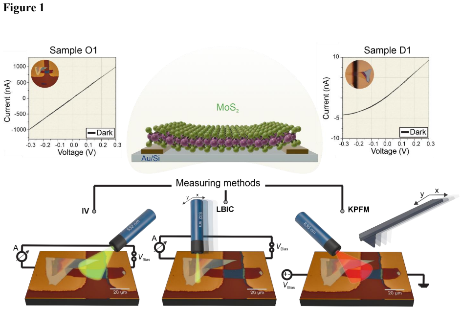
Summary. The manuscript presents a correlative characterization framework for metal contacts to few-layer MoS2 combining (i) dark and illuminated IV, (ii) laser beam induced current (LBIC) mapping at zero and finite bias, and (iii) sideband KPFM operated under a static applied bias (with the zero-bias CPD subtracted), all under ambient conditions and without a gate. Three devices are studied: a 5L flake with ohmic-like behavior (O1) and two 2L diode-like devices (D1, and D2 before/after vacuum annealing). From mutually consistent IV asymmetry, LBIC spatial patterns (photothermoelectric on-contact vs. photovoltaic in-gap), and polarity-dependent KPFM voltage drops, the authors assign barrier types at each contact (Schottky vs. tunnel), decompose the two-terminal resistance via a three-element series model R_total = R_lc + R_sh + R_rc with fractional drops alpha read from KPFM (Table 1), and conclude that annealing lowers total resistance while contact barriers remain dominant. The abstract and conclusion claim the combined analysis "unambiguously" identifies whether the dominant barrier is Schottky or tunnel type.
Significance. If the claims are appropriately calibrated, this is a useful methodological contribution. The combination of bias-dependent KPFM with LBIC and IV on the same device, entirely under ambient conditions and without gating, is a practical, transferable diagnostic that much of the 2D-contacts community could adopt; the annealing case study (D2) demonstrates its relevance to contact optimization. The three measurements are internally consistent across all devices, the KPFM bias-subtraction protocol (forward line biased, backward line at 0 V) is sound, and the series-circuit decomposition is a standard, transparently stated model with order-of-magnitude caveats acknowledged. The paper does not ship ground-truth validation of its barrier-typing rule, however, and its strongest worded claim ("unambiguously") exceeds what the data support — the authors themselves concede the qualitative nature of the identification in §3.4 and point to temperature-dependent IV as the quantitative route. Published with the claims aligned to the evidence, this would be a solid, citable methods paper.
major comments (4)
- [Abstract; §3.4; Conclusion] The claim that the combined analysis 'unambiguously' identifies the barrier type is not supported at the level stated, and is in tension with the manuscript's own text. §3.2 concedes LBIC alone 'cannot unequivocally distinguish' the barrier types; §3.4 retreats to 'a qualitative identification of the barrier types'; and §3.4 itself proposes temperature-dependent IV thermal-activation analysis (ref. 20) as the route to quantitative barrier heights — i.e., the orthogonal ground truth exists and was not performed. The entire typing claim rests on one polarity-dependence decision per diode device (D1: left = Schottky, right = tunnel), with D2's interpretation reusing the same rule without independent validation. Either the abstract/conclusion must be brought in line with §3.4 (qualitative, consistent-with identification), or a validation must be added — e.g., temperature-dependent IV on D1,
- [§3.3 and Table 1 (typing rule)] The core classifier — abrupt polarity-dependent KPFM drop at a contact edge = Schottky; polarity-independent drop = tunnel (vdW gap) — is a model-dependent fingerprint whose uniqueness is not established. A polarity-independent drop is equally consistent with a symmetric pinned junction, sheet/contact-underlay resistance (the authors themselves note the Cr underlayer extends the effective contact in KPFM), or adsorbate/trap-induced series resistance. Under ambient sideband KPFM with a ~25 nm apex, the 0 V-subtraction removes static work-function contrast but not bias- or illumination-dependent artifacts such as photogating (which the authors invoke, ref. 42) or water-layer screening. As a correctness-risk test rather than a circularity objection: the manuscript should (i) explicitly enumerate the alternative origins of a polarity-independent drop and state which observations exclude them
- [§4 (D2 annealing)] The conclusion that annealing reduces a right-contact tunnel barrier and thereby enables a full-width Schottky junction rests on the LBIC signal shift alone; KPFM is shown only after annealing (Fig. 5), so no before/after KPFM comparison supports the claimed redistribution of the voltage drops. Moreover, SI Fig. 14 shows D2's potential profile is laterally inhomogeneous (a triangular region with a shifted drop position, itself interpreted as an additional '(tunnel) barrier'), which complicates the use of single profile lines as representative — the Fig. 3 caption's statement that 'the profile line position is representative of all y-positions' is not demonstrated for D2 and should be qualified. Finally, the KPFM illumination power differs between datasets (5 mW in Fig. 3 vs. 1 mW in Fig. 5), limiting dark/bright comparability across devices.
- [Table 1] The quantitative decomposition has internal inconsistencies. For D1, dark, −0.5 V, the alpha values (72/14/14) sum to 100% in the displayed rounding but the R_prop column (80.00/15.56/15.56) sums to 111.12 MOmega only if alpha values are 72/14/14 — however the +0.5 V dark column gives 38/8/54 (=100%) yet R_prop 12.58/2.65/17.88 sums to 33.11, consistent; please check the −0.5 V bright column (84/8/8 → 1.41/0.13/0.13 sums to 1.67, consistent) and verify all rows, since some rows appear to mix rounded and unrounded alpha. Separately, the 'Barrier Type' column labels O1's left/right contacts 'Schottky / Tunnel' while the text concludes O1 has negligible, ohmic contacts — the label should distinguish 'resistive contact (no rectifying barrier)' from the barrier types, otherwise the table contradicts the paper's own classification of O1.
minor comments (6)
- [Supplementary Material, table of contents and §3.2 caption] The SI table of contents contains unresolved Word cross-reference errors ('Fehler! Textmarke nicht definiert.') for sections 2.5, 3.4, 4.4, and 4.5, and SI Fig. 7's caption refers to 'sample A1' instead of D1. These should be corrected before publication.
- [§2 (illumination conditions)] The power density for global IV illumination is only an estimate ('assuming a laser spot size of roughly 50 um'), and LBIC, global IV, and KPFM use different photon energies and power densities (2.33 eV/100 uW; 2.33 eV defocused; 1.95 eV/1-5 mW). Since Table 1 combines KPFM-derived alpha with IV-derived R_total, a short table summarizing excitation conditions per technique and per figure would help readers assess the stated 'order-of-magnitude' caveat.
- [SI §1.1] Device D1 is fabricated on glass while O1 and D2 are on Si/SiO2, and O1/D1 contacts use shadow masks vs. lithography for D2. Since substrate and contact geometry can affect pinning and thermal coupling (relevant to the PTE assignments), a sentence noting whether any systematic differences were observed or controlled for would be useful.
- [§3.4 (notation)] The fractional-drop parameter alpha is used in Table 1 before its definition appears in the text of §3.4; define it at first use and state explicitly how the contact-edge drop is delimited (spatial window) when reading alpha from the KPFM profiles, given the ~25 nm tip convolution and the Cr-underlayer feature.
- [§4 and Conclusion] The phrase 'ohmic-like Schottky-contact' for D2's right contact after annealing is confusing — a contact is either rectifying (Schottky) or ohmic-like in its IV; please rephrase (presumably: a Schottky junction whose effective resistance after annealing is low enough that the device appears more symmetric).
- [References] Ref. 37 is a trade-magazine web article; a peer-reviewed source for the contact-resistance bottleneck claim would be preferable. Also check ref. 12 page range ('23209–2322') for a typographical truncation.
Circularity Check
No load-bearing circularity: barrier-type assignments are interpretive mappings from standard semiconductor signatures onto new multi-modal data, not identities forced by definition or self-citation.
-
self citation load bearing
[§1 Introduction; §2 Methods; Ref. 38 (Eftekhari et al.)]
"The key methodological advance over prior work lies in the use of KPFM under illumination and an applied static bias voltage38, rather than in the conventional zero-bias work-function mapping mode... Under an applied static bias voltage, KPFM directly maps the spatially resolved voltage drop across the device and thereby quantifies the relative sizes of individual contact barriers without assumptions about the band structure."
The bias-dependent KPFM protocol is justified by a citation whose author list overlaps the present paper (Eftekhari, Saive). This is ordinary methodological self-citation and does not force the Schottky-vs-tunnel conclusion; the barrier-type labels still rest on external junction physics plus the new multi-modal data. Not load-bearing for the central claim—hence only a minor flag.
full rationale
The paper’s central claim—that combined IV, LBIC, and bias-dependent KPFM can identify Schottky vs. tunnel contact barriers and their asymmetry—is an experimental interpretation, not a derivation that reduces to its inputs by construction. IV supplies macroscopic R(V) and illumination dependence; LBIC locates photovoltaic (SCR) vs. photothermoelectric photocurrent; bias-KPFM maps fractional voltage drops α at each contact. The typing rule (polarity-dependent edge drop + gap-centered PV LBIC → Schottky; polarity-independent drop without PV lobe → tunnel) is imported from established junction physics (e.g. Tung Appl. Phys. Rev. 2014; prior photocurrent literature), not defined from the present data and then re-derived. The series decomposition R_total = R_lc + R_sh + R_rc with R_prop = α × R_total (Table 1) is a standard circuit model applied after the fact; the authors explicitly label the numbers order-of-magnitude estimates under mismatched illumination/bias conditions, not independent predictions. Self-citations (Eftekhari et al. MRS Commun. 2026 for the bias-KPFM protocol; Parzinger/Wurstbauer NPJ 2D 2017 for photocurrent morphology) supply methodological precedent and do not force the Schottky/tunnel labels. No uniqueness theorem, fitted-then-predicted quantity, or renamed empirical law appears. Weaknesses (single-device calibration of the typing rule, ambient KPFM confounds, absence of temperature-dependent barrier-height ground truth) are validation/correctness issues, not circularity. Score 1 only for ordinary methodological self-citation that is not load-bearing.
Assumptions & free parameters
free parameters (3)
- Fractional voltage drops α at left contact, channel, right contact =
Device-dependent, e.g. D1 dark +0.5 V: ~38% / ~8% / ~54%
- R_total at KPFM bias from IV =
O1 ~0.3 MΩ; D1 dark ~33–111 MΩ; illuminated lower
- Assumed laser spot size / power density for global IV illumination =
~50 µm diameter (assumed)
assumptions (5)
- domain assumption Photocurrent localized on metal under the flake at zero bias indicates photothermoelectric (Seebeck) response; photocurrent in the gap near a contact indicates photovoltaic response from a space-charge region.
- domain assumption Polarity-dependent abrupt potential drop at a contact in bias-KPFM signals a Schottky barrier; polarity-independent drop signals a tunnel barrier (e.g. vdW gap).
- domain assumption Two-terminal device is well modeled as three series resistors R_lc + R_sh + R_rc whose voltage fractions equal resistance fractions under static bias.
- ad hoc to paper Ambient adsorbates, water, and tip convolution do not invert the Schottky-vs-tunnel spatial/polarity signatures used for identification.
- domain assumption Five-layer MoS2 is near-optimal for low contact resistance relative to bilayer, motivating the O1 vs D1/D2 comparison.
Cite this review
Pith. "Pith review of Identifying Contact Barrier Types in Few-Layer MoS2 Devices Using Correlative IV, LBIC, and Bias-Dependent KPFM." pith.science (2026). https://pith.science/paper/M56KU4KS
@misc{pith2026260725102,
  author       = {Pith},
  title        = {Pith review of: Identifying Contact Barrier Types in Few-Layer MoS2 Devices Using Correlative IV, LBIC, and Bias-Dependent KPFM},
  year         = {2026},
  howpublished = {\url{https://pith.science/paper/M56KU4KS}},
  note         = {Machine review of arXiv:2607.25102}
}
read the original abstract
Electrical contacts between metals and two-dimensional (2D) semiconductors such as molybdenum disulfide (MoS2) critically govern device performance, yet their microscopic nature remains difficult to disentangle using any single characterization technique. Here we present an integrated experimental framework that combines current-voltage (IV) characterization, laser beam induced current (LBIC) mapping, and bias-dependent Kelvin probe force microscopy (KPFM) to comprehensively resolve the contact properties of few-layer MoS2-based two-terminal devices under ambient conditions. IV measurements deliver macroscopic transport characteristics as a function of bias voltage and illumination conditions. LBIC maps the local photocurrent response with micrometer spatial resolution, revealing the position and nature of internal electric fields at MoS2-metal interfaces. KPFM, operated under an applied static bias rather than in the conventional work-function mode, provides nanoscale-resolved potential distributions that quantify the relative magnitudes and spatial locations of contact barriers. We apply this framework to three representative devices - one exhibiting ohmic-like and two exhibiting diode-like contact behavior - and demonstrate that the combined analysis can unambiguously identify whether the dominant barrier is of Schottky or tunnel type and determine the asymmetry between the two contacts. We further demonstrate that thermal annealing significantly reduces the total resistance, while contact barriers remain the dominant source of resistance. The methodology is directly transferable to other 2D semiconductor-metal systems and provides a practical yet comprehensive route toward a quantitative microscopic understanding of 2D device contacts.
Figures


Figures from the paper (2 more)


Reference graph
Works this paper leans on
-
[1]
2 1.1 Optical micrographs
Overview of samples ............................................................................................................... 2 1.1 Optical micrographs ............................................................................................................... 2
-
[2]
3 2.1 IV curves of Sample O1
Overview results IV measurements (dark and illuminated) ......................................................... 3 2.1 IV curves of Sample O1 ........................................................................................................... 3 2.2 IV curves of Sample D1 ................................................................................
-
[3]
6 3.1 Photocurrent data of sample O1 and schemata or according bands
Localized laser beam induced current (LBIC) measurements ..................................................... 6 3.1 Photocurrent data of sample O1 and schemata or according bands .......................................... 6 3.2 Photocurrent data of sample D1 .............................................................................................. 7 ...
-
[4]
11 4.1 KPFM potential data of Sample O1
KPFM measurements with applied voltage .............................................................................. 11 4.1 KPFM potential data of Sample O1 ......................................................................................... 11 4.2 KPFM potential data of Sample D1 ........................................................................
-
[5]
16 5.1 Experimental Setup of electric transport measurements
Measurement methods .......................................................................................................... 16 5.1 Experimental Setup of electric transport measurements ......................................................... 16 5.2 Experimental Setup of Kelvin Probe Force Microscopy .......................................................
-
[8]
In each image the gold contacts are shown with the gap in between
Overview of samples 1.1 Optical micrographs (a) Sample O1 (b) Sample D1 (c) Sample D2 Figure 1 Optical microscope image of the samples O1 in (a), D1 in (b) and D2 in (c). In each image the gold contacts are shown with the gap in between. On top of the contacts and the gap the individual MoS2 flakes of the samples are located. The MoS 2 flakes were fabrica...
-
[9]
The sample is globally excited by laser light with a wavelength of 532 nm and thus with an energy of E𝑙𝑎𝑠𝑒𝑟 = 2.33 eV that is well above the band gap of MoS2
Overview results IV measurements (dark and illuminated) 2.1 IV curves of Sample O1 Figure 2 IV characteristics of sample O1 (left) without light exposure and (right) without light exposure in comparison with the measurements with light exposure at different laser powers of 20, 40, 60, 80 and 100 μW. The sample is globally excited by laser light with a wav...
-
[10]
The laser light with a wavelength of 532 nm is focused on the sample and scanned over it in steps of 2 μm
Localized laser beam induced current (LBIC) measurements 3.1 Photocurrent data of sample O1 and schemata of according bands (a) 0 V (b) 0 V (c) 0.1 V (d) 0.1 V (e) -0.1 V (f) -0.1 V Figure 6 Photocurrent results of sample O1. The laser light with a wavelength of 532 nm is focused on the sample and scanned over it in steps of 2 μm. The photocurrent maps ar...
Show all 12 references
-
[11]
KPFM measurements with applied voltage 4.1 KPFM potential data of Sample O1 Figure 10 The results of the KPFM measurements (in sideband mode under ambient conditions ) are presented for sample O1. (a), (b) and (c) show the results of the measurements at a positive bias voltage...
-
[12]
A voltage is applied to the sample and the current is measured
Measurement methods 5.1 Experimental Setup of electric transport measurements Figure 15 Sketch of the setup of the IV and the local beam induced current (LBIC) measurements. A voltage is applied to the sample and the current is measured. The sample is excited by focused laser ...
-
[363]
(10)Li, S.-L
DOI: 10.1021/nl303321g. (10)Li, S.-L. et al. Thickness Scaling Effect on Interfacial Barrier and Electrical Contact to Two -Dimensional MoS₂ Layers. ACS Nano 2014, 8, 12836–12842. DOI: 10.1021/nn506138y. (11)Kim, C. et al. Fermi Level Pinning at Electrical Metal Contacts of Mo...
2014
-
[3205]
(40)Sadewasser, S
DOI: 10.1021/acsmaterialslett.5c01010. (40)Sadewasser, S. et al. Lateral resolution and potential sensitivity in Kelvin probe force microscopy. Phys. Rev. B 2008, 77, 235427. DOI: 10.1103/PhysRevB.77.235427. (41)Zerweck, U.; Loppacher, Ch.; Otto, T.; Grafström, S.; Eng, L. M. ...
2008 doi
Reviewed July 31, 2026 · model on record in the stance chip above.
Discussion (0). Continue with ORCID to comment.